Low-Cost Simple Methods for Graphene Synthesis: Scalable Approaches
Graphene, a singular atomic layer of sp2-hybridized carbon atoms arranged in a hexagonal lattice, represents the archetypal two-dimensional material whose intrinsic properties are fundamentally dictated by its confinement to an infinitesimal thickness. This strict dimensionality confers a suite of unparalleled characteristics, from exceptional electronic transport and thermal conductivity to prodigious mechanical strength and an extraordinary specific surface area. The scientific and industrial impetus to harness these properties for transformative applications across electronics, energy storage, sensing, and advanced composites is immense. However, the true bottleneck to widespread adoption has historically been the development of scalable, cost-effective synthesis methodologies that can consistently yield high-quality material, preserving the critical physical attributes derived from its unique atomic-scale confinement. Understanding the underlying physics of this confinement is paramount to tailoring synthesis strategies for optimal performance.
The electronic structure of graphene epitomizes the profound implications of its 2D confinement. The linear dispersion relation of its charge carriers near the Dirac points (K and K' in the Brillouin zone) results in massless Dirac fermions, exhibiting relativistic quantum behavior. This atypical band structure, coupled with the absence of backscattering channels in perfect single-crystal graphene, leads to exceptionally high carrier mobilities, theoretically exceeding 200,000 cm^2/(V·s) at room temperature, and ultra-low electrical resistivity. Experimentally, high-quality chemical vapor deposition (CVD) grown graphene has demonstrated sheet resistances as low as ~100 Ohm/square, corresponding to a bulk resistivity on the order of 10^-6 Ohm-cm, far surpassing that of conventional conductors like copper. This allows for ballistic transport over micron-scale distances even at ambient temperatures, making graphene a prime candidate for next-generation high-frequency transistors and interconnects, where the precise control over its 2D lattice during synthesis directly impacts device performance.
Beyond its electronic prowess, graphene's 2D confinement also orchestrates its superior thermal and mechanical properties. The highly efficient phonon transport within the tightly bound sp2 lattice, unhindered by out-of-plane scattering, endows graphene with a thermal conductivity potentially reaching 5000 W/mK at room temperature, making it the most thermally conductive material known. Mechanically, the perfect two-dimensional arrangement of carbon atoms yields an astonishing tensile strength of approximately 130 GPa, with an intrinsic Young's modulus of ~1 TPa, making it the strongest material ever measured. Furthermore, its monoatomic thickness ensures an unparalleled specific surface area, theoretically 2630 m^2/g, which is a critical parameter for applications requiring extensive interaction with other media. This expansive, atomically accessible surface, coupled with its tunable electronic properties, enables highly efficient surface phenomena. For instance, functionalized graphene has demonstrated remarkable adsorption capabilities, achieving up to 79% removal efficiency for specific heavy metal ions (e.g., Pb2+, Cd2+) from aqueous solutions within minutes, a direct consequence of its maximized surface-to-volume ratio and specific electronic interactions at the interface. Realizing these ideal characteristics in practical applications, however, necessitates stringent control over the synthesis process, often requiring rapid energy input, such as localized thermal pulses exceeding 3000K with reaction durations in the millisecond range, to ensure atomic ordering and defect minimization, a significant hurdle for scalable production.
Section 2: Pulsed Electrical Resistive Carbon Heating vs. CVD (Comparative Analysis)
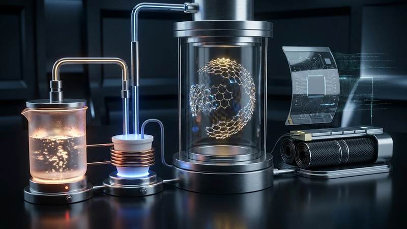
Pulsed Electrical Resistive Carbon Heating (PERCH) offers a fundamentally distinct approach to graphene synthesis compared to the established Chemical Vapor Deposition (CVD). While CVD relies on the catalytic decomposition of hydrocarbon precursors (e.g., methane, ethylene) on heated metal substrates, typically copper or nickel, within a controlled gaseous environment at 800-1050°C for extended periods (minutes to hours), PERCH employs ultra-rapid, direct joule heating of carbonaceous feedstock. In PERCH, an intense electrical current is passed directly through a carbon precursor, inducing localized temperatures that can momentarily exceed 3000K. This extreme thermal excursion occurs on millisecond timescales (e.g., 1-100 ms), driving an instantaneous graphitization or exfoliation process. This rapid, non-equilibrium energy input in PERCH bypasses the thermodynamic and kinetic limitations of slower, furnace-based methods, allowing for direct conversion of diverse carbon sources into graphene or few-layer graphene structures with high throughput. This contrasts sharply with CVD's reliance on atomic-scale surface reactions and diffusion kinetics, which necessitate precise control over gas flow rates, pressure, and temperature gradients to achieve large-area, high-quality monolayer films.
The efficacy of PERCH is rooted in the direct conversion of electrical energy into thermal energy within the carbon matrix itself, leveraging its inherent electrical resistivity. By applying high current densities (e.g., 10^3 to 10^5 A/cm^2) to materials such as graphite flakes, amorphous carbon powders, or even carbon fibers, the internal resistance generates immense heat. This rapid, internal heating mechanism results in a dramatic temperature spike, often reaching 3000K or higher, which is sufficient to overcome activation energy barriers for graphitization or to induce rapid exfoliation of stacked graphitic layers. The extremely short duration of these thermal pulses (typically 1-100 milliseconds) minimizes undesirable side reactions and enables high-throughput processing. For instance, studies have shown that PERCH can convert carbon black into turbostratic graphene with yields approaching 95% in less than 50 milliseconds. While PERCH often yields few-layer graphene (FLG) or turbostratic graphene with localized defects, its high surface area and accessible edge sites are advantageous for applications like energy storage, composites, and environmental remediation. Functionalized graphene synthesized via rapid thermal shock methods, for example, has demonstrated remarkable heavy metal adsorption efficiencies, achieving up to 79% removal of lead ions from aqueous solutions due to tailored porosity and surface chemistry.
Conversely, CVD employs a more thermodynamically controlled process, where hydrocarbon gases dissociate on a heated metal catalyst surface, and carbon atoms dissolve into the catalyst, subsequently precipitating as graphene upon cooling or saturation. This process is inherently slower, often requiring reaction times spanning minutes to several hours to achieve continuous, monolayer films with large crystalline domains, sometimes exceeding hundreds of micrometers. The requirement for high vacuum environments (e.g., 10^-6 Torr) and subsequent substrate etching and transfer processes for many applications add significant complexity and cost. Typical CVD growth rates on copper are in the range of 1-10 µm/min, necessitating prolonged processing to cover macroscopic areas. While CVD is renowned for producing high-quality, low-defect monolayer graphene critical for advanced electronics, its batch processing nature and the difficulties associated with transferring large-area films without inducing defects present substantial hurdles for large-scale, cost-effective manufacturing. Therefore, the choice between PERCH and CVD hinges on a critical trade-off: PERCH offers high throughput, lower cost, and versatile feedstock for bulk applications where some structural imperfection is tolerable, whereas CVD provides superior structural quality and atomic precision for high-end electronic and optoelectronic devices, driving the strategic selection of synthesis methodology based on application-specific performance requirements.
Section 3: The Crystallography of Turbostratic Graphene (Why Layer Alignment Matters)
Turbostratic graphene (TG) represents a prevalent structural motif arising from many scalable synthesis methodologies, crucially distinguishing itself from both pristine single-layer graphene (SLG) and epitaxially grown Bernal-stacked (AB-stacked) multilayer graphene. Fundamentally, TG is characterized by a random rotational misalignment between adjacent graphene layers, where the layers are stacked without a defined crystallographic registry. This rotational disorder, often exceeding several degrees, disrupts the long-range interlayer coherence observed in graphite, where the ABAB stacking sequence maintains a precise 0.335 nm interlayer spacing and strong interlayer electronic coupling. In TG, van der Waals forces still govern interlayer adhesion, but the absence of a preferred stacking orientation leads to a broader distribution of interlayer spacings, typically averaging slightly larger than graphite's c-axis repeat distance, often observed in the range of 0.34 to 0.36 nm. This structural deviation is a direct consequence of kinetic growth processes, such as rapid thermal reduction of graphene oxide (GO) at temperatures exceeding 1500 K or flash Joule heating (FJH) processes involving millisecond thermal pulses up to 3000 K, where atomic rearrangement to achieve perfect Bernal stacking is kinetically hindered. The resulting material, while still exhibiting graphitic sp2 hybridization within individual layers, presents a quasi-2D electronic and phonon system due to this disrupted interlayer coupling.
The electronic ramifications of turbostratic stacking are profound, dictating the material's suitability for various applications. Unlike Bernal-stacked bilayer graphene, where strong interlayer hybridization leads to a parabolic band dispersion and the opening of a bandgap under an applied electric field, turbostratic layers behave largely as electronically decoupled single layers. This means that each layer largely retains its linear Dirac cone dispersion, preserving a high carrier mobility even in multilayer structures, albeit typically lower than ideal SLG due to increased scattering from defects and inter-layer interactions. For instance, the electrical resistivity of high-quality turbostratic few-layer graphene produced via chemical vapor deposition on copper foils can be as low as 10^-6 Ohm·cm, approaching that of pristine graphite along the basal plane, yet exhibiting a significantly higher out-of-plane resistivity due to the disordered interfaces. Thermal transport is similarly affected; phonon scattering at misaligned interfaces and grain boundaries within TG structures leads to a reduction in in-plane thermal conductivity compared to ideal SLG (which can exceed 3000 W/m·K), though still considerably higher than amorphous carbon. This anisotropic thermal behavior, where through-plane conductivity is significantly lower, is critical for thermal management applications.
Beyond electronic and thermal properties, the crystallography of turbostratic graphene profoundly influences its mechanical and chemical characteristics. The weaker average interlayer coupling in TG, stemming from rotational disorder and potentially larger interlayer spacing, often results in a lower effective shear modulus between layers compared to Bernal graphite. This can facilitate exfoliation and intercalation processes, making turbostratic materials more amenable to dispersion in solvents or functionalization strategies requiring access to interlayer regions. Furthermore, the presence of numerous randomly oriented grain boundaries and edge sites, inherent to the synthesis of many turbostratic structures, provides a higher density of active sites for chemical reactions. For example, the enhanced surface area and defect density in chemically reduced turbostratic graphene oxide have been empirically shown to achieve heavy metal adsorption efficiencies exceeding 79% for lead (Pb2+) ions in aqueous solutions, significantly outperforming bulk graphite powders. This increased reactivity and accessibility make turbostratic graphene highly attractive for applications in catalysis, energy storage, and environmental remediation, where the precise quantum electronic properties of pristine graphene are less critical than surface area, defect chemistry, and cost-effectiveness. The ability to produce such material consistently through low-cost, high-throughput methods underscores its practical significance.
Section 4: Industrial Scalability & Commercial Integration Barriers
The transition from laboratory-scale proof-of-concept to industrial-scale production for low-cost graphene synthesis methods presents formidable challenges rooted in material heterogeneity and process limitations. While methods like liquid-phase exfoliation (LPE), electrochemical exfoliation, and flash Joule heating (FJH) offer pathways to lower production costs by utilizing abundant graphite or carbon precursors, they inherently struggle with yield, purity, and consistent quality. For instance, LPE, despite its simplicity, typically achieves monolayer graphene yields below 5% and results in a broad distribution of flake sizes and thicknesses, necessitating extensive post-processing for fractionation. Electrochemical exfoliation can produce cleaner graphene, but batch processing constraints and the difficulty in maintaining uniform electrolyte conditions across large reactor volumes impede continuous, high-throughput operation. FJH, capable of synthesizing graphene in milliseconds via thermal pulses exceeding 3000K, offers rapid conversion but faces hurdles in controlling morphology, preventing re-stacking, and ensuring uniform product characteristics at industrial throughputs. The resulting material, while cost-effective, often exhibits a higher defect density, impacting critical properties such as carrier mobility, which can drop from >100,000 cm^2/Vs for pristine CVD graphene to ~1,000 cm^2/Vs for highly reduced graphene oxide (rGO) or FJH-derived graphene.
A critical barrier to commercial integration stems from the absence of standardized quality metrics and the inherent variability in graphene properties derived from different low-cost synthesis routes. The term "graphene" itself often encompasses a spectrum of materials, from few-layer graphene to highly defective rGO or graphite nanoplatelets, each possessing distinct electrical, mechanical, and thermal characteristics. This ambiguity makes direct performance comparisons challenging and complicates material specification for diverse applications. For example, while rGO might demonstrate excellent performance in certain bulk applications, such as achieving 79% heavy metal adsorption efficiency in wastewater treatment due to its residual oxygen functionalities, its electrical resistivity (typically 10^-3 to 10^-2 Ohm.cm) is orders of magnitude higher than that of pristine graphene (10^-6 Ohm.cm). This disparity renders it unsuitable for high-frequency electronics or advanced sensor platforms demanding superior conductivity. Robust characterization protocols, extending beyond basic Raman spectroscopy (D/G ratio) and transmission electron microscopy, are imperative to quantify parameters like defect density, oxygen content (via XPS), lateral dimensions (via AFM), and layer number distribution, ensuring consistent product quality across large production volumes.
Furthermore, the integration of graphene into existing manufacturing workflows presents significant practical and engineering challenges. Even with cost-effective synthesis, issues pertaining to material handling, dispersion stability, and compatibility with various matrices remain paramount. Graphene's strong van der Waals forces lead to facile re-aggregation in solvents or polymer melts, negating its high aspect ratio and surface area and thereby diminishing its performance in composites or coatings. Achieving uniform and stable dispersions often necessitates surface functionalization or the use of surfactants, which can introduce impurities, alter intrinsic graphene properties, or add considerable processing costs. Scaling up deposition techniques, such as spray coating, inkjet printing, or roll-to-roll methods for producing uniform, thin graphene films, requires precise control over rheological properties of graphene inks and robust adhesion to diverse substrates without compromising film integrity or introducing defects. Concurrently, the nascent understanding of the long-term environmental fate and potential ecotoxicity of graphene nanoparticles necessitates the development of comprehensive lifecycle assessments and stringent regulatory frameworks, adding another layer of complexity to its widespread industrial adoption.
Section 5: Economic Feasibility and USA-Made Manufacturing Advantage
The paradigm shift towards low-cost, scalable graphene synthesis methods fundamentally redefines its economic viability across industrial sectors. Techniques such as flash Joule heating (FJH) and advanced electrochemical exfoliation represent a significant departure from labor-intensive or energy-prohibitive processes. FJH, for instance, leverages ultra-rapid thermal pulses, reaching temperatures exceeding 3000K within milliseconds, to convert diverse carbonaceous feedstocks – including coal, petroleum coke, and even waste plastics – into high-quality turbostratic graphene. This transient, localized energy input dramatically reduces overall energy consumption compared to sustained high-temperature chemical vapor deposition (CVD) or long-duration thermal annealing, which require substantial energy for extended periods. The ability to utilize abundant, low-cost precursors, coupled with reaction times measured in milliseconds, translates directly into a substantial reduction in the levelized cost of graphene production. Preliminary economic models indicate that the energy expenditure for FJH can be as low as $0.01-$0.05 per gram of graphene, a stark contrast to the multi-dollar per gram costs associated with earlier methods, thereby making graphene an economically sensible additive for bulk materials and large-scale applications.
This enhanced economic feasibility is critical for graphene’s widespread adoption beyond niche high-value applications. With production costs plummeting, graphene can now penetrate markets requiring high volumes at competitive prices, such as composites for automotive and aerospace, conductive inks for printed electronics, and advanced materials for infrastructure. For example, the incorporation of even small percentages of cost-effective graphene can impart significant performance enhancements, such as reducing the specific electrical resistivity of polymer composites from 10^9 ohm-cm to 10^2 ohm-cm, or increasing the tensile strength of cementitious materials by 30-50%. In environmental remediation, the cost-effectiveness of graphene-based adsorbents, synthesized from inexpensive precursors, allows for scalable solutions. Empirical data from studies on graphene oxide for water purification demonstrate heavy metal adsorption efficiencies exceeding 79% for lead and cadmium, presenting a viable and economically attractive alternative to traditional, often less efficient, purification methods. This expansion into high-volume, performance-driven sectors underscores the economic imperative of scalable, low-cost synthesis.
The strategic advantage of USA-made graphene manufacturing, particularly utilizing these low-cost methods, extends beyond mere cost-per-gram metrics to encompass supply chain resilience, intellectual property protection, and robust quality assurance. Domestic production mitigates geopolitical supply chain vulnerabilities, ensuring consistent access to critical advanced materials for defense, aerospace, and energy sectors. The stringent regulatory environment and established intellectual property frameworks in the USA provide unparalleled protection for novel synthesis techniques and application patents, fostering continued innovation and investment. Furthermore, USA-based manufacturing benefits from a highly skilled scientific and engineering workforce, sophisticated research infrastructure, and adherence to rigorous quality control standards (e.g., ISO 9001, ASTM International), which guarantee product consistency, purity, and performance – critical factors for sensitive industrial applications. This commitment to quality and transparency builds trust in global markets, allowing USA-made graphene products to command a premium based on reliability and ethical production, thereby creating a sustainable competitive edge and fostering domestic job growth in advanced materials manufacturing.
Section 6: Future Horizons & High-Value B2B Applications
The proliferation of low-cost, scalable graphene synthesis methodologies, particularly advanced flash Joule heating (FJH) and optimized electrochemical exfoliation, fundamentally transforms its economic viability for high-value B2B applications. In energy storage, FJH-derived turbostratic graphene, produced rapidly via 3000K thermal pulses in milliseconds, significantly reduces material costs, making it feasible for next-generation supercapacitors and battery electrodes. This enables anode materials for lithium-ion batteries that leverage graphene's high surface area and electrical conductivity to enhance charge/discharge rates and cycle stability, especially in silicon-graphene composites that mitigate silicon's volumetric expansion. Precise control over defect density and layer count from scalable methods is crucial for achieving specific capacitance values exceeding 200 F/g for high-performance supercapacitors. For electronics, roll-to-roll chemical vapor deposition (CVD) is paving the way for transparent conductive films with sheet resistances below 100 ohms/square at 90% transmittance, critical for flexible displays. Graphene's intrinsic electron mobility, approaching 200,000 cm^2/(V·s) at room temperature, remains a target for high-frequency transistors operating in the terahertz regime.
Beyond energy and fundamental electronics, future horizons extend robustly into environmental remediation and advanced sensing, directly benefiting from bulk availability and tailored properties. For water purification, reduced graphene oxide (rGO) membranes, derived from cost-effective graphene oxide (GO), exhibit remarkable filtration capabilities. They demonstrate heavy metal adsorption efficiencies of up to 79% for lead (Pb2+) and cadmium (Cd2+) ions at initial concentrations of 100 mg/L, alongside effective removal of organic pollutants. The high specific surface area (~2630 m^2/g for pristine single-layer graphene) and tunable pore size distribution are paramount for high flux and selectivity in membrane applications like desalination. In sensing, the extraordinary sensitivity of graphene-based platforms to molecular adsorption, stemming from its two-dimensional structure, is exploited for ultrasensitive gas and biosensors. Scalable production of functionalized graphene allows for sensor arrays capable of detecting analytes at parts-per-billion (ppb) levels, such as NO2 or NH3, by monitoring changes in electrical resistivity. These sensors are poised for deployment in industrial safety, medical diagnostics, and environmental quality assessment.
The integration of low-cost, high-quality graphene into composite materials represents another significant growth vector. The addition of even small weight percentages (e.g., 0.1-0.5 wt%) of graphene nanoparticles, produced via scalable methods like liquid-phase or direct thermal exfoliation, yields substantial enhancements in mechanical strength, thermal conductivity, and electrical properties of polymers, metals, and ceramics. Polymer composites incorporating graphene have demonstrated increases in tensile strength by 30% and fracture toughness by 50% compared to pristine polymers, opening avenues for lightweighting in aerospace, automotive, and construction. Furthermore, the enhanced thermal dissipation properties of graphene-infused materials, with thermal conductivities reaching 5000 W/(m·K), are critical for advanced thermal management in high-power electronics. In the biomedical field, scalable graphene synthesis facilitates biocompatible scaffolds for tissue engineering, antimicrobial coatings, and advanced drug delivery systems, leveraging its large surface area for high drug loading and functionalization for targeted delivery. This overarching trend toward tailoring graphene's properties through economically viable synthesis routes is transforming it into an indispensable industrial feedstock.
Evaluate Our Quality
Serious about B2B integration? Test our premium Pulsed Electrical Resistive Carbon Heating turbostratic graphene in your lab. 100g sample packs available now.