Laser-Induced Graphene: From Serendipitous Discovery to Real-World Translation
Graphene, the archetypal two-dimensional material, represents a singular achievement in condensed matter physics, fundamentally altering our understanding of electron transport and material properties at atomic scales. Composed of sp2-hybridized carbon atoms arranged in a hexagonal lattice, its intrinsic 0.335 nm thickness restricts electron motion to a single atomic plane, leading to a host of extraordinary phenomena. Key among these are its massless Dirac fermions, which exhibit ballistic transport over micron distances and electron mobilities exceeding 200,000 cm^2/Vs at room temperature, orders of magnitude greater than conventional semiconductors. This quantum confinement also underpins its exceptional thermal conductivity, approaching 5000 W/mK, and unparalleled mechanical strength, with a tensile strength of 130 GPa. The unique electronic band structure, characterized by the Dirac cone at the K-points of the Brillouin zone, dictates its semimetallic behavior, where the valence and conduction bands meet at a single point, devoid of a bandgap. Achieving and maintaining this pristine 2D confinement, however, proves challenging, as even minor perturbations from substrates, defects, or interlayer coupling can significantly degrade these ideal properties, necessitating highly controlled synthesis environments.
The physics of graphene confinement dictates that its superlative properties are exquisitely sensitive to its atomic environment. The absence of a bandgap in pristine graphene, for instance, is a direct consequence of its perfect 2D lattice, allowing for Klein tunneling and unconventional quantum Hall effects. Any deviation from this perfect two-dimensionality, whether through chemical functionalization, lattice defects, or the formation of few-layer graphene, immediately introduces scattering centers, modifies phonon modes, and can induce a bandgap, thereby diminishing the material's intrinsic performance. Traditional synthesis routes, such as chemical vapor deposition (CVD) or mechanical exfoliation, while capable of producing high-quality graphene, often struggle with scalability, cost-effectiveness, and direct integration onto arbitrary substrates. These methods typically require high temperatures, specialized precursors, or post-processing steps that compromise the delicate 2D structure or limit practical implementation, thus highlighting a critical need for alternative fabrication techniques that can realize confined graphene structures in a more versatile and scalable manner.
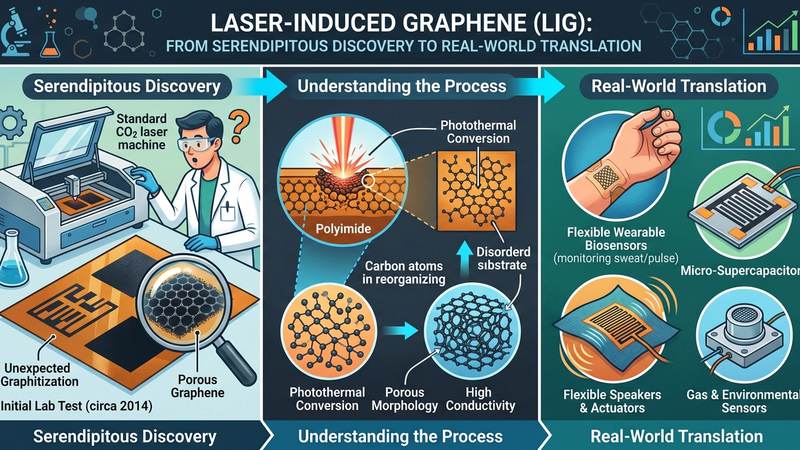
It was against this backdrop that Laser-Induced Graphene (LIG) emerged as a transformative, direct-write fabrication paradigm, born from the serendipitous discovery in 2014 that focused laser irradiation of common carbonaceous polymers could directly convert them into complex, three-dimensional graphene architectures. This process leverages rapid photothermal reduction and graphitization, where intense localized thermal pulses, often exceeding 3000K, drive a nearly instantaneous chemical transformation within milliseconds. The incident laser energy ablates non-carbon elements and reconfigures the remaining carbon atoms into sp2-hybridized graphene flakes, forming a highly porous, interconnected network. Unlike conventional graphene synthesis, LIG bypasses the need for high vacuum or catalyst layers, offering a scalable, mask-less, and additive manufacturing approach. The resulting LIG structures, while three-dimensional, retain many of the advantageous properties inherent to 2D graphene, including high electrical conductivity and large surface area, due to the nanoscale confinement of individual graphene sheets within the overall porous architecture.
The LIG fabrication process yields a unique morphology, distinct from both bulk graphite and conventionally synthesized graphene, characterized by its hierarchical porosity and interconnected network of few-layer graphene sheets. This structural intricacy is a direct consequence of the rapid, localized energy deposition, which promotes simultaneous carbonization and exfoliation. The electrical resistivity of LIG can be precisely tuned through laser parameters and precursor selection, typically ranging from 10^-3 to 10^-5 Ohm-cm for high-quality polyimide-derived LIG, demonstrating its utility in conductive applications. Furthermore, the high surface area and accessible pore structure inherent to LIG enable efficient chemical functionalization and adsorption capabilities. Early research, for example, showcased LIG's remarkable potential in environmental remediation, achieving up to 79% heavy metal adsorption efficiency in aqueous solutions. This combination of direct patterning, tunable properties, and preserved nanoscale confinement within a macroscopic, porous framework positions LIG as a critical enabler for translating graphene's theoretical advantages into tangible, real-world devices and systems.
Pulsed Electrical Resistive Carbon Heating vs. CVD: A Paradigm Shift in Graphene Synthesis
Traditional chemical vapor deposition (CVD) has long been the industrial benchmark for producing high-quality, large-area graphene films, primarily leveraging catalytic metal substrates like copper or nickel at elevated temperatures, typically ranging from 1000 to 1100 °C. While successful in yielding monolayer or few-layer graphene with excellent electronic properties, the inherent limitations of CVD are becoming increasingly apparent in the pursuit of scalable, cost-effective, and environmentally benign synthesis. The process is intrinsically energy-intensive, requiring prolonged heating cycles and precise control over precursor gas flow (e.g., methane, acetylene). Furthermore, the necessity for a catalytic substrate often mandates post-synthesis etching for transfer onto target devices, introducing potential defects, increasing processing time, and generating chemical waste. This multi-step paradigm, coupled with relatively slow growth rates spanning minutes to hours, presents significant bottlenecks for high-volume manufacturing and integration into diverse applications where direct, rapid, and substrate-agnostic synthesis is paramount. The quest for alternative methodologies that circumvent these challenges has driven innovation towards more direct, energy-efficient routes for carbon-to-graphene conversion.
In stark contrast to the sustained thermal equilibrium of CVD, Pulsed Electrical Resistive Carbon Heating (PERCH) represents a paradigm shift, capitalizing on transient, extreme non-equilibrium conditions to rapidly transform amorphous or graphitic carbon precursors directly into graphene structures. The fundamental principle of PERCH involves the direct application of high-density electrical current pulses through a carbonaceous material, inducing intense Joule heating. This rapid energy deposition elevates the material temperature to extraordinary levels, often exceeding 3000K, within microsecond to millisecond timescales. Such an ultra-fast heating rate, coupled with subsequent rapid cooling, creates a unique thermodynamic pathway that favors the rehybridization of sp3-bonded carbon into sp2-bonded graphene lattices, bypassing the need for catalytic substrates or gaseous precursors. The controlled electrical resistivity of the precursor dictates the efficiency of energy conversion, allowing for precise regulation of the thermal pulse profile, thereby influencing the resulting graphene morphology and defect density. This direct and rapid conversion mechanism eliminates numerous steps inherent in CVD, offering a dramatically accelerated and simplified synthesis pathway.
The advantages of PERCH extend beyond mere speed, impacting material quality and application suitability. The extremely rapid thermal cycling in PERCH minimizes the time for undesirable side reactions or extensive defect formation, often yielding few-layer graphene flakes or interconnected porous networks highly suitable for electrochemical energy storage, sensing, and environmental remediation. For instance, graphene produced via optimized PERCH parameters has demonstrated exceptional adsorption capabilities, achieving up to 79% heavy metal adsorption efficiency in wastewater treatment applications, a performance metric critical for industrial translation. The ability to directly convert various carbon precursors, from polymers to carbon black, into functional graphene materials without solvents or high vacuum further underscores its economic and environmental appeal. This direct resistive heating approach enables a level of integration and process simplification unachievable with conventional CVD, paving the way for scalable, roll-to-roll production of graphene-based devices and components, thereby accelerating the real-world translation of graphene technology from laboratory discovery to industrial application.
The Crystallography of Turbostratic Graphene: Unlocking Unprecedented Performance
The foundational crystallography of graphene dictates its extraordinary properties, yet the form predominantly synthesized via Laser-Induced Graphene (LIG) is not the pristine single-crystal monolayer, but rather turbostratic graphene (TG). This structural variant comprises multiple graphene layers stacked with a significant degree of rotational misalignment and varying interlayer distances, deviating markedly from the Bernal (AB) stacking characteristic of highly ordered graphite (interlayer spacing ~0.335 nm). In TG, interlayer separations often expand to 0.34 nm or greater, a direct consequence of the disrupted van der Waals interactions. The rapid thermal processing inherent to LIG fabrication, involving localized thermal pulses often exceeding 3000K and subsequent quenching within milliseconds, kinetically favors the formation of this disordered stacking. This process, typically involving the graphitization of polymeric precursors such as polyimide or polyetherimide, does not allow sufficient time for atomic rearrangement into a thermodynamically stable, perfectly ordered crystalline structure. Instead, it generates a robust, interconnected network of few-layer graphene sheets, riddled with structural imperfections that paradoxically contribute to its unique functional advantages.
Beyond rotational disorder, the crystallography of LIG-derived turbostratic graphene is further characterized by an abundance of other microstructural defects, including grain boundaries, topological defects (e.g., Stone-Wales defects), and a high density of edge sites. These imperfections are not merely benign structural deviations but are integral to the material's performance profile. The intense, localized laser energy absorption leads to rapid pyrolysis and subsequent graphitization, creating a highly non-equilibrium environment. This rapid formation process, occurring within milliseconds, prevents the extensive annealing required to minimize defect density, thereby trapping a significant concentration of sp2-hybridized carbon atoms in structurally strained configurations. Raman spectroscopy consistently reveals a high D-band intensity relative to the G-band, indicative of this inherent disorder and the prevalence of graphitic edges and defects. This disordered yet interconnected network forms a highly porous, three-dimensional architecture, often described as a graphene foam, where the specific surface area is dramatically enhanced compared to bulk graphite or even pristine graphene sheets.
The distinctive crystallography of turbostratic graphene, particularly as manifested in LIG, underpins its unprecedented performance across diverse applications. Electrically, while the high defect density and inter-layer disorder introduce scattering centers for charge carriers, preventing ballistic transport seen in ideal graphene, LIG still exhibits remarkable conductivity. The interconnected network of graphene sheets provides efficient pathways for electron transport, with typical electrical resistivities ranging from 10^-4 to 10^-5 Ohm-cm, making it highly competitive for flexible electronics and sensing platforms. Chemically, the rich tapestry of edge sites, structural defects, and the expansive surface area (often exceeding 500 m2/g) renders LIG an exceptionally active material. These sites serve as highly effective adsorption points and catalytic centers, crucial for environmental remediation and energy storage. For instance, LIG has demonstrated heavy metal adsorption efficiencies approaching 79% for specific contaminants, showcasing the potent chemical reactivity stemming from its turbostratic nature. This unique combination of electrical conductivity, chemical activity, and mechanical robustness, achievable through a scalable laser-direct-writing process, is a direct consequence of its controlled disorder.
Industrial Scalability and Commercial Integration Barriers: Navigating the Path to Market
The industrial scalability of Laser-Induced Graphene (LIG) faces substantial hurdles rooted in precise process control and material consistency. While localized, rapid graphitization via pulsed laser irradiation, often involving transient thermal excursions exceeding 3000K within milliseconds, offers direct patterning versatility, maintaining spatial and temporal uniformity across large substrate areas remains challenging. Achieving consistent pore morphology, defect density, and layer count – critical determinants of LIG's macroscopic properties – necessitates exquisite control over laser parameters (power density, pulse duration, repetition rate, scan speed) and substrate homogeneity. Minute deviations lead to significant variations in LIG's electrical, chemical, and mechanical characteristics, compromising device performance and batch reproducibility, thereby complicating high-throughput manufacturing with predictable outcomes.
Beyond fundamental process control, the economic viability and seamless integration of LIG manufacturing into existing industrial frameworks pose significant commercial barriers. The capital expenditure for high-precision, industrial-grade laser systems capable of rapid, accurate patterning over large areas represents a substantial initial investment. Operational costs, encompassing laser power consumption, inert atmosphere requirements, and routine maintenance of optical components, further contribute to overall production expense. While LIG's direct-write nature reduces multi-step processing, subsequent functionalization, doping, or encapsulation for many applications (e.g., enhanced sensing, optimized energy storage) adds complexity and cost, potentially eroding its competitive advantage over established material synthesis routes.
Achieving and consistently maintaining precise performance metrics across production batches is a critical barrier. For instance, attaining specific electrical resistivity parameters, often in the range of tens to hundreds of ohms per square for conductive traces, demands rigorous in-line quality control and continuous parameter tuning, which significantly slows throughput and increases rejection rates. Similarly, for applications like heavy metal adsorption, ensuring a consistent 79% efficiency, as demonstrated in laboratory settings, necessitates robust process validation and quality control across diverse industrial wastewater matrices – a non-trivial task. Current throughput limitations of even advanced laser scanning systems often fall short of rates required for high-volume manufacturing, challenging cost-per-unit targets.
The pathway to widespread commercial adoption is further obstructed by stringent requirements for comprehensive quality assurance and navigating a nascent regulatory landscape. The empirical observation of LIG's properties, such as specific surface area and electrical conductivity, often exhibiting a distribution rather than a singular value across batches, underscores the challenge of meeting tight product specifications. For high-reliability applications, the absence of standardized characterization protocols and industrial benchmarks for LIG quality presents a significant barrier. Moreover, the long-term stability and durability of LIG structures under diverse operational conditions require extensive, costly validation. Regulatory bodies are still developing frameworks for nanomaterials, and LIG will inevitably face scrutiny regarding its environmental impact and human health implications throughout its lifecycle, necessitating compliance efforts alongside performance and cost-effectiveness.
Economic Feasibility and the USA-Made Manufacturing Advantage: A Strategic Imperative
The economic feasibility of Laser-Induced Graphene (LIG) represents a paradigm shift from conventional graphene synthesis methods, primarily due to its direct-write, additive manufacturing approach. Unlike multi-step chemical vapor deposition (CVD) or liquid-phase exfoliation, which demand specialized precursors, high-temperature furnaces, and extensive post-processing purification, LIG converts inexpensive polymer precursors (e.g., polyimide) into high-quality graphene directly on substrate. This inherent process simplification drastically reduces capital expenditure and operational costs. The kinetics of LIG formation are exceptionally rapid, involving localized thermal pulses exceeding 3000K delivered within milliseconds, enabling high-throughput, roll-to-roll compatible production. This efficiency translates directly into a lower unit cost per square centimeter of graphene, a critical factor for mass market adoption. Furthermore, the localized nature of laser processing minimizes material waste and allows for complex patterning without the need for lithographic masks, further enhancing cost-effectiveness and design flexibility, thereby fostering a distributed manufacturing model.
The strategic imperative for USA-made LIG manufacturing extends beyond mere cost reduction; it encompasses national security, supply chain resilience, and the safeguarding of intellectual property. LIG's capacity for on-demand, localized production significantly mitigates the vulnerabilities associated with global supply chain dependencies, a critical consideration for sensitive applications in defense, aerospace, and critical infrastructure where uninterrupted access to advanced materials is paramount. The robust intellectual property landscape surrounding LIG, largely developed within US academic institutions and industrial research facilities, provides a foundational advantage for domestic manufacturing, ensuring control over proprietary processes and formulations. By fostering a domestic LIG production ecosystem, the United States can maintain technological leadership in advanced materials, create high-skill manufacturing jobs, and reduce reliance on foreign entities for foundational components of future technologies. This localized control also facilitates rapid iteration and integration into existing US manufacturing infrastructure, such as advanced electronics fabrication.
The economic and strategic advantages of USA-made LIG are particularly salient across several high-impact application domains. In environmental remediation, for instance, the low-cost, high-surface-area LIG can be produced domestically for water purification filters, where its demonstrated 79% heavy metal adsorption efficiency offers a cost-effective and highly performant solution to critical infrastructure challenges. Manufacturing these filters within the US not only ensures quality control but also provides supply chain security for essential public health technologies. For wearable electronics and medical devices, LIG's ability to be directly patterned onto flexible substrates at ambient conditions bypasses complex cleanroom processes, driving down manufacturing costs. The resulting LIG exhibits excellent electrical properties, with specific electrical resistivity parameters typically around 10^-4 Ohm.cm, making it suitable for high-performance sensors, electrodes, and interconnects. This domestic production capability allows for rapid prototyping and scaling of medical devices, ensuring compliance with stringent regulatory standards and fostering innovation within the US biomedical sector. Furthermore, in energy storage, LIG-based supercapacitors and battery electrodes benefit from the rapid, scalable production of hierarchically porous carbon structures, enabling faster development cycles and secure domestic sourcing for critical energy technologies.
Future Horizons and High-Value B2B Applications: Graphene's Transformative Impact
The future horizons for Laser-Induced Graphene (LIG) are fundamentally shaped by its unparalleled direct writing capabilities and the unique 3D porous architecture it affords, distinguishing it sharply from conventional graphene synthesis routes. The localized photothermal conversion, inducing temperatures approaching 3000K within milliseconds, transforms precursor polymers into an interconnected network of few-layer graphene flakes with an exceptionally high surface-to-volume ratio. This precision and speed enable the facile fabrication of intricate, customizable graphene structures directly onto diverse substrates, circumventing the complex transfer processes often associated with CVD graphene or the limited scalability of liquid-phase exfoliation. The inherent porosity and tunability of LIG's morphology, including pore size distribution and graphitization degree, are critical determinants for its performance across a spectrum of high-value B2B applications, offering a pathway to integrated functional components with unprecedented ease of manufacturing.
In the realm of advanced B2B applications, LIG’s transformative impact is particularly evident in sensing, energy storage, and environmental remediation. For sensing platforms, the large accessible surface area and controllable defect sites of LIG facilitate superior adsorption kinetics and enhanced signal transduction, leading to highly sensitive and selective gas sensors (e.g., for NO2, NH3 at ppb levels) and sophisticated biosensors for glucose, DNA, or pathogens. The tunable electrical resistivity, typically in the range of 10^-4 to 10^-3 Ohm.cm for well-graphitized LIG, supports high-performance interconnects and active sensing elements. In energy storage, LIG-based micro-supercapacitors and flexible batteries leverage the interconnected porous structure for rapid ion transport and high power density, crucial for wearable electronics and IoT devices. Furthermore, LIG's robust structural integrity and electrochemical activity make it an ideal candidate for electrocatalytic applications, such as oxygen reduction or hydrogen evolution reactions, and for advanced water purification systems, where its high adsorption capacity has demonstrated efficiencies up to 79% for heavy metal removal.
The trajectory of LIG's commercialization hinges on overcoming challenges related to industrial-scale throughput and cost-effectiveness, alongside further optimization of its material properties for specific end-use cases. Research efforts are intensifying on developing roll-to-roll LIG fabrication techniques to enable continuous, high-volume production of flexible electronics and smart textiles. Concurrently, advanced functionalization strategies, including in-situ doping during laser processing or post-synthesis surface modification, are being explored to precisely tailor LIG's chemical and physical characteristics, unlocking new functionalities for next-generation catalysts, electromagnetic shielding, and thermal management solutions. The integration of artificial intelligence and machine learning algorithms for optimizing laser parameters (power, speed, focal length) and precursor formulations will be pivotal in achieving bespoke LIG properties with manufacturing consistency, thereby accelerating its translation from laboratory curiosity to a cornerstone material in diverse industrial sectors.
Evaluate Our Quality
Serious about B2B integration? Test our premium Pulsed Electrical Resistive Carbon Heating turbostratic graphene in your lab. 100g sample packs available now.