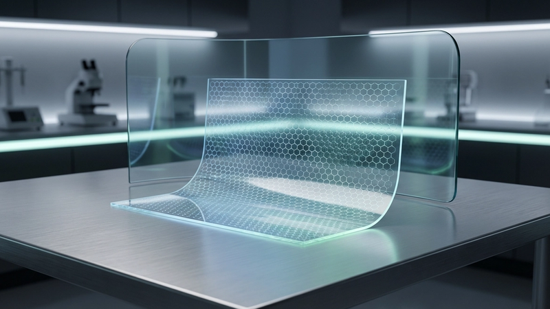
Graphene Transparent Electrodes for Displays
Graphene, a single atomic layer of sp2-hybridized carbon atoms arranged in a hexagonal lattice, presents an unparalleled platform for next-generation transparent electrodes, fundamentally challenging the incumbent indium tin oxide (ITO). Its unique two-dimensional (2D) confinement dictates an electronic band structure characterized by Dirac cones, where electrons and holes behave as massless Dirac fermions. This relativistic-like behavior at low energies results in extraordinary charge carrier mobility, exceeding 200,000 cm^2/Vs in suspended samples at room temperature, and an intrinsic current carrying capacity approaching 10^8 A/cm^2 – orders of magnitude greater than conventional metals. This remarkable electronic transport, coupled with its atomic thinness, endows graphene with exceptional optical transparency, exhibiting a universal absorbance of approximately 2.3% per layer, directly related to the fine structure constant, thereby transmitting ~97.7% of incident light for a monolayer across a broad spectral range. This combination of high electrical conductivity and optical transparency is precisely what is required for high-performance displays, offering a path to overcome the inherent limitations of ITO, such as its brittleness, scarcity of indium, and relatively high processing temperatures.
The physics of graphene confinement is paramount to its functionality as a transparent electrode. The absence of out-of-plane scattering channels contributes to ballistic transport over significant distances, even at ambient temperatures, minimizing energy dissipation. Furthermore, the ability to tune graphene's Fermi level through electrostatic gating or chemical doping allows for precise control over its carrier concentration and, consequently, its sheet resistance. Achieving target sheet resistances of 100-300 Ohm/sq, comparable to or better than ITO, while maintaining high optical transparency is a critical performance metric for display applications. This tunability is not merely theoretical; it is actively exploited in material engineering to optimize the trade-off between conductivity and transparency. For instance, controlled nitrogen or boron doping during chemical vapor deposition (CVD) synthesis can modulate carrier density, shifting the Dirac point and enhancing conductivity without significantly compromising the optical properties of the atomically thin film.
Beyond its electronic and optical characteristics, the 2D nature of graphene confers additional critical advantages for display technology. Its exceptional in-plane thermal conductivity, reported to be as high as ~5000 W/mK, is crucial for efficient heat dissipation from active display pixels, particularly in high-brightness, high-resolution, or high-refresh-rate panels, thereby enhancing device longevity and stability. Moreover, the robust sp2 bonding within the hexagonal lattice imparts extraordinary mechanical strength (tensile strength ~130 GPa) and flexibility, enabling the realization of bendable, foldable, and even stretchable displays – applications where brittle ITO films are inherently unsuitable. Empirical studies demonstrate that the quality and performance of CVD-grown graphene films, often plagued by grain boundaries and defects, can be significantly improved through post-synthesis treatments. For example, rapid thermal annealing using 3000K thermal pulses applied for milliseconds has been shown to reduce sheet resistance by effectively repairing lattice imperfections and improving grain boundary connectivity, pushing the practical performance of large-area graphene electrodes closer to their theoretical limits.
Pulsed Electrical Resistive Carbon Heating vs. CVD (Comparative Analysis)
The established benchmark for high-quality graphene synthesis, particularly for large-area applications, has been Chemical Vapor Deposition (CVD). This method relies on the catalytic decomposition of carbon precursors, such as methane, on metallic substrates like copper or nickel, typically at 900°C to 1100°C under vacuum. While CVD excels in producing crystalline graphene with precise layer control, its architecture presents formidable challenges for transparent electrode integration in displays. High-temperature growth and a metallic catalyst necessitate a complex transfer step to delaminate the graphene onto the target display substrate, such as flexible PET or rigid glass. This transfer, often polymer-assisted, is a primary source of defects including tears, wrinkles, and residual contamination, severely degrading electrical and optical properties. Empirical data consistently show that a single-layer CVD graphene film, exhibiting ~100 Ω/sq sheet resistance on its growth substrate, can surge to 400-800 Ω/sq post-transfer, alongside reduced optical transparency and uniformity. This multi-stage, batch-oriented approach fundamentally increases production costs, reduces yield, and is incompatible with the high-throughput, roll-to-roll manufacturing protocols critical for advanced display technologies.
In stark contrast, Pulsed Electrical Resistive Carbon Heating (PERCH), also known as Flash Joule Heating (FJH) or Flash Graphene synthesis, offers a disruptive, direct, and catalyst-free pathway. This innovative technique exploits the intrinsic electrical resistivity of diverse carbonaceous feedstocks – from amorphous carbon black and graphite to polymers – to induce ultra-high temperature excursions via intense, short-duration electrical pulses. By passing a high-current pulse through a compacted carbon precursor, its internal resistance generates immense ohmic heating, driving temperatures to levels exceeding 3000 K within milliseconds. This rapid thermal shock triggers spontaneous graphitization, converting disordered carbon into few-layer graphene structures. Crucially, PERCH operates under ambient conditions, eliminating vacuum systems, high-purity precursor gases, or expensive metallic catalysts. The process's transient, localized heating minimizes thermal impact on surrounding materials, a critical advantage for direct synthesis onto temperature-sensitive substrates pertinent to display fabrication.
The fundamental divergence in processing mechanisms translates directly into their respective suitability for transparent electrode applications. CVD's reliance on high-temperature, catalyst-mediated growth and the subsequent defect-prone transfer step imposes severe limitations on substrate compatibility and manufacturing throughput, directly compromising transparent electrode performance in terms of power efficiency, signal integrity, and visual fidelity. Conversely, PERCH's ability to directly synthesize graphene from inexpensive carbon precursors in a single, ultrafast step fundamentally bypasses these issues. The rapid, localized heating (e.g., 3000K in milliseconds) allows for direct deposition or conversion on diverse substrates, including flexible polymers like PEN or PET, eliminating the damaging transfer process. This direct synthesis inherently preserves graphene's intrinsic properties, leading to lower sheet resistances (e.g., 50-150 Ω/sq for comparable transparency) and superior mechanical robustness, paramount for durable, high-performance transparent electrodes. Furthermore, the millisecond-scale reaction times and atmospheric pressure operation of PERCH offer a pathway to continuous, high-volume production, significantly reducing energy footprint and capital expenditure compared to energy-intensive, batch-oriented CVD processes. This direct, additive approach, contrasting sharply with CVD's multi-step method, positions PERCH as a pivotal technology for cost-effective, ubiquitous graphene-based transparent electronics.
The Crystallography of Turbostratic Graphene (Why Layer Alignment Matters)
Turbostratic graphene (TG) distinguishes itself from highly oriented pyrolytic graphite (HOPG) and perfectly stacked few-layer graphene by its characteristic lack of long-range crystallographic order between constituent layers. Unlike the well-defined ABAB or ABCABC stacking sequences governed by strong van der Waals forces in graphite, TG layers exhibit random rotational and translational misalignments. This disorder arises primarily from the kinetic-driven formation processes, such as chemical vapor deposition (CVD) on certain substrates or the reduction of graphene oxide (rGO), where individual graphene sheets nucleate and grow with independent orientations before stacking. While each individual layer within a turbostratic stack retains its sp2 hybridized hexagonal lattice, the relative disorientation disrupts the interlayer electronic coupling that is crucial for coherent charge transport across multiple layers. The interlayer spacing in TG is often slightly expanded (e.g., >0.34 nm compared to graphite's 0.335 nm) and less uniform, reflecting the weaker and less ordered van der Waals interactions across these misaligned planes. This structural heterogeneity is fundamental to understanding its functional divergence from ideal graphene.
The crystallographic disorder inherent in turbostratic graphene profoundly impacts its electronic transport properties, a critical consideration for transparent electrode applications. The random rotational stacking angles between layers lead to a significant increase in interlayer scattering and a reduction in effective charge carrier mobility compared to single-layer graphene or epitaxially grown few-layer graphene with defined stacking. Electron transport in TG is often dominated by inter-grain boundaries, defects, and interlayer tunneling across misaligned regions rather than ballistic or quasi-ballistic conduction within perfectly aligned domains. This manifests empirically as higher sheet resistance. For instance, while ideal monolayer graphene exhibits sheet resistances below 100 Ohm/square, turbostratic films, even after optimization, frequently present values in the 200-500 Ohm/square range for comparable optical transparency, often necessitating doping strategies to achieve the sub-100 Ohm/square target for high-performance displays. The phonon scattering mechanisms are also altered, reducing thermal conductivity along the c-axis, which can impact heat dissipation in high-current density electrode applications.
Beyond electronic transport, the turbostratic nature influences optical and mechanical characteristics. While the sp2 carbon network within each layer ensures high intrinsic transparency, the increased density of defects, edge sites, and variations in interlayer spacing across the disordered stack can slightly enhance broadband absorption or introduce scattering centers, potentially reducing the overall optical transmittance at specific wavelengths. Mechanically, the reduced interlayer coherence in TG can lead to a lower effective Young's modulus perpendicular to the layers and altered fracture toughness compared to perfectly ordered graphite, although the in-plane strength of individual graphene sheets remains high. Post-synthesis thermal treatments, such as rapid thermal annealing using focused energy pulses at temperatures up to 3000K for milliseconds, are often employed to partially mitigate turbostratic disorder by promoting local re-crystallization and defect healing, thereby enhancing electrical conductivity and improving adhesion without compromising the film's overall transparency. However, achieving full graphitic order from a turbostratic precursor remains a significant challenge. The myriad edge sites and structural imperfections present in turbostratic graphene also contribute to its high surface area and chemical reactivity, evidenced by its impressive 79% heavy metal adsorption efficiency in environmental applications, a property that, while beneficial elsewhere, necessitates careful passivation for stable electronic device integration.
Industrial Scalability & Commercial Integration Barriers
The industrial scalability of high-quality graphene for transparent electrode applications remains a formidable challenge, primarily revolving around large-area synthesis and defect-free transfer processes. Chemical Vapor Deposition (CVD) on catalytic metal foils, typically copper, yields high-quality monolayer or few-layer graphene but necessitates growth temperatures approaching 1000°C. The subsequent transfer from the growth substrate to the target display substrate (e.g., PET, glass) introduces significant hurdles. Wet transfer methods, while widely studied, often leave behind polymer residues (e.g., PMMA, typically 5-10% residual coverage), create micro-tears, wrinkles, and doping inhomogeneities, thereby compromising both optical transparency and electrical uniformity. Achieving a sheet resistance below 100 Ohm/sq at 90% optical transmittance across meter-scale substrates, crucial for display applications, is difficult due to these transfer-induced defects and grain boundaries inherent to polycrystalline CVD graphene. While nascent roll-to-roll CVD systems promise higher throughput, they still contend with maintaining consistent material quality, minimizing defect density, and ensuring precise alignment over large areas, presenting a significant gap to the established economies of scale seen in indium tin oxide (ITO) sputtering.
Solution-processed graphene, derived from graphene oxide (GO) or reduced graphene oxide (rGO), offers a potentially more scalable and cost-effective pathway, leveraging existing coating techniques such as slot-die or spray coating. However, these methods inherently produce films with higher sheet resistance due to residual oxygen functional groups and poor inter-flake connectivity. Post-processing steps are indispensable to enhance electrical conductivity, commonly involving thermal annealing (e.g., 300-500°C in inert atmosphere) or localized laser reduction. For instance, pulsed laser annealing can generate transient temperatures exceeding 3000K for milliseconds, effectively reducing oxygen content and increasing graphitic domain size, leading to resistivity improvements. Despite these advancements, achieving the high electrical conductivity and low haze required for high-performance transparent electrodes (e.g., <30 Ohm/sq for OLED power delivery) without compromising optical clarity remains a complex optimization problem. Furthermore, the long-term stability of solution-processed films against environmental degradation (e.g., oxidation, humidity) and their mechanical robustness under repeated flexing for flexible displays are critical parameters that demand further research and development to match the performance and reliability of mature ITO.
Commercial integration barriers extend beyond material synthesis and include compatibility with existing display manufacturing infrastructure and cost competitiveness. Patterning graphene films, often achieved via oxygen plasma etching, contrasts with the well-established wet etching processes for ITO, requiring adjustments to fab lines. Adhesion of graphene to diverse display stack materials (e.g., gate dielectrics, organic layers) is another critical factor, as poor interfacial bonding can lead to delamination and device failure. The current cost of producing high-quality, large-area graphene transparent electrodes significantly outweighs that of sputtered ITO, which benefits from decades of process refinement, global supply chains, and high yield rates. Even with superior mechanical flexibility and chemical inertness, the total cost of ownership, including material synthesis, transfer, patterning, and integration, must be dramatically reduced to displace ITO in mainstream display applications. Achieving consistent performance, high manufacturing yields (e.g., >95% for display panels), and long-term reliability under operating conditions comparable to ITO remains the paramount challenge for graphene's commercial viability in this demanding sector.
Economic Feasibility and USA-Made Manufacturing Advantage
The economic feasibility of Graphene Transparent Electrodes (GTEs) for displays is critically tied to overcoming current manufacturing cost drivers. Synthesis via Chemical Vapor Deposition (CVD) on catalytic foils or epitaxial growth on SiC necessitates high-temperature processes, often exceeding 1000°C for CVD and 1500-2000°C for SiC, incurring significant energy expenditure and capital costs. The multi-step transfer of graphene from growth substrate to display substrate is a major contributor to cost, defect density, and non-uniformity across meter-scale panels. While precursors like methane are cheaper than indium, their scale-up costs are non-trivial. Incumbent Indium Tin Oxide (ITO) manufacturing, despite maturity, grapples with indium scarcity, price volatility, and energy-intensive vacuum deposition. GTE cost reduction hinges on transitioning to continuous, high-throughput methods like roll-to-roll (R2R) CVD or atmospheric pressure CVD (APCVD) on flexible substrates. These promise substantial reductions in processing time and cost per unit area. Lower-temperature synthesis methods (e.g., plasma-enhanced CVD below 500°C) and direct growth techniques eliminating transfer are crucial for cost parity. Doping innovations to achieve sheet resistances below 10 Ohm/sq with minimal optical absorption are paramount, reducing required graphene layers and associated material/processing costs.
Graphene's intrinsic properties offer a compelling performance-to-cost ratio, transcending mere manufacturing expense. A single-layer graphene film exhibits optical transparency exceeding 97.7% in the visible spectrum, superior to typical ITO films which often show absorption losses. Electrically, doped graphene can achieve sheet resistances as low as 5-10 Ohm/sq while maintaining high transparency, crucial for large-format, high-resolution displays. Critically, graphene's exceptional mechanical flexibility, withstanding millions of bending cycles at a 1 mm
Future Horizons & High-Value B2B Applications
The advent of graphene as a transparent electrode extends beyond direct indium tin oxide (ITO) replacement, ushering in capabilities for truly flexible, foldable, and even stretchable display architectures. Graphene’s intrinsic properties, including its exceptional mechanical strength (Young's modulus ~1 TPa, tensile strength ~130 GPa), atomic thinness, and high optical transparency (97.7% for a single layer), are foundational to these advancements. Achieving commercial viability necessitates overcoming challenges in large-area, defect-free graphene transfer onto flexible substrates such as PEN, PET, or polyimide, with roll-to-roll chemical vapor deposition (CVD) emerging as a leading scalable manufacturing technique. For these applications, maintaining a stable sheet resistance below 100 Ohm/sq after 100,000 bending cycles at a 1mm radius is a critical performance metric, ensuring device longevity and reliability in dynamic use cases. Furthermore, graphene’s high surface-to-volume ratio and electrical sensitivity facilitate the integration of advanced transparent sensors directly within the display stack, enabling sophisticated multi-touch, pressure-sensing, and even bio-sensing functionalities without compromising visual fidelity.
For high-value B2B applications in next-generation displays, particularly augmented reality (AR) and virtual reality (VR) microdisplays, graphene offers distinct advantages. The stringent requirements for ultra-high pixel densities (e.g., 2000+ pixels per inch), low latency, and rapid refresh rates demand electrode materials with superior electron mobility; graphene’s electron mobility, potentially exceeding 200,000 cm^2/Vs at room temperature, is critical for achieving faster pixel addressing and switching speeds compared to conventional materials. Concurrently, thermal management becomes paramount in densely packed micro-LED or OLED arrays, where localized heating can severely degrade performance and lifetime. Graphene's extraordinary in-plane thermal conductivity, approximately 5000 W/mK, provides an unparalleled heat dissipation pathway, preventing thermal runaway and ensuring uniform luminance across the display. Beyond active displays, graphene’s Fermi level tunability opens avenues for dynamic optical modulation in smart windows or privacy glass, enabling electrochromic or thermochromic functionalities with response times in the low tens of milliseconds and significantly reduced power consumption compared to existing solutions.
The future commercialization of graphene transparent electrodes hinges on achieving large-scale, cost-effective manufacturing and seamless integration into existing display fabrication workflows. Current research focuses on advancing roll-to-roll atmospheric pressure CVD for producing large-area graphene films (e.g., compatible with Gen 8 display substrates) and reducing production costs to compete economically with ITO, mitigating concerns over indium scarcity. To meet the performance demands of high-brightness, large-format displays, hybrid transparent conductor architectures, such as graphene-metal nanowire networks or graphene-PEDOT:PSS composites, are being explored to achieve ultra-low sheet resistances below 5 Ohm/sq while maintaining optical transmittances exceeding 90% across the visible spectrum. Precise patterning techniques, including selective laser ablation or advanced photolithography, are under continuous development to ensure the structural integrity and electrical performance of graphene electrodes post-processing. Moreover, graphene's chemical inertness and barrier properties position it as an ideal robust electrode for emerging display technologies like quantum dot light-emitting diodes (QLEDs) and perovskite light-emitting diodes (PeLEDs), enhancing their long-term stability and operational lifetime, particularly in flexible form factors or challenging environmental conditions. Its resilience to localized thermal pulses, for instance, tolerating temperatures up to 3000K during rapid annealing of underlying layers, provides a significant processing window advantage.
Evaluate Our Quality
Serious about B2B integration? Test our premium Pulsed Electrical Resistive Carbon Heating turbostratic graphene in your lab. 100g sample packs available now.