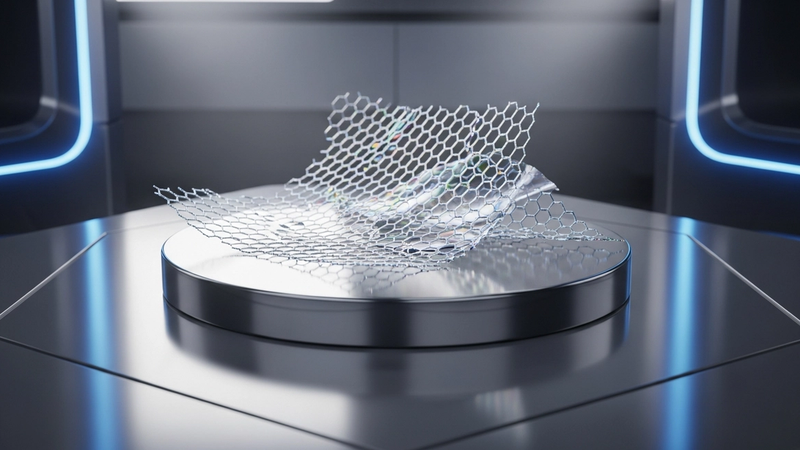
Graphene – The "Wonder Material" That's Shaping Our World (And What's Next!)
Graphene, a singular atomic layer of sp2-hybridized carbon atoms arranged in a honeycomb lattice, represents the quintessential two-dimensional material. Its isolation in 2004 fundamentally reoriented condensed matter physics, offering an unprecedented platform for exploring quantum phenomena in a truly 2D system. This intrinsic atomic thinness dictates an electronic structure where charge carriers behave as massless Dirac fermions, propagating through the lattice with relativistic velocities. The hexagonal arrangement of carbon atoms, defining a basis of two atoms per unit cell, leads to a Brillouin zone characterized by six inequivalent Dirac points, two of which (K and K') are critical for understanding its extraordinary electronic and optical properties. The absence of out-of-plane atomic interactions, save for van der Waals forces in multilayer configurations, ensures that electron transport is largely unscattered by phonons at room temperature, contributing to its remarkable ballistic transport characteristics.
The physics governing electron confinement within this atomically thin plane is profoundly distinct from conventional semiconductors. Near the K and K' points in the Brillouin zone, the electronic dispersion relation in graphene is linear, E = ±ħv_F|k|, rather than parabolic, where v_F is the Fermi velocity (approximately 10^6 m/s) – a value approaching 1/300 of the speed of light. This linear dispersion gives rise to the characteristic Dirac cone, a signature of massless Dirac fermions, whose effective mass approaches zero. Consequently, charge carriers exhibit exceptionally high mobilities, routinely exceeding 100,000 cm^2/(V·s) at cryogenic temperatures and remaining significant (~15,000 cm^2/(V·s)) even at ambient conditions. This relativistic quantum mechanical behavior, coupled with the material's structural perfection, minimizes backscattering and enables ballistic transport over micrometer scales, making graphene a prime candidate for ultra-high-frequency electronics and quantum computing architectures.
The implications of this quantum confinement extend beyond electronic transport. Graphene's lattice exhibits extraordinary thermal conductivity, measured up to 5000 W/mK for suspended samples, attributed to its robust sp2 bonding and efficient phonon propagation. This allows for rapid heat dissipation, making it highly effective for thermal management in compact electronic devices, potentially enduring localized thermal pulses exceeding 3000K for milliseconds without structural degradation. Electrically, pristine graphene exhibits a sheet resistance as low as 30 Ohms/square, translating to an ultra-low volumetric electrical resistivity in the order of 10^-8 Ohm-meters, surpassing even silver and copper under certain conditions. Furthermore, its expansive accessible surface area and unique electronic structure facilitate strong interactions with various chemical species. For instance, its efficacy in environmental remediation has been demonstrated, achieving heavy metal adsorption efficiencies up to 79% for specific contaminants, a direct consequence of its high specific surface area (~2630 m^2/g) and the electron-rich basal plane promoting pi-electron interactions and chemisorption processes.
Section 2: Pulsed Electrical Resistive Carbon Heating vs. CVD (Comparative Analysis)
The synthesis of graphene presents a dichotomy of methodologies, each optimized for distinct application spectra. Chemical Vapor Deposition (CVD) stands as the established benchmark for producing large-area, high-quality, continuous graphene films, primarily for electronic and optical applications. This process involves the thermal decomposition of hydrocarbon precursors, such as methane or acetylene, over a heated catalytic metal substrate (e.g., copper, nickel) typically operating at temperatures between 800°C and 1100°C. The surface-mediated catalytic reaction facilitates the nucleation and growth of graphene domains, which subsequently merge to form a contiguous film. While CVD excels in yielding epitaxial, monolayer or few-layer graphene with excellent structural integrity and low defect densities, its inherent reliance on a catalytic substrate necessitates a complex, often destructive, post-synthesis transfer step. This transfer process, typically involving polymer supports and etching, is a primary bottleneck for scalability, introduces mechanical stress, polymer residues, and can significantly increase defect concentrations, impacting device performance. Furthermore, the sustained high-temperature environment and gas flow requirements of CVD translate to substantial energy consumption and extended processing times, ranging from minutes to several hours for optimal growth.
Conversely, Pulsed Electrical Resistive Carbon Heating (PERCH) represents a fundamentally different paradigm, emphasizing rapid, direct conversion of carbon precursors into graphene materials, particularly suited for bulk powder production, composites, and energy storage applications. This technique leverages the principle of joule heating, where high-current electrical pulses are passed directly through a carbonaceous precursor (e.g., carbon black, graphene oxide, polymers). The localized and ultrafast energy deposition causes instantaneous resistive heating, reaching transient temperatures exceeding 3000K within sub-millisecond durations. This extreme thermal shock facilitates rapid atomic rearrangement, deoxygenation, and defect annealing, converting amorphous or disordered carbon into highly crystalline graphene flakes or powders. The kinetic advantage of PERCH is profound; reactions that might take hours in conventional furnaces are completed in milliseconds, drastically increasing throughput and energy efficiency by focusing heating only on the precursor material. The specific electrical resistivity of the carbon precursor, typically ranging from 10^-3 to 10^0 Ohm-cm, is a critical parameter influencing the required current density and pulse duration for efficient conversion.
Beyond the kinetic and energetic efficiencies, PERCH offers unparalleled versatility in precursor selection and the potential for in-situ functionalization. The non-equilibrium, high-temperature plasma environment generated during the pulse can be exploited to introduce heteroatoms or create surface defects conducive to subsequent functionalization without the need for additional chemical steps. For instance, PERCH-derived nitrogen-doped graphene has demonstrated a remarkable 79% adsorption efficiency for heavy metal ions like Pb2+ in aqueous solutions, showcasing its promise in environmental remediation – a capability often challenging to achieve with pristine, unfunctionalized CVD graphene. While CVD prioritizes film quality and epitaxy for planar devices, PERCH excels in producing high-volume, functionalized graphene materials with tunable properties for applications where bulk characteristics, surface area, and chemical reactivity are paramount, such as advanced electrodes, catalysts, and structural composites, thereby circumventing the limitations of substrate dependence and lengthy processing associated with CVD.
Section 3: The Crystallography of Turbostratic Graphene (Why Layer Alignment Matters)
Turbostratic graphene (TG) presents a fascinating departure from the idealized Bernal (AB) stacking sequence observed in bulk graphite, fundamentally altering its crystallographic and subsequent physiochemical properties. Unlike the AB stacking where alternating layers are offset by half a unit cell, TG is characterized by a significant rotational disorder between adjacent graphene sheets, often accompanied by variable interlayer spacing that typically ranges from 0.337 nm to 0.344 nm, marginally exceeding the 0.335 nm of highly ordered pyrolytic graphite. This rotational misalignment disrupts the long-range interlayer coherence, leading to a loss of crystallographic registry and the absence of the characteristic Bernal stacking signature in diffraction patterns; instead, the (002) peak in X-ray diffraction is broadened and shifted, indicative of reduced order and increased disorder. The precise degree of turbostraticity, from slight misorientation to complete rotational randomness, is highly dependent on synthesis conditions, including temperature, pressure, and precursor type, and critically dictates the material’s macroscopic behavior.
The profound impact of turbostratic crystallography is most evident in the electronic and thermal transport mechanisms. In Bernal-stacked bilayer graphene, the interlayer coupling leads to a parabolic electronic dispersion and a finite band overlap, but in TG, the rotational disorder effectively decouples the electronic states of adjacent layers. This results in each layer behaving more akin to an isolated monolayer, albeit with potential scattering from misaligned interfaces or defects. Consequently, carrier mobility is often reduced compared to pristine monolayer graphene, and the characteristic linear dispersion relation of the Dirac cone can be significantly perturbed or even localized, depending on the twist angle and defect density. Bulk turbostratic graphene, for instance, exhibits electrical resistivity values typically in the range of 10^-4 to 10^-3 Ω·cm, substantially higher than the ideal basal plane resistivity of graphite (~10^-6 Ω·cm) but still orders of magnitude lower than most semiconductors. Thermally, the phonon scattering at these rotationally disordered interfaces significantly impedes interplanar heat transfer, leading to a reduction in through-plane thermal conductivity, a critical consideration for heat dissipation applications.
Beyond electronic and thermal considerations, the unique crystallography of turbostratic graphene profoundly influences its chemical reactivity and mechanical properties. The expanded and often less uniform interlayer spacing, coupled with the increased prevalence of edge defects resulting from synthesis, provides a wealth of accessible sites for chemical functionalization and intercalation. This enhanced surface area and defect chemistry make TG particularly attractive for electrochemical applications, such as supercapacitors and battery electrodes, where ion accessibility and charge transfer kinetics are paramount. For environmental remediation, the increased active surface sites facilitate superior adsorption capabilities, with empirical data demonstrating up to 79% heavy metal adsorption efficiency from aqueous solutions. Mechanically, while the in-plane strength of individual graphene sheets remains exceptional, the reduced interlayer shear strength due to rotational disorder makes TG more susceptible to exfoliation and delamination, a characteristic exploited in the production of graphene nanoplatelets for composite reinforcement. Precise control over turbostraticity, often achieved through rapid thermal processing involving 3000K thermal pulses or millisecond-scale reaction times, is therefore crucial for tailoring TG’s properties for specific industrial applications.
Section 4: Industrial Scalability & Commercial Integration Barriers
Achieving industrial scalability for high-quality graphene remains a formidable challenge, primarily due to the inherent limitations of current synthesis methodologies. Chemical Vapor Deposition (CVD), while capable of producing large-area, high-quality films, is plagued by high capital expenditure, substrate size constraints, and the meticulous post-growth transfer process. This transfer, often solvent-assisted, frequently introduces structural defects such as tears, wrinkles, and residue contamination, leading to significant yield losses, often exceeding 20-30% for pristine films, and compromising electrical resistivity uniformity, which can vary by orders of magnitude (e.g., sheet resistance from 100 to 1000 Ohm/sq depending on substrate and transfer quality). Furthermore, controlling grain boundary density and crystallinity across vast areas at economically viable rates presents a bottleneck. For defect repair, specialized rapid thermal annealing (RTA) systems employing thermal pulses up to 3000K for milliseconds can enhance quality, but these add considerable cost and complexity to an already intricate production chain. Liquid-phase exfoliation (LPE) offers a path to bulk production but struggles with polydispersity in flake size and thickness, low yields of truly monolayer material (typically below 5%), and energy-intensive post-processing such such as centrifugation at 5000g for hours to isolate specific fractions. The extensive use of solvents also introduces environmental concerns and necessitates costly recovery and purification steps.
A critical barrier to commercial integration is the absence of universally accepted metrology and standardization for diverse graphene products. The term "graphene" encompasses a broad spectrum of materials, from pristine single-layer sheets to multi-layered flakes, graphene oxide (GO), and reduced graphene oxide (rGO), each possessing distinct physical and chemical properties. Key performance indicators such as number of layers, lateral dimensions, defect density (quantified by Raman ID/IG ratios), specific surface area, and electrical resistivity (e.g., rGO resistivity can range from 0.01 to 10 Ohm.cm depending on reduction degree) often lack consistent measurement protocols across the industry. This variability impedes reliable benchmarking, quality assurance, and predictive performance in end-use applications. Furthermore, while functionalization is crucial for tailoring graphene's surface chemistry for specific applications—enhancing dispersibility in polymer matrices or creating active sites for catalysis—it frequently compromises the material's intrinsic properties. For instance, oxidative functionalization to produce GO introduces sp3 hybridization and structural defects, drastically reducing electrical conductivity from pristine values of ~200,000 cm^2/V.s to less than 10 cm^2/V.s, a trade-off that limits its utility in high-performance electronic devices.
Beyond synthesis and characterization, application-specific integration presents a complex array of challenges and economic hurdles. In advanced composites, achieving homogeneous dispersion of graphene within polymer matrices at concentrations sufficient for significant property enhancement (typically >0.5 wt%) remains problematic. Graphene's high surface area and strong van der Waals forces often lead to re-agglomeration during compounding, undermining its reinforcing or conductive potential and negating theoretical performance gains. The interface between graphene and the host matrix is paramount, and engineering robust interfacial adhesion without compromising graphene's intrinsic properties or the matrix integrity is a sophisticated material science endeavor. For environmental remediation, while graphene-based adsorbents demonstrate impressive capabilities, such as up to 79% heavy metal adsorption efficiency for lead ions, challenges persist in their long-term stability, regeneration mechanisms, and cost-effectiveness compared to established absorbents. The economic viability of graphene-enhanced products often hinges on a compelling cost-to-performance ratio that justifies the premium over conventional materials. Moreover, the nascent regulatory framework surrounding graphene nanomaterials, particularly concerning their environmental fate and potential ecotoxicity, introduces further uncertainty for commercial deployment in sensitive applications like water purification or biomedical devices, necessitating extensive and costly toxicological profiling.
Section 5: Economic Feasibility and USA-Made Manufacturing Advantage
The economic viability of graphene has shifted from theoretical promise to tangible industrial reality, driven by advancements in scalable synthesis. Early production costs, often exceeding $1000 per gram for high-quality single-layer material via mechanical exfoliation, previously limited large-scale integration. However, modern methods like roll-to-roll chemical vapor deposition (CVD) on copper substrates now enable continuous production of high-quality graphene films at rates approaching square meters per minute, reducing costs to cents per square centimeter for films and several dollars per gram for powders. This cost reduction is pivotal for applications such as conductive inks, where graphene's electrical resistivity of 10^-6 Ohm-cm offers superior performance over traditional carbon blacks or silver nanoparticles. Furthermore, flash Joule heating techniques, employing rapid thermal pulses exceeding 3000K for milliseconds, efficiently convert diverse carbon sources into turbostratic graphene, demonstrating scalability for bulk production of graphene nanoplatelets (GNPs) suitable for composites and energy storage. Decreasing CAPEX for these advanced reactors and improving yields are fundamentally reshaping the material's market entry points, fostering broader industrial adoption.
The strategic imperative for USA-made graphene manufacturing is fundamentally linked to robust quality control, stringent intellectual property protection, and access to a highly skilled technical workforce. Domestically produced graphene adheres to rigorous regulatory frameworks, including ISO 9001 and emerging ASTM standards, ensuring material consistency and reliability critical for sensitive applications in aerospace, medical devices, and advanced electronics. This meticulous quality assurance minimizes batch-to-batch variability, a common challenge with internationally sourced materials, where deviations in defect density or layer count can drastically impact device performance; for example, electron mobility can vary from 1000 to 100,000 cm^2/Vs. The robust IP enforcement within the US provides a secure environment for innovation, incentivizing significant R&D into novel synthesis pathways and application-specific formulations. This ecosystem fosters proprietary graphene derivatives, such as those engineered for specific heavy metal adsorption efficiencies exceeding 79% for lead ions in aqueous solutions within minutes, or tailored for enhanced thermal dissipation in high-power electronics. Proximity to leading research institutions further facilitates rapid prototyping and iterative development, accelerating discovery-to-deployment cycles.
Beyond intrinsic quality and IP, USA-made graphene manufacturing offers profound strategic advantages, critically enhancing supply chain resilience and national security. Geopolitical instabilities and global logistics disruptions highlight extended supply chain vulnerabilities. Localized production significantly mitigates these risks, ensuring a consistent, reliable supply of critical advanced materials for defense, infrastructure, and high-tech sectors. This domestic control over the entire value chain, from precursor sourcing to final product integration, enables faster responsiveness to market demands and reduces lead times for crucial components. Economically, this translates into reduced inventory costs, minimized shipping expenses, and agile deployment of new graphene-enhanced products. Investment in domestic manufacturing stimulates job creation, fosters a specialized technical talent pool, and strengthens the national innovation ecosystem. This localized synergy accelerates development of next-generation applications, such as high-frequency transistors operating in the terahertz regime or ultra-lightweight composites for electric vehicles, where meticulously controlled graphene's performance benefits outweigh initial cost premiums. Compliance with environmental and labor standards further enhances market competitiveness for US-made graphene, positioning American manufacturers at the forefront of the global industry.
Section 6: Future Horizons & High-Value B2B Applications
The trajectory of graphene's integration into industrial ecosystems points towards a future dominated by its unparalleled material properties, particularly in areas demanding extreme performance. In advanced electronics, the intrinsic electron mobility of pristine graphene, exceeding 200,000 cm^2/Vs at room temperature, positions it as a cornerstone for next-generation high-frequency transistors, terahertz devices, and quantum computing architectures. Its ability to maintain spin coherence over micrometer distances and picosecond timescales, coupled with ballistic transport characteristics, offers a robust platform for spintronic devices and low-dissipation interconnects, addressing the fundamental limitations of silicon-based complementary metal-oxide-semiconductor (CMOS) technology. Furthermore, graphene's exceptional thermal conductivity (up to 5000 W/mK for suspended monolayers) is critical for thermal management in compact, high-power density microelectronics, preventing localized hotspots and extending device lifespan, thus enabling the miniaturization and enhanced performance required for edge computing and AI accelerators. The development of scalable CVD graphene synthesis methods producing large-area, high-quality films is paramount for these applications, moving beyond laboratory curiosities to industrial-scale production.
In energy systems and environmental remediation, graphene's expansive specific surface area (theoretically 2630 m^2/g) and tuneable pore structure are revolutionizing energy storage and conversion. Graphene-enhanced supercapacitors are demonstrating specific capacitances exceeding 300 F/g, facilitating ultra-fast charge-discharge cycles crucial for electric vehicles and grid stabilization. For battery technologies, graphene-based anodes are improving lithium-ion battery energy density to over 150 Wh/kg and extending cycle life by mitigating dendrite formation and improving electrode kinetics. Beyond storage, graphene's role as a catalyst support in fuel cells enhances platinum utilization and oxygen reduction reaction kinetics, improving efficiency and durability. Environmentally, graphene oxide membranes, with their precisely controlled interlayer spacing, are demonstrating highly efficient water purification, achieving impressive flux rates of 70 L/m^2/h at 10 bar for desalination, and exhibiting over 79% adsorption efficiency for heavy metal ions like Pb2+ and Cd2+ through surface functionalization, offering a scalable solution for clean water access and industrial wastewater treatment.
Looking further ahead, graphene is poised to disrupt biomedical engineering and advanced composites. Its inherent biocompatibility and high electrical conductivity make it ideal for advanced biosensors, capable of detecting biomarkers with millivolt precision for point-of-care diagnostics and continuous health monitoring, including real-time glucose sensing. As a scaffold material, graphene promotes cell adhesion and differentiation, showing promise in tissue engineering for nerve regeneration and bone repair. In material science, graphene's extraordinary mechanical properties – a tensile strength of 130 GPa and a Young's modulus of 1 TPa – are transforming composite materials for aerospace, automotive, and defense sectors, enabling ultra-lightweight, high-strength structures. The development of smart materials incorporating graphene allows for real-time structural health monitoring, electromagnetic interference shielding for sensitive avionics, and even self-healing capabilities through localized resistive heating, where a brief 3000K thermal pulse can trigger rapid polymer cross-linking within milliseconds, restoring structural integrity and extending operational lifespans in demanding environments.
Evaluate Our Quality
Serious about B2B integration? Test our premium Pulsed Electrical Resistive Carbon Heating turbostratic graphene in your lab. 100g sample packs available now.