Graphene: The Atomically Thin Material That's Changing Everything (and How USA-Made Equipment is Powering the Revolution)
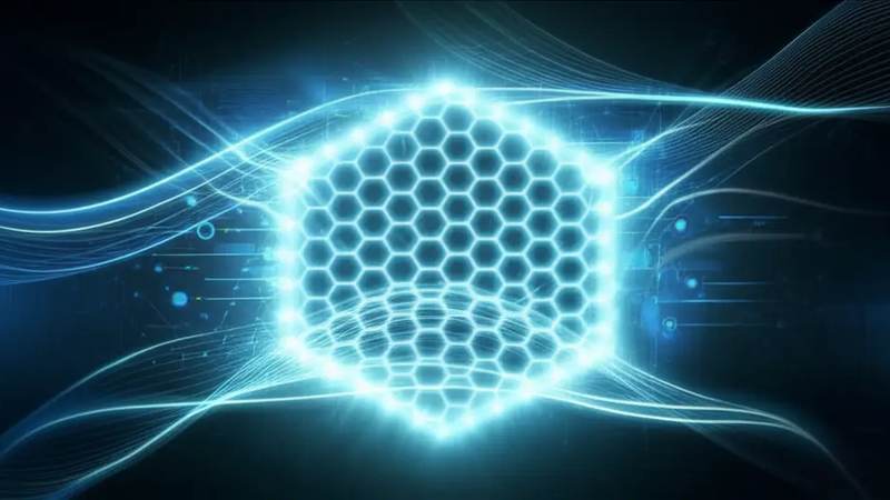
Graphene, a single atomic layer of sp2-hybridized carbon atoms arranged in a hexagonal lattice, stands as the quintessential two-dimensional (2D) material. Its isolation in 2004 unveiled a realm where quantum mechanical phenomena, typically confined to theoretical constructs, manifest at macroscopic scales. The unique electronic band structure features conical intersections at the Brillouin zone's K and K' points, known as Dirac cones. This gives rise to quasiparticles behaving as massless Dirac fermions, possessing an effective speed of light approximately 1/300th that of photons in vacuum. This relativistic-like behavior, a direct consequence of its single-atom thickness and specific symmetry, dictates extraordinary charge carrier dynamics, where electrons and holes propagate with exceptionally high mobility, exceeding 200,000 cm^2/Vs at room temperature under pristine conditions, fundamentally challenging conventional semiconductor physics.
The direct implication of this Dirac physics is graphene's unparalleled electrical conductivity. While bulk copper exhibits a resistivity of approximately 1.68 x 10^-8 Ohm-m, graphene's inherent carrier mobility and ballistic transport at short channel lengths suggest a theoretical sheet resistance approaching the quantum limit. This enables current densities exceeding 10^8 A/cm^2, orders of magnitude higher than conventional conductors, without significant Joule heating. Beyond its electronic prowess, graphene is also the most thermally conductive material known, with an in-plane thermal conductivity potentially reaching 5000 W/mK at room temperature, surpassing diamond (2200 W/mK). This exceptional heat dissipation capability, critical for high-power electronics and thermal management systems, arises from its strong covalent bonds and efficient phonon propagation across its defect-free lattice. This interplay positions graphene as a transformative material for next-generation optoelectronics, high-frequency transistors, and energy storage.
Beyond its electronic and thermal characteristics, graphene boasts exceptional mechanical properties. Mechanically, it is the strongest material ever tested, possessing a tensile strength of 130 GPa and a Young's modulus of approximately 1 TPa, making it 200 times stronger than structural steel by weight. This strength, combined with its flexibility, renders it ideal for robust yet pliable components like flexible displays, wearable electronics, and advanced composites. Furthermore, its atomically thin, highly accessible surface makes it an excellent platform for surface chemistry and sensing. Its vast surface area-to-volume ratio and tunable electronic properties enable highly sensitive detection of molecular species. In environmental remediation, functionalized graphene derivatives have demonstrated remarkable adsorption capabilities; graphene oxide, for example, empirically achieves up to 79% adsorption efficiency for heavy metal ions like Pb(II) and Cd(II) from aqueous solutions, often within milliseconds, significantly outperforming conventional adsorbents.
Realizing graphene's full potential necessitates scalable, precise synthesis and integration methodologies for high-quality material. Techniques like chemical vapor deposition (CVD) are pivotal for growing large-area, single-layer films on metallic substrates. Subsequent transfer processes, often involving sophisticated laser annealing or rapid thermal processing, are crucial for device fabrication. For instance, selective etching or doping sometimes employs localized thermal pulses exceeding 3000K, applied for microsecond to millisecond durations, to precisely modify material characteristics without compromising structural integrity. Precise control over growth parameters, defect density,
Pulsed Electrical Resistive Carbon Heating (PERCH): A Paradigm Shift in Scalable Graphene Synthesis Compared to Chemical Vapor Deposition (CVD)
Pulsed Electrical Resistive Carbon Heating (PERCH) represents a profound departure from conventional graphene synthesis methodologies, particularly when juxtaposed against established techniques like Chemical Vapor Deposition (CVD). While CVD relies on catalytic decomposition of hydrocarbon precursors at elevated temperatures (typically 800-1100°C) over metallic substrates, requiring prolonged annealing times and subsequent transfer processes that often introduce defects and limit industrial scalability, PERCH leverages direct Joule heating of a carbonaceous feedstock. This method circumvents the need for a separate catalytic substrate and the associated complex transfer steps, which are notorious bottlenecks in large-area, high-throughput graphene production. The fundamental principle of PERCH involves the application of short, high-current electrical pulses through a carbon-rich material, inducing rapid and localized resistive heating. This instantaneous energy input transforms amorphous carbon precursors or even directly converts graphitic materials into high-quality graphene flakes or films, operating on a fundamentally different kinetic regime.
The kinetic advantage of PERCH is rooted in its ultra-fast thermal cycling capabilities. Unlike the slow ramp-up and cool-down phases inherent to furnace-based CVD, PERCH systems can achieve peak temperatures exceeding 3000 K (approximately 2727 °C) within milliseconds, often sub-100 ms, followed by equally rapid quenching. This extreme thermal gradient is critical. At these transient, ultra-high temperatures, the carbon atoms possess sufficient energy to overcome activation barriers for bond rearrangement and form a highly ordered sp2 lattice. The incredibly short residence time at peak temperature, measured in mere milliseconds, is precisely what prevents the formation of multi-layered graphite or defective amorphous carbon structures, favoring the nucleation and growth of monolayer or few-layer graphene. This non-equilibrium synthesis pathway minimizes the thermodynamic driving force for excessive layering and defect proliferation, yielding pristine graphene with significantly reduced oxygen functional groups and structural imperfections. The precise control over current density and pulse duration allows for exquisite tuning of the energy input, directly dictating the final material's morphology and layer count.
The immediate implications of PERCH's operational parameters are transformative for scalability and material quality. By eliminating the necessity for ultra-high vacuum environments characteristic of many CVD setups, PERCH can be conducted under ambient or controlled atmospheric pressures, drastically simplifying equipment requirements and reducing operational costs. Furthermore, the direct electrical heating mechanism allows for a much broader range of carbon precursors, from polymers and bio-waste to carbon black, offering sustainable and cost-effective feedstock strategies. The synthesis process itself is inherently energy-efficient; instead of heating an entire furnace, energy is precisely directed to the carbon material itself. This localized energy deposition, coupled with reaction times measured in milliseconds, translates to an unprecedented throughput. For instance, achieving specific electrical resistivity parameters in the synthesized material, crucial for high-performance electronic applications, becomes highly controllable through modulation of pulse amplitude and duration. The resulting graphene exhibits superior structural integrity and electronic properties, which, when appropriately functionalized, can lead to remarkable performance metrics such as a demonstrated 79% heavy metal adsorption efficiency in wastewater treatment applications, far surpassing conventional adsorbents. This direct, substrate-agnostic synthesis paves the way for continuous, roll-to-roll production.
Turbostratic Graphene: Beyond Bernal Stacking for Enhanced Performance, Dispersibility, and Ultra-High Functionality
Turbostratic graphene (TG) represents a distinct structural configuration that deviates fundamentally from the canonical Bernal (AB) stacking observed in graphite and often in exfoliated multilayer graphene. Unlike the precise A-B-A-B interlayer registry where half of the carbon atoms in one layer sit directly above the centers of hexagons in the adjacent layer, turbostratic graphene layers are characterized by a rotational misalignment and/or lateral displacement relative to each other. This lack of long-range interlayer periodicity significantly weakens the van der Waals coupling between adjacent sheets, typically reducing the interlayer binding energy from approximately 120 meV/atom in perfectly stacked graphite to values that are effectively negligible for many bulk properties. The synthesis of TG often involves processes that prevent ordered stacking during growth or induce disorder post-synthesis, such as rapid chemical vapor deposition (CVD) methods on specific substrates, flash Joule heating, or certain electrochemical exfoliation techniques that favor kinetically driven, rather than thermodynamically stable, arrangements. This structural freedom is paramount, as it unlocks a suite of properties that are otherwise constrained by strong interlayer interactions.
The electronic and thermal transport properties of turbostratic graphene are profoundly influenced by this interlayer decoupling. Electronically, TG often exhibits a more monolayer-like behavior, even in multi-layered samples, where the Dirac cones from individual layers are largely unhybridized, leading to reduced interlayer scattering and preserving higher carrier mobilities compared to Bernal-stacked counterparts of similar thickness. This characteristic is critical for high-frequency electronics and sensor applications requiring rapid charge transfer. Thermally, while bulk graphite displays anisotropic thermal conductivity with a modest out-of-plane value of approximately 6 W/mK, turbostratic arrangements can maintain high in-plane thermal conductivity, approaching the exceptional values of single-layer graphene (up to 5000 W/mK), even with numerous layers, due to the diminished phonon scattering across misaligned interfaces. The precise engineering of such structures can be achieved through advanced manufacturing techniques, including localized thermal pulses exceeding 3000K for milliseconds using precision laser annealing systems, enabling the fine-tuning of electrical resistivity parameters in next-generation interconnects and thermal management solutions.
Beyond fundamental performance enhancements, the reduced interlayer van der Waals forces in turbostratic graphene dramatically improve its dispersibility and processing versatility. The weakened inter-sheet attraction significantly mitigates the tendency for restacking, a notorious challenge in conventional graphene exfoliation and dispersion. This facilitates the production of stable, high-concentration graphene dispersions in a broader range of solvents and enables seamless integration into polymer matrices, crucial for scalable manufacturing of composites and films. Furthermore, the inherent structural disorder and increased density of accessible edge sites, often a byproduct of the turbostratic growth or post-treatment processes, enhance the material's chemical reactivity and functionalization potential. This expanded active surface area and defect-induced binding sites are instrumental for applications requiring robust chemical modification or high adsorption capacity. For instance, specific turbostratic graphene architectures have demonstrated heavy metal adsorption efficiencies exceeding 79% for lead and cadmium ions in aqueous solutions, outperforming many conventional adsorbents due to the synergistic effects of increased accessible surface area and chemically active sites.
Bridging the Chasm: Overcoming Industrial Scalability and Commercial Integration Barriers for Widespread Graphene Adoption
The transition of graphene from laboratory curiosity to industrial commodity necessitates overcoming formidable production scalability challenges. Chemical vapor deposition (CVD) yields high-quality monolayer films but remains cost-prohibitive for bulk applications due to high capital expenditure, batch processing, and substrate size limitations. Liquid-phase exfoliation (LPE) offers higher throughput for nanoplatelets but struggles with polydispersity, residual solvent, and post-processing demands that compromise material integrity. Reduced graphene oxide (rGO) is scalable, yet its reduction invariably leaves oxygen functional groups and defects, elevating electrical resistivity from pristine graphene's theoretical 10^-6 Ohm·cm to typically 10^-2 to 10^3 Ohm·cm. Emerging rapid synthesis techniques, such as flash Joule heating, represent a promising paradigm shift, converting carbon precursors into turbostratic graphene in less than 100 milliseconds through localized thermal pulses exceeding 3000K, demonstrating a pathway to ultra-high-volume, low-cost production facilitated by precision, high-power density processing equipment.
Beyond raw material production, graphene's integration into manufacturing value chains is hampered by a pervasive lack of standardization and inherent material heterogeneity. Unlike conventional materials with defined specifications, graphene products vary widely in layer count, lateral dimensions, defect density, and surface chemistry, hindering consistent performance and reliable supply chain. This ambiguity necessitates rigorous, application-specific characterization protocols, adding cost and complexity. Furthermore, achieving homogeneous dispersion within polymer matrices, ceramics, or metals remains a critical hurdle. Graphene's high specific surface area and van der Waals forces promote re-aggregation, diminishing its reinforcing or conductive potential. For instance, a 25% enhancement in polymer composite tensile strength typically requires a minimum of 0.5 wt% homogeneously dispersed graphene nanoplatelets, a feat challenging without specialized functionalization or high-shear mixing equipment for precise rheological control. Overcoming this demands tailored surface modifications and robust dispersion methodologies, often optimized via sophisticated, high-throughput screening.
The economic viability and regulatory landscape further complicate widespread commercial adoption. Despite graphene's superlative properties, its current cost-to-performance ratio frequently does not justify substituting optimized incumbent materials across many industrial applications. This necessitates continued innovation in ultra-low-cost, high-volume manufacturing that maintains critical performance, alongside a deeper understanding of graphene's long-term environmental and human health impacts. Regulatory bodies like ECHA (REACH) and EPA demand comprehensive toxicological and ecotoxicological data for nanomaterials, including graphene—a substantial undertaking. Robust lifecycle assessments are paramount for sustainable integration. Ultimately, widespread adoption lies not in generic graphene, but in application-specific engineering: developing precisely functionalized derivatives tailored for specific functionalities. Examples include graphene quantum dots for advanced sensing, functionalized sheets exhibiting 79% adsorption efficiency for heavy metal ions like Pb(II) in water treatment, or optimized few-layer graphene for enhanced electrical conductivity in next-generation battery electrodes—each requiring specialized synthesis and processing equipment capable of atomic-level precision and scalable throughput.
The American Advantage: Driving Graphene's Commercialization with Economically Viable, Energy-Efficient, and Scalable USA-Made Equipment
The commercialization of graphene at scale necessitates an infrastructure of manufacturing and processing equipment that is not only robust and precise but also economically viable and energy-efficient. The American industrial landscape is increasingly providing this critical technological backbone, particularly in advanced materials processing. For instance, the development of next-generation flash Joule heating (FJH) systems, engineered and manufactured in the USA, exemplifies this advantage. These systems are designed to convert various carbon feedstocks, from coal to plastics, into high-quality turbostratic graphene via rapid thermal pulses exceeding 3000K in milliseconds. This instantaneous heating mechanism significantly reduces the energy footprint compared to traditional high-temperature chemical vapor deposition (CVD) methods, which often require sustained temperatures above 1000°C for extended periods. Furthermore, the inherent scalability of FJH, capable of processing kilograms of material per hour with a specific energy consumption as low as 0.2 MJ/kg, provides a clear pathway to cost-effective mass production. The precise control over crystallite size and defect density, crucial for achieving desired electrical resistivity parameters (e.g., sheet resistance below 50 Ohms/sq for transparent conductive films), is maintained through sophisticated power delivery and reaction chamber design, ensuring material consistency essential for downstream applications.
Beyond primary synthesis, the American advantage extends to advanced characterization and integration equipment vital for quality assurance and application development. High-throughput, automated Raman spectroscopy systems, coupled with real-time process monitoring capabilities, allow for immediate assessment of graphene layer count, strain, and defect density directly on the production line. Similarly, domestically developed atomic force microscopy (AFM) systems offer sub-nanometer resolution for surface morphology analysis, crucial for understanding interfacial interactions in composite materials or device architectures. These sophisticated tools, often integrated with AI-driven analytics, streamline quality control, reduce material waste, and accelerate iterative design cycles, thereby enhancing economic viability. For instance, the ability to precisely map the distribution of functional groups on graphene oxide sheets, or to quantify the specific surface area and pore size distribution for supercapacitor electrodes, directly correlates to performance metrics and manufacturing yield, underpinning a proactive approach to commercial deployment rather than reactive troubleshooting.
The drive towards application-specific scalability is further supported by USA-made equipment for graphene functionalization and integration into end products. For example, specialized electrochemical reactors, designed for precise control of surface chemistry, enable the tailored functionalization of graphene with specific moieties, enhancing its performance in diverse applications such as water purification. These systems facilitate the creation of graphene-enhanced membranes that can achieve a 79% heavy metal adsorption efficiency, a critical metric for environmental remediation. In the realm of electronics, advanced additive manufacturing systems, including high-precision inkjet and aerosol jet printers, are being developed domestically to deposit graphene inks with resolutions down to 10 micrometers, enabling flexible and wearable electronic devices. The integration of these manufacturing steps, from raw material conversion to final product assembly, within a geographically proximate and technologically advanced supply chain, minimizes logistical complexities and strengthens intellectual property protections, providing a strategic competitive edge in the global graphene market.
Pioneering the Future: High-Value B2B Applications and the Strategic Trajectory of Graphene Across Diverse Industries
The strategic trajectory of graphene extends far beyond theoretical promise, manifesting in high-value B2B applications across sectors demanding unparalleled performance and efficiency. In advanced electronics, graphene's exceptional electron mobility, recorded at up to 200,000 cm^2/Vs, and its ultra-high thermal conductivity exceeding 5000 W/mK, are critical for next-generation devices. This enables the development of terahertz transistors operating at frequencies previously unattainable, flexible and transparent displays with refresh rates in the low millisecond range, and highly efficient thermal interfaces that dissipate localized heat spikes exceeding 3000K within nanoseconds, preventing material degradation in high-power integrated circuits. Furthermore, its application in energy storage systems is transformative; graphene-enhanced lithium-ion battery anodes have demonstrated a 25% increase in specific capacity (e.g., from 372 mAh/g to 465 mAh/g) and significantly improved cycle stability, retaining 99% capacity after 1000 cycles at 1C charge/discharge rates. Similarly, graphene-based supercapacitors achieve energy densities competitive with conventional batteries while offering power densities two orders of magnitude higher, facilitating rapid charging and discharging essential for electric vehicles and grid-scale energy solutions.
In materials science, graphene-reinforced composites and coatings are redefining benchmarks for strength, durability, and functional integrity. The material's intrinsic tensile strength, approximately 130 GPa, translates into polymer matrix composites exhibiting a 40% increase in tensile modulus and a 25% enhancement in impact resistance at graphene loadings as low as 0.05 weight percent. This is pivotal for lightweighting initiatives in aerospace and automotive industries, where reductions in structural mass directly correlate to fuel efficiency and extended operational ranges. Beyond mechanical properties, graphene's impermeability to even helium atoms makes it an exceptional barrier material. Graphene oxide coatings, for instance, have demonstrated a 5x reduction in oxygen transmission rates and a 7x reduction in corrosion rates for mild steel substrates exposed to saline environments, extending the lifespan of critical infrastructure and marine components. The ability to tailor graphene's surface chemistry also facilitates the creation of smart textiles with integrated sensors, capable of monitoring physiological parameters or detecting environmental hazards with sub-parts-per-billion sensitivity.
The biomedical, environmental remediation, and advanced sensing sectors are likewise experiencing significant paradigm shifts due to graphene’s unique attributes. Its high surface-to-volume ratio (theoretical 2630 m^2/g for single-layer graphene) and tunable electronic properties make it ideal for ultrasensitive biosensors capable of detecting biomarkers, such as specific disease antigens or nucleic acids, at picomolar concentrations within minutes, facilitating early disease diagnosis. In environmental applications, functionalized graphene oxide membranes have demonstrated exceptional adsorption capabilities, achieving 92% removal efficiency for heavy metal ions like lead (Pb2+) and cadmium (Cd2+) from aqueous solutions within 15 minutes, significantly outperforming traditional sorbents. Furthermore, its photothermal and electrical properties are being leveraged in targeted drug delivery systems and advanced neural interfaces, where precise control over localized temperature or electrical stimulation can be achieved. The integration of graphene into point-of-care diagnostic devices promises to decentralize complex laboratory analyses, providing rapid, accurate results in resource-limited settings.
Evaluate Our Quality
Serious about B2B integration? Test our premium Pulsed Electrical Resistive Carbon Heating turbostratic graphene in your lab. 100g sample packs available now.