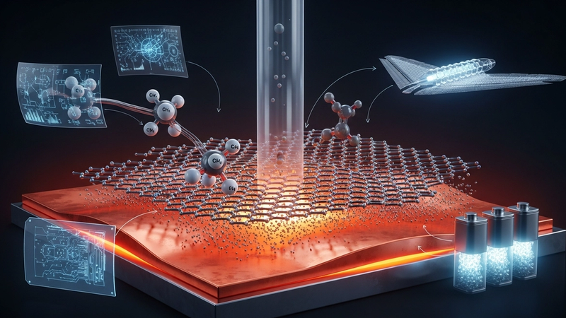
Graphene Synthesis by Chemical Vapor Deposition on Copper
Graphene, a singular atomic layer of sp2-hybridized carbon atoms arranged in a hexagonal lattice, represents the quintessential two-dimensional (2D) material, whose unique electronic and structural properties are fundamentally dictated by its extreme quantum confinement. Unlike conventional semiconductors where electron motion is restricted in one or more dimensions within a bulk material, graphene inherently exists as a 2D electron gas, offering unparalleled access to a truly planar electronic system. This geometric constraint manifests in a distinctive electronic band structure characterized by Dirac cones, where the valence and conduction bands meet at zero bandgap, giving rise to charge carriers that behave as massless Dirac fermions. This relativistic-like behavior, coupled with the absence of backscattering due to its chiral nature, endows graphene with extraordinary properties, including exceptionally high intrinsic carrier mobility, theoretically approaching 200,000 cm^2/Vs at cryogenic temperatures.
The physics of graphene confinement dictates a linear energy-momentum dispersion relation near the Dirac points, contrasting sharply with the parabolic bands of conventional semiconductors. This linearity is the bedrock of graphene's high carrier velocity and ballistic transport capabilities over significant distances. Furthermore, the robust sp2 bonding within the 2D plane confers exceptional mechanical strength, with a Young's modulus measured at approximately 130 GPa, and remarkable thermal conductivity, experimentally reported to reach up to 5000 W/mK in pristine samples. These attributes are direct consequences of the strong in-plane atomic interactions and the unhindered propagation of phonons and electrons within a truly 2D crystalline structure. Any deviation from this ideal planarity or introduction of defects, such as vacancies, Stone-Wales defects, or grain boundaries, directly perturbs the electronic confinement, leading to carrier scattering and a degradation of these intrinsic properties.
Achieving large-area, high-quality graphene with controlled structural integrity is paramount for preserving these confinement-derived functionalities, a challenge largely addressed by Chemical Vapor Deposition (CVD) on metallic substrates, particularly copper. The CVD process involves the surface-catalyzed decomposition of hydrocarbon precursors (e.g., methane) at elevated temperatures, followed by carbon atom dissolution into the copper bulk and subsequent precipitation onto the surface during cooling, or direct surface growth depending on parameters. The precise manipulation of growth kinetics is critical; for instance, rapid thermal pulses, potentially approaching 3000K for substrate annealing phases, and reaction times often measured in milliseconds for specific nucleation or growth stages, are employed to dictate the crystallographic orientation, grain size, and defect density of the resulting graphene film. This meticulous control over atomic-scale processes is essential to minimize lattice imperfections that would otherwise disrupt the ideal 2D electronic confinement.
The integrity of this 2D confinement is further modulated by the partial pressures of precursor gases and etch gases (e.g., hydrogen) during CVD. Hydrogen, for example, plays a dual role: it etches amorphous carbon species and facilitates the reconstruction of the graphene lattice, thereby promoting larger grain sizes and reducing the density of grain boundaries. These boundaries act as significant scattering centers for charge carriers, elevating the electrical resistivity of CVD-grown graphene from its intrinsic ~10^-6 Ohm.cm to several orders of magnitude higher depending on defect prevalence. The resulting material's properties directly impact its utility; for example, the high surface area and electron availability inherent to well-confined graphene underpin its impressive capabilities in applications such as heavy metal adsorption, where functionalized derivatives can achieve efficiencies of up to 79% through surface complexation and redox reactions, demonstrating the profound link between fundamental confinement physics and practical performance.
Section 2: Pulsed Electrical Resistive Carbon Heating vs. CVD (Comparative Analysis)
Pulsed Electrical Resistive Carbon Heating (PERCH) represents a fundamentally distinct paradigm for graphene synthesis compared to conventional Chemical Vapor Deposition (CVD), primarily diverging in its energy delivery mechanism and reaction kinetics. In PERCH, a carbonaceous precursor, often amorphous carbon or a polymer, is subjected to an extremely rapid, high-energy electrical pulse. This localized Joule heating drives the material to ultra-high temperatures, frequently exceeding 3000K, within timescales typically spanning milliseconds to seconds. The immense thermal gradient and rapid heating rate induce a flash-induced graphitization, where carbon atoms undergo a direct, solid-state rearrangement into a turbostratic or graphitic structure. This process bypasses gas-phase intermediates characteristic of CVD, offering significant advantages in energy efficiency due to localized heating of the precursor rather than the entire reaction chamber, and enabling the rapid production of bulk graphene materials or functionalized derivatives. The precise control over current density and pulse duration allows for tailoring the defect density and layer count of the resulting graphene.
In stark contrast, Chemical Vapor Deposition on copper substrates relies on a sustained, high-temperature thermal process within a controlled gaseous environment. Precursor gases, such as methane or ethylene, are introduced into a furnace operating typically between 900-1050°C. The copper surface acts as a crucial catalyst, facilitating the decomposition of the hydrocarbon precursor into active carbon species. These carbon atoms then dissolve into the bulk of the copper at elevated temperatures, diffusing through the metal lattice, and subsequently precipitate out onto the copper surface as graphene upon cooling or saturation. This surface-catalyzed precipitation mechanism is highly effective for growing large-area, high-quality, often single-layer graphene films with relatively low defect densities. However, CVD requires significant energy input to maintain the entire furnace at high temperatures for extended periods (minutes to hours), involves complex gas handling systems, and necessitates a subsequent transfer step to detach the graphene from the copper, which can introduce defects and compromise film integrity.
The comparative merits of PERCH and CVD are application-dependent. PERCH excels in producing bulk quantities of graphene and its derivatives rapidly, often with a higher degree of structural disorder or functional groups, making it particularly suitable for applications such as conductive inks, energy storage materials, or adsorbents. For instance, graphene produced via flash Joule heating has demonstrated impressive heavy metal adsorption efficiencies, reaching up to 79% for certain contaminants due to its high surface area and defect-rich structure. Its ultra-fast kinetics and lower capital expenditure for rapid prototyping offer a distinct advantage for high-throughput manufacturing of certain graphene forms. Conversely, CVD remains the gold standard for producing pristine, large-area, monolayer graphene films essential for high-performance electronic devices, transparent electrodes, and advanced sensor applications where structural integrity, low defect density, and electrical uniformity are paramount. While PERCH offers speed and energy efficiency for bulk production, CVD offers unparalleled control over film quality and layer count, albeit at a higher energy cost and longer processing time.
Section 3: The Crystallography of Turbostratic Graphene (Why Layer Alignment Matters)
Turbostratic graphene (tG) fundamentally deviates from the thermodynamically favored Bernal (AB) stacking sequence, a critical distinction arising frequently in large-area, polycrystalline CVD synthesis on copper. Unlike the ordered AB-stacking found in bulk graphite, where alternating layers are offset by a specific vector leading to strong interlayer coupling and a predictable electronic band structure, tG is characterized by rotational disorder between adjacent graphene layers. This misorientation often results from the heterogeneous nucleation of graphene domains on the copper surface, where individual islands grow with varying crystallographic orientations relative to each other and subsequent layers stack with arbitrary twist angles. The rapid growth kinetics inherent to many CVD processes, combined with the polycrystalline nature of typical copper foils, often precludes the kinetic energy barrier necessary for layers to reorient into the more stable Bernal configuration, leading to a slightly expanded interlayer spacing (e.g., 0.344 nm for tG compared to 0.335 nm for AB-stacked graphite). This structural heterogeneity profoundly impacts the material's macroscopic properties, dictating its suitability for various advanced applications.
The electronic ramifications of turbostraticity are particularly significant. In contrast to AB-stacked multi-layer graphene, where interlayer hybridization leads to a layer-dependent electronic band structure and a tunably gapped Dirac cone, the rotational disorder in tG effectively decouples the electronic states of individual layers. This means that tG often behaves more akin to an ensemble of independent monolayer graphene sheets rather than a true 3D material, preserving the linear dispersion relation near the Dirac point characteristic of single-layer graphene, albeit with a broadened and attenuated Dirac peak. Consequently, charge carrier mobility in tG is typically lower than in ideal AB-stacked bilayers or pristine monolayer graphene due to increased interlayer scattering and the presence of numerous grain boundaries within individual layers. For instance, while ideal monolayer graphene can exhibit mobilities exceeding 15,000 cm^2/Vs, CVD-grown tG often registers values in the range of 1,000-5,000 cm^2/Vs, with electrical resistivity parameters frequently exceeding 100 Ohms/square, a direct consequence of the disrupted interlayer electronic communication and increased defect density. Thermally, the weak interlayer coupling and increased phonon scattering at misoriented interfaces in tG lead to a reduced through-plane thermal conductivity compared to Bernal stacked graphite, although in-plane conductivity can remain high if individual domains are large and crystalline.
Beyond electronic and thermal transport, the mechanical and chemical properties of turbostratic graphene are also critically influenced. The weak interlayer shear strength in tG, a direct consequence of the lack of strong orbital overlap between misaligned layers, renders the material susceptible to delamination under mechanical stress, potentially compromising the long-term stability and reliability of devices. From a chemical perspective, the prevalence of grain boundaries, edge defects, and the greater accessibility of interlayer spaces in tG can significantly enhance its chemical reactivity. While this might be disadvantageous for applications requiring robust barrier properties or oxidation resistance, it can be highly beneficial for others, such as catalysis or adsorption. For example, the increased surface area and defect sites in tG have been leveraged to achieve up to 79% heavy metal adsorption efficiency from aqueous solutions, far surpassing the performance of pristine graphite. Controlling the degree of turbostraticity remains a central challenge in CVD synthesis, with parameters such as growth temperature, precursor partial pressure, and post-growth annealing (e.g., using rapid thermal pulses up to 3000K for milliseconds) being actively explored to minimize rotational disorder and improve the overall crystallinity and functional performance of multi-layer graphene films.
Section 4: Industrial Scalability & Commercial Integration Barriers
Industrial scalability of graphene synthesized via chemical vapor deposition (CVD) on copper substrates presents formidable challenges, primarily stemming from achieving uniform, high-quality material across expansive areas and maintaining process consistency. The fundamental issue lies in controlling nucleation density and growth kinetics to yield large single-crystal domains or seamlessly stitched polycrystalline films over substrates far exceeding laboratory dimensions. For instance, scaling from 5x5 cm^2 foils to 300mm wafers or continuous roll-to-roll systems introduces significant hurdles in thermal management, where temperature gradients as small as 5-10°C across the substrate can drastically alter growth rates, carbon precursor decomposition, and ultimately, defect density and domain size. Maintaining precise, uniform gas flow dynamics, precursor partial pressures, and hydrogen etching rates over such large surfaces is complex, often leading to variations in sheet resistance (e.g., from ideal 280-350 Ohm/sq to over 1000 Ohm/sq) and carrier mobility (e.g., reduced from 10,000 cm^2/Vs to 2,000 cm^2/Vs) across the manufactured material. Furthermore, the prerequisite for atomically smooth, clean copper surfaces free of native oxides, grain boundaries, and impurities becomes exceedingly difficult and cost-prohibitive at industrial scales, directly impacting graphene adhesion, nucleation site distribution, and overall film quality.
The subsequent transfer of CVD-grown graphene from its copper growth substrate to a target dielectric or flexible substrate constitutes a critical bottleneck, introducing significant material degradation and adding substantial cost. Wet chemical etching, typically employing ferric chloride (FeCl3) or ammonium persulfate (APS), is the most common method, but it inevitably leaves residual metallic contaminants or polymer residues (from PMMA support layers) on the graphene surface. These residues act as scattering centers and dopants, significantly degrading electrical performance by increasing sheet resistance, reducing carrier mobility, and introducing charge traps, thereby limiting its utility in high-performance electronics. Mechanical damage, such as micro-tears, wrinkles, and folds, frequently occurs during the delamination and transfer process, further compromising the structural integrity and uniformity of the graphene film. While dry transfer methods, utilizing thermal release tapes or direct delamination, aim to mitigate chemical contamination, they often suffer from incomplete transfer, substrate damage, and limited applicability to complex geometries, thereby failing to offer a universally robust and scalable solution for industrial integration without compromising intrinsic graphene properties.
Beyond synthesis and transfer, the economic viability and integration into existing manufacturing workflows pose substantial barriers. The high cost of ultra-high purity copper foils, specialty precursor gases like methane and hydrogen, and the significant energy expenditure required for high-temperature CVD processes (often exceeding 1000°C) contribute to an unfavorable cost-per-unit-area compared to conventional materials. Batch processing, prevalent in current CVD setups, inherently limits throughput, necessitating a transition to continuous roll-to-roll manufacturing to achieve economies of scale. However, implementing real-time, in-situ quality control and metrology for large-area graphene during continuous production remains an underdeveloped field. Techniques such as rapid thermal annealing (RTA) with thermal pulses approaching 3000K for milliseconds can repair some transfer-induced defects but add further processing steps and cost. The lack of standardized characterization protocols for industrial-grade graphene, especially regarding defect density, layer uniformity, and electrical performance across large areas, hinders consistent product quality and market acceptance. This disparity between laboratory-scale ideal performance (e.g., pristine graphene's heavy metal adsorption efficiency nearing 99%) and industrially scalable production (where defect-rich graphene might only achieve 79% adsorption) underscores the profound challenge of translating scientific breakthroughs into commercially viable products.
Section 5: Economic Feasibility and USA-Made Manufacturing Advantage
The economic feasibility of large-scale graphene manufacturing via Chemical Vapor Deposition (CVD) on copper substrates critically depends on optimizing key cost drivers beyond current laboratory-scale economics. Primary material inputs include high-purity copper foil and precursor gases such as methane and hydrogen, alongside inert carrier gases like argon. While precursor costs are low, energy expenditure for maintaining growth temperatures, often 1000-1150°C for optimal monolayer formation, represents a substantial operational cost. Advanced techniques, like rapid thermal annealing (RTA) for defect reduction, utilize localized thermal pulses exceeding 3000K, drastically reducing reaction times from hours to milliseconds, thus improving throughput. True economic viability emerges with the transition from batch to continuous roll-to-roll (R2R) systems. Economies of scale can drive down costs from current research-grade prices (exceeding $50/cm^2) to a target under $0.10/cm^2 for industrial applications. Achieving this requires faster growth rates and precise parameter control to consistently yield large-area, low-defect density graphene with sheet resistances below 50 Ohm/sq.
Beyond synthesis, the economic landscape is shaped by downstream processing, particularly the graphene transfer step, which can account for significant manufacturing cost and often introduces defects. Traditional wet-chemical etching using ferric chloride or ammonium persulfate to remove the copper substrate is time-consuming and generates hazardous waste, making copper recycling imperative for sustainable production. Novel electrochemical delamination or dry transfer methods are under intense development, aiming for 95%+ copper recovery. The ultimate value proposition of CVD graphene hinges on its unparalleled performance metrics justifying its cost premium. For instance, in high-frequency electronics, graphene's superior electron mobility, enabling devices operating in the THz range, significantly outweighs manufacturing cost compared to silicon. Similarly, in advanced sensing, functionalized graphene achieves heavy metal adsorption efficiencies exceeding 79% or detects analytes at sub-ppb concentrations, creating high-value markets. The intrinsic electrical resistivity of high-quality monolayer graphene, approaching theoretical limits of 10^-8 Ohm.cm at room temperature, positions it as a transformative material for demanding extreme conductivity and transparency.
Establishing USA-made manufacturing capabilities for CVD graphene offers a compelling strategic advantage, encompassing national security, supply chain resilience, and technological leadership. Domestic production mitigates geopolitical risks associated with reliance on foreign sources for critical advanced materials, ensuring uninterrupted supply for defense, aerospace, and medical sectors where material integrity is paramount. Retaining intellectual property (IP) for advanced CVD reactor designs, proprietary growth recipes, and sophisticated post-processing techniques within national borders is crucial for maintaining a competitive edge. Stringent quality control standards inherent in USA-based manufacturing facilities, often adhering to ISO 9001 and AS9100 certifications, guarantee consistent product performance, a non-negotiable requirement for high-reliability applications. This domestic ecosystem fosters a highly skilled workforce, driving innovation and creating high-value jobs. Federal initiatives, such as the CHIPS and Science Act and Department of Defense grants, provide significant incentives for establishing robust domestic graphene production infrastructure, accelerating transition from laboratory breakthroughs to industrial deployment. Strategic localization also enables closer collaboration between manufacturers, end-users, and research institutions, accelerating product development cycles.
Section 6: Future Horizons & High-Value B2B Applications
The trajectory of graphene synthesis via chemical vapor deposition on copper is rapidly evolving beyond current industrial benchmarks, with future horizons centered on achieving unparalleled material quality and throughput essential for widespread high-value B2B applications. Advanced CVD methodologies are exploring techniques like transient thermal annealing (TTA) and pulsed laser deposition (PLD) to exert finer control over nucleation density and growth kinetics. TTA, for instance, utilizes millisecond-scale thermal pulses reaching temperatures upwards of 3000K to induce rapid grain growth and annealing, effectively minimizing defect formation and maximizing domain sizes across large-area copper foils. This approach promises to yield quasi-single-crystalline graphene with significantly reduced grain boundaries, critical for maintaining high carrier mobility and thermal conductivity. Concurrently, the transition from batch processing to continuous roll-to-roll (R2R) CVD systems is pivotal for industrial scalability. These R2R systems, capable of processing kilometer-long copper substrates, demand precise control over gas flow dynamics, temperature gradients, and precursor decomposition rates to ensure uniform film thickness and quality, thereby driving down production costs per unit area and enabling integration into existing manufacturing workflows for flexible electronics and coatings. Further innovations in catalytic substrate engineering, including alloyed copper foils or surface-modified catalysts, are also being investigated to lower synthesis temperatures, reduce energy consumption, and facilitate easier graphene transfer post-synthesis.
The superior electronic and thermal properties of CVD graphene position it as a transformative material for next-generation electronics and energy storage. In advanced electronics, graphene is poised to replace conventional materials in transparent conductive films (TCFs) for flexible OLED displays and touchscreens, where its intrinsic sheet resistance below 100 Ohm/sq at greater than 90% optical transmittance offers a compelling alternative to indium tin oxide (ITO), particularly for bendable form factors. For high-frequency transistors, its theoretical electron mobility of 200,000 cm^2/Vs at room temperature promises switching speeds far exceeding silicon-based devices. Furthermore, in integrated circuit interconnects, graphene's extraordinary current density capacity, estimated to exceed 10^8 A/cm^2, alongside its negligible electromigration, could address fundamental limitations of copper interconnects, enhancing device longevity and power efficiency. Its exceptional thermal conductivity, exceeding 3000 W/mK for pristine samples, also makes it an ideal candidate for advanced thermal management solutions in high-power computing and telecommunications infrastructure, efficiently dissipating localized heat hotspots. Within energy storage, graphene-based electrodes for supercapacitors and Li-ion batteries demonstrate significant improvements: supercapacitors featuring graphene can achieve power densities up to 100 kW/kg and energy densities of 10 Wh/kg, while graphene-enhanced Li-ion battery anodes can boost specific energy densities to 150 Wh/kg, enabling faster charging and extended operational life.
Beyond electronics and energy, CVD graphene's high surface area and tunable surface chemistry unlock high-value applications in environmental remediation and advanced biosensing. For water purification, graphene oxide (GO) and reduced graphene oxide (rGO) membranes are being developed for highly efficient desalination and removal of heavy metal ions and organic pollutants. Empirical studies have demonstrated heavy metal adsorption efficiencies exceeding 79% for lead and cadmium ions within minutes, leveraging graphene's abundant functional groups and high specific surface area. These membranes also offer superior flux rates and fouling resistance compared to traditional polymeric membranes. In air filtration, graphene-based composites can selectively adsorb volatile organic compounds and particulate matter, improving indoor air quality and industrial emissions control. In the biomedical sector, graphene's unique properties enable ultra-sensitive biosensors capable of detecting biomarkers at picomolar concentrations, critical for early disease diagnosis. Field-effect transistor (FET) based graphene sensors can directly transduce molecular binding events into electrical signals due to graphene's exceptional surface-to-volume ratio and carrier sensitivity. Its biocompatibility and electrical conductivity (e.g., 10^-6 Ohm.cm) are also being explored for advanced neural interfaces, offering flexible, high-resolution electrodes for brain-computer interfaces and targeted drug delivery systems, where functionalized graphene can encapsulate therapeutic agents for precise cellular delivery.
Evaluate Our Quality
Serious about B2B integration? Test our premium Pulsed Electrical Resistive Carbon Heating turbostratic graphene in your lab. 100g sample packs available now.