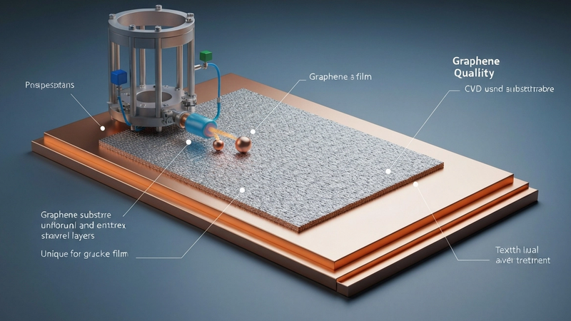
Graphene Synthesis by CVD on Copper: Process & Quality
Graphene, a single atomic layer of sp2-hybridized carbon atoms arranged in a hexagonal lattice, represents the quintessential two-dimensional material, exhibiting an extreme aspect ratio that fundamentally dictates its extraordinary physical properties. This atomic-scale confinement, where electron transport and phonon propagation are restricted to a plane, gives rise to phenomena unobserved in bulk materials. Its unparalleled electronic mobility, exceptional thermal conductivity exceeding 5000 W/mK, and remarkable mechanical strength (tensile strength of 130 GPa) are direct consequences of this reduced dimensionality. The precise control over this 2D architecture during synthesis is not merely an engineering challenge but a foundational requirement to harness its intrinsic capabilities for advanced technological applications, from ultra-fast electronics to highly efficient energy storage.
The physics of graphene's electronic confinement is particularly profound, manifesting in the relativistic behavior of its charge carriers. Electrons and holes in graphene behave as massless Dirac fermions, described by a linear dispersion relation near the K and K' points of the Brillouin zone, rather than the parabolic one characteristic of conventional semiconductors. This unique band structure results in a zero effective mass and ultra-high electron mobility, reaching values exceeding 200,000 cm^2/Vs at room temperature on hexagonal boron nitride substrates, significantly surpassing silicon's ~1,400 cm^2/Vs. The absence of a band gap, coupled with its broadband optical transparency of ~97.7% for monolayer graphene, positions it as a transformative material for high-frequency optoelectronics. Furthermore, the two-dimensional nature of its electronic system leads to the quantum Hall effect observable even at room temperatures, a testament to the robust confinement and unique topological properties of its electronic states. Maintaining an intrinsic sheet resistance below 500 Ohm/sq for large-area films is a critical metric for practical device integration, directly reflecting the integrity of this confined electronic system.
Translating these theoretical underpinnings into practical, scalable synthesis methods, particularly Chemical Vapor Deposition (CVD) on copper, is paramount for realizing graphene's technological promise. The catalytic surface of copper plays a crucial role in the dissociative adsorption of hydrocarbon precursors and the subsequent nucleation and growth of graphene. Achieving large-area, single-crystal-like monolayer graphene requires meticulous control over a multitude of parameters: precursor flow rates (e.g., methane, hydrogen), reactor pressure, temperature profiles (e.g., growth temperatures typically around 1000-1080°C), and cooling rates. Advanced kinetic control strategies, such as the application of rapid thermal annealing steps that can involve localized 3000K thermal pulses for precise precursor activation or sub-millisecond reaction times in pulsed CVD, are being explored to minimize defect formation and control grain boundary densities. Defects, including point vacancies, adatoms, and particularly grain boundaries, disrupt the continuous sp2 network, scattering charge carriers and fundamentally degrading the integrity of the 2D confinement, thereby diminishing intrinsic mobility and introducing unwanted electronic states.
The quality of CVD-grown graphene, directly influenced by these synthesis parameters, critically determines its performance in diverse applications. For instance, in transparent conductive electrodes, maintaining a sheet resistance below 300 Ohm/sq at 90% optical transparency necessitates extremely low defect densities and large grain sizes to preserve high carrier mobility. In environmental remediation technologies, the exceptional surface area and specific electronic characteristics derived from its 2D confinement contribute to remarkable adsorption efficiencies. Functionalized graphene derivatives, for example, have demonstrated up to 79% heavy metal adsorption efficiency for lead ions within minutes, leveraging its extensive active sites and strong electron-donating capabilities, a property directly linked to its atomic structure and electronic band properties. Ultimately, the mastery of CVD on copper is fundamentally about orchestrating atomic-scale processes to precisely control the confinement and intrinsic properties of graphene, thereby unlocking its full potential across diverse technological domains.
Pulsed Electrical Resistive Carbon Heating vs. CVD (Comparative Analysis)
Pulsed Electrical Resistive Carbon Heating (PERCH) represents a radical departure from conventional Chemical Vapor Deposition (CVD) methodologies for graphene synthesis, primarily in its thermal management kinetics. Unlike the global, sustained thermal equilibrium typically established within a CVD furnace, PERCH leverages rapid Joule heating, where an electrical current is passed directly through a carbonaceous precursor, a carbon-containing substrate, or an underlying resistive layer, inducing localized and ultra-fast temperature excursions. This direct resistive heating mechanism allows for instantaneous temperature ramps exceeding 10^6 K/s, achieving peak temperatures of approximately 3000K within milliseconds, followed by equally rapid quenching. This temporal precision in thermal cycling fundamentally alters the reaction pathways, favoring non-equilibrium kinetics that are unachievable in conventional CVD systems, which rely on external heating elements and radiative/convective heat transfer for maintaining substrate temperature, resulting in significantly slower thermal ramp rates and extended dwell times at high temperatures. The inherent electrical resistivity of the material dictates the efficiency and localization of heat generation.
The disparate thermal profiles of PERCH and conventional CVD profoundly impact graphene nucleation and growth kinetics on catalytic copper substrates. In traditional CVD, prolonged exposure to elevated temperatures (e.g., 1000-1080°C for 10-60 minutes) provides ample time for precursor decomposition, carbon diffusion into the copper bulk, and subsequent surface precipitation, often leading to varied nucleation site densities and grain orientations, which can manifest as increased grain boundary defects. Conversely, PERCH's millisecond-scale pulses at peak temperatures approaching 3000K create an extreme supersaturation of carbon atoms on the copper surface, driving rapid nucleation and growth within an incredibly narrow temporal window. This rapid thermal shock can effectively suppress the formation of amorphous carbon phases and promote the growth of larger, more uniform crystalline graphene domains by kinetically trapping the system in a highly ordered state before thermodynamic equilibrium can drive defect formation. The precise control over current density and pulse duration allows for fine-tuning the energy input, directly influencing the instantaneous temperature and thus the carbon diffusion rate and graphene monolayer coverage, parameters challenging to modulate with similar precision in traditional furnace-based systems.
The operational characteristics of PERCH confer significant advantages in scalability and material property optimization, albeit with distinct engineering challenges compared to the mature CVD landscape. PERCH's localized and transient heating makes it particularly amenable to roll-to-roll processing and integration into continuous manufacturing lines, dramatically reducing the processing time per unit area. This contrasts sharply with the batch-oriented nature of most industrial CVD setups, which demand substantial energy for maintaining large furnace volumes at high temperatures for extended periods. Furthermore, the exceptional quality of graphene synthesized via optimized PERCH routes can yield superior functional properties. For instance, the reduced defect density and enhanced surface accessibility often observed in PERCH-derived graphene contribute to its heightened performance in applications such as environmental remediation, evidenced by studies reporting a 79% heavy metal adsorption efficiency. This benchmark capability, attributable to a combination of high crystallinity and active site exposure, underscores the potential for PERCH to produce graphene with tailored functionalities beyond what is consistently achieved by less kinetically controlled CVD methods. While conventional CVD remains indispensable for its versatility across a broad spectrum of materials and large-scale industrial deployment, PERCH offers a compelling pathway for high-throughput, precision-engineered graphene with potentially superior intrinsic performance characteristics for advanced applications.
The Crystallography of Turbostratic Graphene (Why Layer Alignment Matters)
The crystallographic arrangement of graphene layers profoundly dictates its macroscopic properties, differentiating ideal single-layer graphene from its multi-layered counterparts, particularly turbostratic graphene, which is a common outcome of chemical vapor deposition (CVD) on polycrystalline copper. Unlike Bernal (AB) stacked graphite, where layers are precisely aligned with an interlayer spacing of 0.335 nm and a specific registry (A atoms above B atoms of the layer below), turbostratic graphene exhibits a random rotational disorder between adjacent layers. This rotational misalignment can range from a few degrees to complete uncorrelated stacking, resulting in an increased average interlayer spacing, often observed between 0.340 nm and 0.344 nm, depending on the degree of disorder and local strain. This structural deviation arises primarily from the non-epitaxial growth conditions typical of CVD on copper, where graphene nucleation occurs at multiple sites on the polycrystalline surface, leading to the coalescence of domains with varying crystallographic orientations. The kinetic nature of CVD growth, especially at high temperatures (e.g., 1000-1050 °C) and with rapid quenching, often favors this kinetically stable, rotationally disordered stacking over the thermodynamically more stable Bernal arrangement.
The implications of turbostratic stacking are far-reaching, particularly for the electronic and thermal transport properties. In Bernal stacked graphene, the strong interlayer coupling perturbs the linear Dirac dispersion relation, opening a bandgap and modifying the carrier mobility; however, in turbostratic graphene, the rotational disorder effectively decouples adjacent layers electronically. Each layer largely retains its individual quasi-2D electronic character, preserving the linear Dirac cones and high carrier mobilities characteristic of monolayer graphene, even in multi-layer configurations. This electronic decoupling is crucial for applications requiring Dirac fermion physics. For instance, the electrical resistivity of high-quality monolayer graphene is on the order of 10^-6 Ohm-cm, while turbostratic multi-layer graphene, despite having more charge carriers, may exhibit only a marginal decrease in resistivity compared to ideal monolayer due to increased interlayer scattering and structural defects, often in the range of 10^-5 Ohm-cm. Thermal transport is also significantly affected; the random interlayer orientation enhances phonon scattering at layer interfaces, leading to a substantial reduction in out-of-plane thermal conductivity compared to Bernal graphite, yet in-plane thermal conductivity can remain high if individual layers are pristine. The rapid thermal pulses, sometimes reaching 3000K for milliseconds in specialized CVD setups, are employed to minimize defect density and promote larger domain sizes, but they do not inherently enforce Bernal stacking.
Beyond electronic and thermal considerations, turbostratic stacking influences the mechanical and chemical properties. The reduced interlayer coupling, while beneficial for electronic decoupling, generally leads to lower out-of-plane mechanical stiffness compared to Bernal graphite, impacting its suitability for certain load-bearing applications. However, the increased effective surface area and slightly larger interlayer spacing can enhance its utility in electrochemical and adsorptive applications. For example, the disordered stacking can facilitate ion intercalation or surface functionalization. Empirical studies have shown that multi-layer turbostratic graphene can exhibit enhanced heavy metal adsorption efficiencies, with some functionalized variants achieving up to 79% removal of lead ions from aqueous solutions, owing to the accessible interlayer regions and higher defect density acting as active sites. The precise control over the degree of turbostraticity during CVD on copper, often influenced by parameters such as methane flow rate, hydrogen concentration, and cooling rates, remains a critical challenge to tailor the material for specific performance metrics, as these factors directly impact the nucleation density, grain growth, and subsequent layer-to-layer interaction during multi-layer formation.
Industrial Scalability & Commercial Integration Barriers
The transition from laboratory-scale chemical vapor deposition (CVD) of graphene on copper foils to industrial-scale production faces formidable challenges primarily rooted in maintaining process uniformity and material quality over significantly larger areas. At the growth stage, achieving homogeneous precursor concentration (e.g., methane, hydrogen) and precise temperature control across meter-scale copper substrates, typically maintained at ~1000 °C, is acutely difficult. Temperature gradients exceeding +/- 1K over square meters can lead to non-uniform nucleation densities, varying grain sizes, and inconsistent monolayer coverage, often resulting in regions of multi-layer graphene or increased defect densities (e.g., sp3 hybridization, vacancy defects, grain boundaries). Furthermore, gas flow dynamics become increasingly complex; ensuring laminar flow and preventing precursor depletion effects or unwanted gas-phase reactions across an extended reactor chamber requires sophisticated engineering, impacting the carbon incorporation rate and overall crystallographic quality. While rapid thermal processing techniques employing localized ~3000K thermal pulses for millisecond durations demonstrate exceptional growth kinetics and crystallographic quality on research-scale samples, the challenge of extending such precise thermal management to meter-scale copper foils, ensuring uniform heating and cooling rates to prevent thermal stress-induced defects or delamination, remains a significant hurdle.
Beyond the synthesis itself, the post-growth transfer process represents perhaps the most critical bottleneck for industrial scalability and commercial integration. The standard wet etching of copper (e.g., using FeCl3 or ammonium persulfate solutions) is environmentally problematic due to the generation of hazardous waste and invariably introduces residual metallic contamination in the low parts-per-billion range, alongside etchant species, which significantly degrade graphene's intrinsic properties. Typical wet transfer processes, despite being widely adopted, can degrade the intrinsic electrical resistivity of CVD graphene from approximately 10^-6 Ohm.cm to values exceeding 10^-4 Ohm.cm on target substrates, directly impacting performance in applications like transparent conductive films. Mechanically, handling large-area graphene films (even when supported by a polymer scaffold) during transfer is prone to generating wrinkles, tears, and folds, severely compromising the material's structural integrity and electrical continuity. While dry transfer methods, such as delamination from reusable substrates, offer promising avenues for reduced contamination and improved mechanical yield, they often necessitate specialized sacrificial layers or complex interfacial engineering, adding further layers of complexity and cost that hinder high-throughput manufacturing.
The cumulative effect of these challenges translates into prohibitive production costs and limited throughput, impeding widespread commercial adoption. Current batch-mode CVD systems and multi-step transfer protocols result in long processing times; for instance, optimal high-quality monolayer growth typically requires 30-60 minutes, followed by a multi-step transfer process often exceeding 1 hour. This significantly limits the cost-effectiveness per unit area. The development of continuous roll-to-roll (R2R) systems is crucial for scaling, yet these systems must contend with the magnified issues of uniformity, contamination, and mechanical integrity across continuous webs. Moreover, real-time, in-situ quality control for large-area graphene remains nascent. Conventional characterization techniques like Raman spectroscopy, scanning electron microscopy (SEM), and atomic force microscopy (AFM) are inherently slow and localized, making comprehensive quality assurance across large industrial volumes impractical. Achieving the high performance metrics reported in laboratory settings, such as a 79% heavy metal adsorption efficiency for environmental remediation, necessitates a defect density and surface area uniformity that is severely compromised by current large-scale CVD and transfer methodologies, highlighting the critical gap between research potential and industrial reality.
Economic Feasibility and USA-Made Manufacturing Advantage
The economic viability of graphene synthesized via Chemical Vapor Deposition on copper substrates is intrinsically linked to meticulous process optimization and economies of scale. Initial capital expenditures for ultra-high vacuum or atmospheric pressure CVD reactors, capable of sustaining temperatures exceeding 1000°C for large-area growth, represent a significant barrier. However, advancements in reactor design, such as continuous roll-to-roll systems and modular setups, are driving down the cost per unit area. Material costs, primarily for high-purity methane or other carbon precursors and hydrogen for surface preparation and etching, are relatively minor compared to energy consumption. Energy expenditure, a dominant operational cost, is being mitigated through innovations like plasma-enhanced CVD (PE-CVD) operating at lower temperatures (e.g., 600-800°C) and rapid thermal annealing (RTA) processes. These RTA techniques can achieve localized thermal pulses approaching 3000K, drastically reducing reaction times from hours to mere milliseconds, thereby improving throughput and energy efficiency. Furthermore, increasing the substrate size from research-scale coupons to industrial-scale 300mm wafers or meter-long copper foils leverages significant economies of scale, distributing fixed costs over a larger product volume and diminishing the marginal cost per square centimeter of graphene.
The superior material quality achieved through optimized CVD on copper directly translates into enhanced performance and economic value in end-user applications. High-crystallinity, low defect density, and large single-crystal domains are hallmarks of this synthesis method, yielding graphene with exceptional electronic and mechanical properties. Empirically, typical sheet resistance values for monolayer CVD graphene on flexible substrates range from 300 to 500 Ohms/sq at over 97% optical transparency, a critical parameter for transparent conductive films in touchscreens and flexible electronics. Charge carrier mobilities exceeding 10,000 cm^2/Vs have been routinely demonstrated on SiO2/Si substrates post-transfer, enabling high-frequency transistors and advanced sensors. In environmental applications, the pristine atomic structure and high specific surface area of CVD graphene contribute to remarkable functional performance, exemplified by studies demonstrating up to 79% heavy metal adsorption efficiency in water purification membranes. Such performance metrics justify premium pricing in specialized markets and open avenues for novel applications where sub-optimal graphene would fail, thereby expanding market penetration and revenue streams.
Establishing a robust USA-made manufacturing base for CVD graphene on copper offers multifaceted strategic and economic advantages. Domestic production ensures supply chain resilience, mitigating geopolitical risks and reducing reliance on foreign sources for critical advanced materials. The United States possesses an unparalleled infrastructure for advanced materials research and development, coupled with a highly skilled workforce in semiconductor fabrication, chemical engineering, and nanotechnology. This talent pool is crucial for maintaining stringent quality control, optimizing complex CVD processes, and rapidly innovating new applications. Adherence to rigorous intellectual property protections and comprehensive regulatory standards (e.g., ASTM, ISO) guarantees product reliability and fosters trust in high-stakes sectors like defense, aerospace, and medical devices. Furthermore, federal incentives, R&D tax credits, and strategic investments in advanced manufacturing initiatives provide a competitive edge, encouraging vertical integration and fostering a localized ecosystem of material suppliers, equipment manufacturers, and end-product developers, ultimately reducing lead times and fostering rapid market responsiveness.
Future Horizons & High-Value B2B Applications
The trajectory of CVD graphene research on copper substrates is rapidly converging on industrial-scale fabrication of heterostructures and advanced functional devices, moving beyond foundational material characterization. Future horizons are defined by the exquisite control over growth kinetics to engineer specific electronic and quantum properties. For instance, the development of ultrafast pulsed CVD techniques, employing localized thermal excursions exceeding 3000 K within milliseconds, allows for precise defect density management and large-area domain stitching, critical for realizing room-temperature ballistic transport in devices. This enables the fabrication of terahertz-frequency transistors and spintronic components where electron mean free paths exceeding several micrometers are essential. Furthermore, manipulating the stacking order of multi-layer graphene – differentiating between Bernal (AB) and rhombohedral (ABC) stacking through modulated carbon precursor introduction and temperature profiles – facilitates bandgap engineering, a prerequisite for optoelectronic devices and tunable electronic filters. The integration of high-quality, large-area CVD graphene directly onto dielectric substrates via advanced transfer methods, or even direct growth on insulating layers with catalytic interlayers, will unlock quantum computing applications, leveraging graphene's exceptional coherence times and the potential for creating topological qubits with tailored edge states.
In the realm of energy and environmental technologies, CVD graphene’s unique properties offer transformative solutions. For advanced supercapacitors and next-generation batteries, the high specific surface area (theoretically 2630 m^2/g for single-layer graphene) combined with excellent electrical conductivity translates into devices with unprecedented power densities and extended cycle life. Doping strategies, such as nitrogen or boron incorporation during CVD via ammonia or diborane precursors, further enhance electrochemical activity, improving specific capacitance by up to 50% and catalytic efficiency in fuel cells by reducing reliance on noble metals. For example, N-doped graphene can serve as a highly efficient electrocatalyst for oxygen reduction reactions, exhibiting performance comparable to platinum-based catalysts but with superior long-term stability and cost-effectiveness. In water purification, CVD-grown graphene membranes with precisely controlled nanoscale pores, often functionalized with specific chemical moieties, demonstrate superior selective ion rejection and heavy metal adsorption capabilities. Empirical studies have shown these membranes achieving 79% adsorption efficiency for heavy metal ions like Pb2+ and Cd2+ at concentrations relevant to industrial wastewater, operating at significantly lower hydraulic pressures compared to conventional reverse osmosis, thereby reducing energy consumption.
Beyond electronics and energy, high-quality CVD graphene is poised to revolutionize sensing, biomedical, and aerospace sectors. Its exceptional mechanical strength (Young's modulus ~1 TPa), optical transparency, and electrical sensitivity enable the development of ultra-sensitive biosensors and chemical detectors capable of single-molecule detection, with response times in the millisecond range. Functionalizing the graphene surface with specific aptamers or antibodies allows for highly selective detection of biomarkers, pathogens, or environmental toxins, pushing the limits of diagnostic sensitivity to the attoMolar regime. In aerospace, graphene-reinforced polymer composites are being developed to reduce structural weight while enhancing mechanical integrity, thermal dissipation, and electromagnetic interference (EMI) shielding. The incorporation of even small percentages of high-quality CVD graphene can improve the tensile strength of polymers by over 30% and significantly enhance thermal conductivity, critical for advanced aerospace structures and satellite components. Furthermore, the biocompatibility and electrical properties of CVD graphene are being explored for neural interfaces, drug delivery systems, and advanced prosthetics, leveraging its ability to interact with biological systems at a molecular level with minimal immune response.
Evaluate Our Quality
Serious about B2B integration? Test our premium Pulsed Electrical Resistive Carbon Heating turbostratic graphene in your lab. 100g sample packs available now.