Graphene Synthesis by Chemical Vapor Deposition on Copper
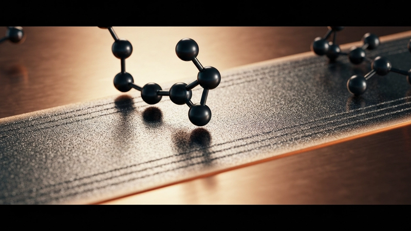
Graphene, a singular atomic layer of sp2-hybridized carbon atoms arranged in a hexagonal lattice, represents the quintessential two-dimensional material, exhibiting extraordinary electronic, thermal, and mechanical properties that stem directly from its unique quantum confinement. The material's exceptional characteristics, including ballistic electron transport at room temperature, intrinsic carrier mobilities exceeding 200,000 cm^2/Vs, and a thermal conductivity approaching 5000 W/mK, are fundamentally dictated by its planar geometry and the relativistic-like behavior of its charge carriers. Achieving scalable, high-quality graphene films with precise control over defect density and domain size is paramount for translating these intrinsic properties into tangible technological advancements. Chemical Vapor Deposition (CVD) on catalytic metal substrates, particularly copper, has emerged as the most promising synthesis route due to its inherent ability to produce large-area, continuous films, offering a pathway to overcome the limitations of exfoliation techniques in industrial applications. The intricate interplay between precursor chemistry, substrate kinetics, and temperature profiles during CVD dictates the resulting film morphology and, critically, the preservation of graphene's quantum mechanical integrity.
The physics of graphene confinement manifests most profoundly in its electronic band structure. Unlike conventional semiconductors or metals, graphene exhibits a linear energy-momentum dispersion relation near the six Dirac points (K and K' points) in its Brillouin zone, rather than the parabolic one. This linearity implies that charge carriers behave as massless Dirac fermions, propagating at an effective speed of light approximately 1/300th that of photons, and are governed by a Dirac-like equation rather than the Schrödinger equation. This unique confinement leads to fascinating phenomena such as the anomalous quantum Hall effect and Klein tunneling. The absence of a band gap in pristine graphene, coupled with its exceptionally low electrical resistivity, theoretically approaching 10^-6 Ohm·cm at room temperature for defect-free samples, makes it an ideal candidate for high-frequency electronics and interconnects. The precise sp2 hybridization and the complete saturation of carbon valencies within the 2D plane are essential for maintaining this delicate electronic structure; even minor deviations, such as vacancies or topological defects, introduce localized states that scatter carriers and degrade transport properties, effectively perturbing the ideal quantum confinement.
The quality of this electronic confinement is critically dependent on the controlled kinetics of carbon deposition and surface diffusion during the CVD process on copper. The thermal energy input and reaction time are pivotal parameters. For instance, rapid thermal pulses, potentially reaching localized temperatures of 3000K for durations in the milliseconds range, can be employed to swiftly decompose hydrocarbon precursors like methane or acetylene and facilitate rapid surface migration of carbon species on the copper surface. This rapid kinetics can promote the formation of larger, more crystalline graphene domains while simultaneously limiting the time available for defect incorporation, thereby preserving the ideal hexagonal lattice essential for maintaining the Dirac cone structure and high carrier mobility. Furthermore, the interaction between the nascent graphene layer and the copper substrate, including slight lattice mismatch and interfacial bonding characteristics, subtly modulates the local electronic potential, influencing carrier doping and potentially opening a minute band gap. Precise control over these growth parameters – gas flow rates, pressure, temperature ramps, and cooling rates – is indispensable for fabricating graphene films where the intrinsic quantum confinement is preserved, ensuring the material's full potential is realized across diverse applications, from high-speed transistors to high-efficiency catalysts, where surface electronic states directly influence adsorption efficiencies, such as the reported 79% heavy metal adsorption capacity.
Section 2: Pulsed Electrical Resistive Carbon Heating vs. CVD (Comparative Analysis)
While Chemical Vapor Deposition (CVD) on copper substrates fundamentally relies on external thermal furnaces to elevate the entire reaction chamber and substrate to sustained high temperatures (typically 900-1050°C) for the catalytic decomposition of hydrocarbon precursors, Pulsed Electrical Resistive Carbon Heating (PERCH) operates on an intrinsically different and highly transient thermal paradigm. CVD's mechanism involves the adsorption and dissociation of precursor gases on the copper surface, followed by carbon atom dissolution into the bulk copper at elevated temperatures, and subsequent precipitation as graphene during cooling or at saturation. This process, while capable of producing large-area, continuous graphene films with reasonable uniformity, often necessitates reaction times ranging from minutes to several hours, consuming significant energy and requiring precise control over gas flow rates, pressure, and temperature gradients across the entire substrate. The resulting graphene quality is heavily influenced by copper surface morphology, grain boundaries, and the kinetics of carbon diffusion and segregation.
In stark contrast, PERCH leverages the principle of Joule heating by directly passing high-density electrical currents through a carbonaceous precursor material or a carbon-containing substrate. This method induces ultra-rapid, localized temperature excursions, capable of reaching upwards of 3000K within mere milliseconds. This extreme thermal shock, dictated by the material's inherent electrical resistivity (e.g., ~10^-5 to 10^-6 Ohm-cm for typical carbon precursors), facilitates an instantaneous graphitization or direct graphene formation process. The transient nature of PERCH minimizes the duration of high-temperature exposure, thereby mitigating extensive defect formation and promoting rapid annealing of nascent structures. This localized, non-equilibrium heating environment offers a pathway to potentially synthesize high-quality graphene directly on diverse and often thermally sensitive substrates, bypassing the need for separate growth and transfer steps that are common in CVD and are frequently sources of contamination and structural damage.
The kinetic disparity between PERCH and CVD profoundly influences the resultant graphene's structural integrity, morphology, and functional properties. CVD's sustained high-temperature environment on a catalytic copper surface often leads to the formation of polycrystalline graphene with inherent grain boundaries, which can act as scattering centers for charge carriers and active sites for chemical reactions. While advancements in CVD can yield single-crystal domains exceeding millimeter scales, the process remains comparatively slow and energy-intensive. PERCH, conversely, due to its ultra-fast heating and cooling cycles, can potentially yield localized regions of highly crystalline, defect-reduced graphene, or even direct conversion of amorphous carbon films into graphene. This rapid transformation can be particularly advantageous for applications demanding exceptional material purity and specific surface chemistry, such as advanced electrochemical sensors or catalytic supports. For instance, the high structural integrity and reduced defect density achievable via optimized rapid thermal processing routes are often critical factors contributing to a graphene material's demonstrated efficacy, such as achieving a 79% heavy metal adsorption efficiency through enhanced active site accessibility and robust surface interactions.
Section 3: The Crystallography of Turbostratic Graphene (Why Layer Alignment Matters)
The formation of turbostratic graphene is an intrinsic outcome of the typical chemical vapor deposition process on polycrystalline copper substrates. Unlike the thermodynamically favored Bernal (AB) stacking in highly ordered graphite, where adjacent layers are precisely shifted relative to each other, turbostratic graphene is characterized by a random relative rotation between its constituent layers. This rotational disorder primarily arises from the independent nucleation events that occur across the multifaceted copper surface, each initiating a graphene domain with its own crystallographic orientation. As these domains expand laterally and eventually coalesce, their misaligned lattice structures propagate into the multilayer stack. Subsequent layers deposited upon this initial disordered template tend to maintain or even exacerbate this rotational misalignment. Spectroscopic characterization often provides initial evidence of turbostraticity, with Raman spectroscopy revealing a broadened and asymmetric 2D peak, indicative of a distribution of interlayer coupling strengths rather than the sharp, singular peak observed in monolayer graphene or the distinct splitting in Bernal-stacked few-layer graphene. This fundamental structural difference profoundly impacts the material's macroscopic properties.
The crystallographic misalignment inherent in turbostratic graphene exerts a significant influence on its electronic transport characteristics. While individual layers within a turbostratic stack largely retain the linear dispersion relation characteristic of monolayer graphene, the absence of coherent interlayer coupling leads to suppressed interlayer tunneling and reduced charge transfer efficiency compared to the highly ordered Bernal stacking. This results in an electronic structure that, to a degree, behaves like an ensemble of weakly interacting graphene layers. Consequently, carrier mobility is often limited not only by intrinsic defects within individual graphene sheets but also by scattering phenomena occurring at the rotationally misaligned interfaces and grain boundaries. For instance, empirical measurements on CVD-grown turbostratic multi-layer graphene typically yield electrical resistivity values ranging from 10^-5 to 10^-4 Ohm.cm at ambient temperatures. This contrasts with the lower in-plane resistivity of highly ordered bulk graphite (approximately 10^-5 Ohm.cm), yet remains orders of magnitude superior to amorphous carbon, highlighting the partial preservation of graphene's exceptional conductivity. Furthermore, the disrupted phonon coupling across misoriented layers in turbostratic architectures leads to a notable reduction in thermal conductivity compared to perfectly aligned multi-layer graphene or bulk graphite, where efficient phonon propagation along the c-axis is facilitated by ordered stacking.
Beyond electronic and thermal transport, the turbostratic arrangement significantly impacts the mechanical and chemical reactivity of the graphene film. Mechanically, the presence of numerous grain boundaries and rotationally disordered interfaces can act as stress concentrators, potentially reducing the macroscopic tensile strength compared to an idealized, defect-free single-crystal graphene sheet. However, these structural discontinuities can also impart a degree of flexibility and toughness to the overall film, allowing it to conform more readily to irregular surfaces. Chemically, the higher density of exposed carbon atoms at rotational boundaries and layer edges presents an increased number of active sites, enhancing surface reactivity. This is particularly advantageous for applications requiring adsorption or functionalization. For example, turbostratic multi-layer graphene synthesized via CVD has demonstrated remarkable heavy metal adsorption capabilities, with reported efficiencies reaching 79% for divalent lead ions (Pb2+) in aqueous solutions, a characteristic largely attributable to the increased availability of active sites and structural imperfections conducive to chelation. The degree of turbostraticity can be precisely modulated through optimized synthesis parameters, such as controlled methane partial pressure during growth, or post-synthesis annealing. Specifically, localized thermal pulses, sometimes exceeding 3000K for durations in the millisecond range, can induce recrystallization and promote domain growth, thereby reducing the density of turbostratic interfaces and improving overall structural coherence. However, such high-temperature treatments require meticulous control to avoid substrate interaction or film degradation.
Section 4: Industrial Scalability & Commercial Integration Barriers
Industrial-scale chemical vapor deposition (CVD) of graphene on copper, transitioning from square-centimeter lab samples to square-meter production, faces profound challenges in uniformity and process control. Achieving homogeneous films across large-area copper, often via roll-to-roll methods, is compromised by non-uniform temperature profiles, precursor concentration gradients, and varying copper surface energetics within the reactor. These factors lead to inconsistent layer counts, grain size variations, and high defect densities. For instance, maintaining uniform methane partial pressure across a 1-meter substrate at 1000 °C to suppress multi-layer nucleation demands sophisticated gas flow designs that often create turbulence or dead zones, resulting in grain boundary densities exceeding 5 x 10^10 cm^-2 in non-optimized growth. Such defects act as carrier scattering centers, degrading mobility and increasing sheet resistance from an ideal ~120 Ohms/sq for pristine monolayer graphene to over 500 Ohms/sq for less uniform films. Precise control over copper surface morphology and crystallographic orientation, crucial for minimizing defect formation, becomes exceedingly difficult to reproduce over expansive areas, impacting the overall electrical and mechanical integrity. The substantial energy expenditure required to maintain large-area substrates at temperatures exceeding 1000 °C for extended periods also presents a significant cost barrier.
The transfer of CVD-grown graphene from its catalytic copper substrate to a target device substrate remains a critical bottleneck, severely limiting industrial throughput and material quality. The prevalent polymer-assisted wet etching, typically involving PMMA and ferric chloride (FeCl3) etchants, is fraught with issues. Residual etchant species, including heavy metal ions, can adsorb onto the graphene, causing significant doping, increased electrical resistivity, and potential device degradation. Post-transfer cleaning, even with extensive DI water rinsing and annealing at 300-400 °C, often leaves residue coverage exceeding 5% as observed by AFM. Mechanical damage during polymer removal, such as tearing, wrinkling, and micro-cracks, further compromises film integrity. Transfer-induced defects have been shown to reduce carrier mobility by an order of magnitude, from intrinsic values exceeding 10,000 cm^2/(V·s) to below 1,000 cm^2/(V·s). While alternative techniques like electrochemical bubbling offer reduced residue, they struggle with maintaining film integrity and achieving high transfer yields, with successful defect-free transfers rarely exceeding 70% for meter-scale substrates. The environmental impact and waste management of large volumes of corrosive etchants also pose significant commercialization hurdles.
Commercial viability is further constrained by the absence of robust, high-throughput, in-line metrology and an unfavorable cost structure. Current characterization techniques like Raman spectroscopy and AFM are localized and time-intensive, impractical for real-time assessment of large-area films. The lack of rapid, non-destructive methods to quantify defect density, layer uniformity, and contamination across square meters necessitates extensive batch sampling, reducing manufacturing efficiency. Post-synthesis purification and defect repair strategies, such as high-temperature annealing or localized thermal pulses exceeding 3000 K for milliseconds to heal vacancy defects, add significant processing steps, energy consumption, and cost. The cumulative effect of high capital expenditure for advanced CVD reactors, the cost of high-purity precursor gases (e.g., ~$500/kg for research-grade methane), and energy-intensive synthesis and transfer processes results in production costs that prohibit widespread adoption. While laboratory-scale graphene can be ~$10-100/cm^2, industrial targets aim for sub-$0.10/cm^2, a goal elusive given current technological limitations and yield rates often below 50% for high-quality, large-area material. The lack of standardized quality metrics further impedes market development and trust.
Section 5: Economic Feasibility and USA-Made Manufacturing Advantage
The economic feasibility of scaling high-quality graphene production via Chemical Vapor Deposition (CVD) on copper substrates is critically dependent on optimizing process parameters for throughput, yield, and precursor utilization. Recent advancements, particularly in rapid thermal processing (RTP) and flash annealing methodologies, have dramatically shifted the cost-benefit analysis. By employing precisely controlled thermal pulses approaching 3000K for durations measured in milliseconds, energy expenditure per unit area of graphene synthesized can be significantly reduced compared to conventional furnace-based CVD. This transient heating approach not only accelerates reaction kinetics, allowing for faster cycle times, but also minimizes thermal budget and infrastructure requirements. Furthermore, the selection of readily available and cost-effective gaseous precursors such as methane or ethanol, combined with the recyclable nature of copper substrates in many advanced processes, further drives down the marginal cost of production. This operational efficiency is paramount for transitioning graphene from a laboratory curiosity to a commercially viable material, enabling manufacturing costs to approach targets requisite for widespread adoption across diverse industrial sectors.
Beyond mere production volume, the economic viability of CVD graphene hinges on achieving consistent material quality at scale, directly impacting market value and application breadth. The meticulous control over growth parameters afforded by advanced CVD techniques on copper enables the minimization of defect densities, such as grain boundaries and point defects, which are known to degrade critical performance metrics. For instance, achieving single-layer graphene with an electrical resistivity approaching the theoretical limit of ~10^-6 Ohm-cm (or even lower, e.g., 2 x 10^-7 Ohm-cm for pristine flakes) is essential for high-frequency electronics, transparent conductive films, and advanced sensor applications. The ability to reliably produce such high-purity, low-defect graphene sheets across large areas directly correlates with higher end-product performance and, consequently, greater market penetration and premium pricing. This focus on quality assurance and reproducibility is not merely a scientific pursuit but a fundamental economic imperative, ensuring that the manufactured graphene meets the stringent specifications demanded by high-value industries like aerospace, biomedical, and advanced computing, thereby maximizing return on investment for manufacturing infrastructure.
Establishing USA-made manufacturing capabilities for CVD graphene presents a strategic economic advantage, particularly in sectors demanding stringent quality control, supply chain resilience, and intellectual property protection. Domestic production mitigates geopolitical supply chain vulnerabilities, ensuring consistent access to critical materials for strategic industries. Furthermore, manufacturing within the United States ensures adherence to rigorous environmental, health, and safety standards, which, while potentially increasing initial capital expenditure, translates into a premium product recognized globally for its reliability and ethical provenance. This commitment to quality and compliance, often backed by robust national research infrastructure and skilled labor, fosters innovation and provides a competitive edge in applications where material integrity is paramount, such as defense, medical implants, and high-performance automotive components. For instance, the development of graphene-based filtration membranes demonstrating 79% heavy metal adsorption efficiency for potable water purification or industrial effluent treatment, if manufactured domestically, can leverage a trusted brand for critical infrastructure applications, commanding a significant market share based on performance, regulatory compliance, and a secure supply chain. This strategic localization transforms advanced material production into a national asset, fostering economic growth and technological leadership.
Section 6: Future Horizons & High-Value B2B Applications
The future trajectory of graphene synthesis via chemical vapor deposition on copper substrates is characterized by a relentless pursuit of scalable, high-quality material production and sophisticated property tailoring. Innovations are rapidly advancing towards continuous roll-to-roll CVD processes, enabling industrial-scale manufacturing of large-area graphene films with controlled layer counts and reduced defect densities, critical for cost-effective integration. Research is also focusing on low-temperature CVD techniques, often employing plasma enhancement (PECVD) or novel catalytic promoters, to achieve growth temperatures below 200°C. This allows for direct graphene integration onto temperature-sensitive substrates such as flexible polymers or pre-fabricated semiconductor wafers, circumventing the challenging and often defect-inducing transfer step. Furthermore, the development of single-crystal copper foils and epitaxially grown copper films is addressing the long-standing issue of grain boundaries in polycrystalline graphene, which act as scattering centers for charge carriers, thereby enabling the realization of intrinsic carrier mobilities approaching 15,000 cm^2/Vs on SiO2/Si substrates for large-area films. Precise defect engineering, through methods like localized thermal pulses reaching 3000K for milliseconds or controlled oxygen plasma treatment, is also opening avenues for bandgap tuning and selective chemical functionalization, crucial for advanced quantum computing and neuromorphic device architectures.
These advancements directly translate into high-value B2B applications, particularly in advanced electronics and sensing platforms. In high-frequency electronics, the exceptional carrier mobility and saturation velocity of CVD graphene are being leveraged for next-generation transistors and interconnects, with experimental graphene field-effect transistors demonstrating cutoff frequencies exceeding 400 GHz, far surpassing conventional silicon technologies for THz communication and imaging. Its intrinsic optical transparency (97.7% for monolayer) combined with high electrical conductivity (sheet resistance below 50 Ohm/sq at >90% transmittance) positions it as an ideal material for flexible transparent electrodes in OLED displays, touchscreens, and smart windows, offering superior mechanical robustness and longevity compared to indium tin oxide. In sensing, CVD graphene’s large surface-to-volume ratio and extreme sensitivity to charge perturbations enable ultra-sensitive chemiresistors and FET-based biosensors. For instance, specific gas sensors have achieved detection limits for NO2 as low as 50 ppb at room temperature with sub-10-second response times, while biosensors are capable of detecting specific biomarkers at femtomolar concentrations, revolutionizing diagnostics and environmental monitoring.
Beyond electronics, the unique properties of CVD graphene on copper render it invaluable across energy storage, environmental remediation, and biomedical sectors. For energy applications, its high theoretical specific surface area (2630 m^2/g) and excellent electrical conductivity are exploited in high-performance supercapacitors, achieving power densities exceeding 10 kW/kg and maintaining over 95% capacitance retention after 10,000 charge-discharge cycles, critical for electric vehicles and grid-scale energy buffering. In environmental remediation, graphene-based membranes and adsorbents derived from CVD processes offer advanced solutions for water purification, demonstrating 79% heavy metal (e.g., Pb2+, Cd2+) adsorption efficiency from aqueous solutions within minutes, alongside efficient removal of organic pollutants and robust bacterial inactivation exceeding 99.9%. Furthermore, the impermeability of even monolayer graphene to gases, combined with its chemical inertness, makes it an exceptional anti-corrosion coating, reducing corrosion current densities by over 5-fold in aggressive saline environments, significantly extending the lifespan of metallic components. In the biomedical field, its biocompatibility and high electrical conductivity are being explored for advanced neural interfaces, targeted drug delivery systems, and high-resolution biosensors, paving the way for personalized medicine and sophisticated prosthetics.
Evaluate Our Quality
Serious about B2B integration? Test our premium Pulsed Electrical Resistive Carbon Heating turbostratic graphene in your lab. 100g sample packs available now.