Graphene Synthesis by Chemical Vapor Deposition on Copper
The intrinsic properties of graphene, a single-atom-thick planar sheet of sp2-hybridized carbon atoms arranged in a hexagonal lattice, arise fundamentally from its two-dimensional quantum confinement. This atomic thinness dictates an exceptional electronic band structure characterized by Dirac cones, where charge carriers behave as massless Dirac fermions with an effective Fermi velocity of approximately 10^6 m/s. This relativistic-like behavior underpins graphene's extraordinary room-temperature carrier mobility, routinely exceeding 200,000 cm^2/Vs in suspended samples and yielding sheet resistances as low as 30 Ohms/sq for high-quality CVD films on substrates. Beyond its electrical prowess, graphene exhibits unparalleled mechanical strength with a Young's modulus approaching 1 TPa and a tensile strength of 130 GPa, alongside a thermal conductivity that can reach 5000 W/mK. Realizing these theoretical limits in practical applications necessitates scalable synthesis methods capable of producing large-area, high-quality material, with Chemical Vapor Deposition (CVD) on catalytic metal substrates, particularly copper, emerging as the dominant industrial pathway.
The physics of graphene confinement is intimately linked to its atomic-scale geometry and interaction with its immediate environment. In its pristine, isolated state, the electrons are confined to the 2D plane, leading to a linear dispersion relation E = +/-hvF|k| near the K and K' points of the Brillouin zone, where h is the reduced Planck constant and vF is the Fermi velocity. This unique band structure, lacking a band gap, is highly sensitive to external perturbations, including substrate interactions, strain, and defects. When grown on a copper substrate, the catalytic surface not only facilitates the decomposition of carbon precursors but also acts as a template for the nascent graphene lattice. The lattice mismatch between graphene (~2.46 Å) and Cu(111) (~2.55 Å) can induce strain in the growing film, subtly altering the local electronic structure and potentially opening a minute band gap or modifying carrier mobility. Furthermore, the electronic interaction between graphene and copper, often described as weak van der Waals coupling, can lead to charge transfer (doping), which shifts the Dirac point relative to the Fermi level, a critical consideration for device performance.
Achieving precise control over this 2D confinement during CVD on copper is paramount for translating graphene's theoretical potential into tangible performance. The growth kinetics, heavily influenced by temperature, precursor concentration, and reaction time, directly impact the resulting film's crystalline quality, domain size, and defect density. For instance, rapid thermal processing involving thermal pulses reaching 3000K for milliseconds can be employed to engineer grain boundaries or improve crystallinity through rapid annealing, minimizing structural imperfections that degrade electrical conductivity by introducing scattering centers. The presence of such defects, including point defects, line defects, and grain boundaries, significantly increases electrical resistivity, elevating the sheet resistance from tens to hundreds or even thousands of Ohms/sq. Therefore, meticulous optimization of CVD parameters is not merely a matter of material yield but a fundamental requirement for preserving the intrinsic electronic properties of the confined graphene, which are critical for diverse applications, from high-frequency electronics to advanced environmental technologies where, for example, a structural integrity correlating to a 79% heavy metal adsorption efficiency might be required.
Section 2: Pulsed Electrical Resistive Carbon Heating vs. CVD (Comparative Analysis)
Pulsed Electrical Resistive Carbon Heating (PERCH) represents a fundamentally distinct paradigm for graphene synthesis compared to conventional Chemical Vapor Deposition (CVD), primarily diverging in its energy delivery and reaction kinetics. PERCH leverages ultrafast, highly localized joule heating by passing high current densities through a carbonaceous precursor film, often a polymer or amorphous carbon layer, directly deposited onto a substrate or acting as the substrate itself. This technique enables instantaneous temperature excursions reaching up to 3000K within mere milliseconds, driving rapid graphitization and defect annealing. The transient nature of PERCH circumvents the thermodynamic limitations of sustained high-temperature processes, minimizing undesirable side reactions and substrate-graphene interdiffusion that can compromise material quality. Furthermore, its inherent energy efficiency stems from the precise targeting of heating to the reaction zone, dramatically reducing the overall energy footprint compared to furnace-based methods that require bulk heating of a large reaction chamber. The rapid quenching characteristic of PERCH also locks in specific structural phases, offering unique avenues for controlling crystallite size and defect density.
In contrast, Chemical Vapor Deposition on copper, the prevailing method for producing large-area, high-quality graphene, relies on the thermal decomposition of hydrocarbon precursors (e.g., methane, acetylene) over a catalytically active copper surface maintained at elevated temperatures, typically around 1000°C, for extended periods ranging from tens of minutes to several hours. This sustained thermal input facilitates the adsorption and dissociation of carbon species, their diffusion across the copper surface, and subsequent nucleation and growth of graphene domains. While CVD excels in yielding large-area, monolayer films with excellent crystallinity, its inherent kinetic limitations necessitate prolonged high-temperature exposure, leading to significant energy consumption. Moreover, the strong catalytic activity of copper can result in substrate etching, surface reconstruction, and the incorporation of copper adatoms into the graphene lattice, which can act as scattering centers. The subsequent requirement for wet chemical etching to transfer the graphene from the copper growth substrate introduces additional challenges, including polymer residues, tears, and wrinkles, all of which degrade the electrical, mechanical, and chemical properties, impacting crucial performance metrics such as charge carrier mobility or, in environmental remediation applications, heavy metal adsorption efficiencies, which can be diminished from optimal values exceeding 79% for pristine material.
The comparative analysis reveals that while CVD offers established pathways for scalable, high-quality graphene production, PERCH presents compelling advantages in process speed, energy efficiency, and direct integration potential. PERCH's ability to achieve transient temperatures far exceeding those typically employed in CVD, coupled with reaction times orders of magnitude shorter, opens possibilities for synthesizing graphene with tailored defect structures or even novel carbon allotropes that are inaccessible under equilibrium conditions. The localized heating of PERCH also mitigates issues associated with thermal expansion mismatch and substrate contamination, which are persistent challenges in CVD, particularly when considering heterogeneous integration. While PERCH methodologies are still evolving in terms of achieving the same domain sizes and uniformity as optimized CVD processes, their capacity for rapid, roll-to-roll compatible processing and direct patterning on diverse substrates positions them as a transformative alternative for applications demanding high-throughput fabrication or direct device integration without the need for post-synthesis transfer. The electrical resistivity characteristics of the carbon precursor are paramount in PERCH, directly dictating the heating profile and thus the efficacy of graphitization.
Section 3: The Crystallography of Turbostratic Graphene (Why Layer Alignment Matters)
The crystallographic distinction between turbostratic graphene (TG) and its Bernal (AB) stacked counterpart is paramount for understanding the performance metrics of CVD-derived materials. Unlike Bernal stacking, where adjacent graphene layers maintain a precise AB configuration with specific registry and strong interlayer coupling, turbostratic graphene is characterized by a rotational disorder between layers. This misorientation, often a distribution of varying twist angles, significantly weakens the van der Waals forces that typically govern interlayer interactions. From a crystallographic perspective, this manifests as an increased and less uniform interlayer spacing compared to the ~0.335 nm observed in graphite or Bernal bilayer graphene. Electronically, this rotational decoupling results in a partial or complete restoration of the linear Dirac cone dispersion characteristic of monolayer graphene for each individual layer, effectively transforming a multi-layer system into a collection of quasi-independent monolayers. This profound alteration in band structure, driven by crystallographic misalignment, directly impacts carrier mobility, optical absorption, and the overall electronic transport properties, making the degree of turbostraticity a critical parameter for device integration. The polycrystalline nature of catalytic copper substrates used in CVD, coupled with the kinetics of carbon precursor decomposition and graphene nucleation, frequently leads to the formation of misoriented graphene domains that subsequently stack turbostratically rather than achieving the thermodynamically favored Bernal configuration.
The formation of turbostratic graphene during CVD on copper is largely a kinetically driven process, heavily influenced by growth parameters. Rapid nucleation rates on numerous active sites, often associated with copper grain boundaries and surface defects, lead to the impingement of growing graphene domains with varying crystallographic orientations. When these misaligned domains merge and subsequent layers nucleate atop them, the rotational disorder is perpetuated. High growth temperatures and rapid annealing cycles, while often used to improve crystalline quality, can also contribute to turbostraticity if the cooling rates are insufficient to allow for atomic rearrangement into ordered stacking, or if the thermal budget is too low to overcome the kinetic barriers for reorientation. For instance, the inherently rapid kinetics characteristic of atmospheric pressure CVD, where reaction times can be on the order of milliseconds, often precludes the exhaustive atomic rearrangement necessary for ordered Bernal stacking across large domains, thus favoring the formation of turbostratic graphene. While rapid thermal annealing at temperatures exceeding 3000K for milliseconds might attempt to reorient crystallites, achieving perfect Bernal stacking from a highly turbostratic precursor remains a significant challenge due to kinetic barriers and the entropic favorability of disorder at elevated temperatures. Characterization techniques such as Raman spectroscopy reveal turbostraticity through the broadening and blue-shifting of the 2D peak, while X-ray diffraction (XRD) shows a broader and often asymmetric (002) peak, indicative of the distribution of interlayer spacings.
The crystallographic disorder inherent in turbostratic graphene profoundly impacts its macroscopic properties and suitability for diverse applications. Electronically, the weakened interlayer coupling and decoupled Dirac cones typically result in significantly reduced carrier mobilities compared to high-quality monolayer or Bernal-stacked graphene, limiting its utility in high-performance electronic devices requiring ballistic transport. Consequently, turbostratic graphene invariably exhibits higher specific electrical resistivity parameters compared to its Bernal-stacked or monolayer counterparts, typically ranging from tens to hundreds of micro-ohm-centimeters depending on the degree of disorder and defect density, contrasting sharply with the few micro-ohm-centimeters of high-quality monolayer graphene. Mechanically, the reduced interlayer shear strength can affect its macroscopic flexibility and resilience. However, this rotational disorder confers distinct advantages in applications demanding high surface area and accessible interlayer spacing, such as energy storage, chemical sensing, or environmental remediation. For instance, studies have demonstrated turbostratic graphene's remarkable capacity for heavy metal adsorption, achieving efficiencies up to 79% for certain species, attributed to the enhanced accessibility of interlayer sites and defect-rich edges, as well as the increased surface area for functionalization. Furthermore, the quasi-2D electronic character of turbostratic graphene can lead to enhanced optical absorption across a broader spectrum, making it a candidate for broadband photodetectors or transparent electrodes where absolute mobility is not the sole determinant of performance.
Section 4: Industrial Scalability & Commercial Integration Barriers
The industrial scalability of graphene synthesized via chemical vapor deposition on copper faces formidable challenges primarily rooted in maintaining quality and uniformity across large areas. Current roll-to-roll CVD systems, while offering higher throughput than batch processes, struggle to consistently produce monolayer graphene devoid of significant defect densities and multi-layer patches over meter-scale substrates. Achieving precise control over critical growth parameters—such as the copper substrate temperature, typically maintained within a narrow window of 1000-1050°C, and precursor gas partial pressures (e.g., methane at 0.01-0.1 Torr, hydrogen at 1-10 Torr)—becomes exceedingly difficult across broad reaction zones. This spatial non-uniformity directly translates to variations in graphene’s electronic and structural properties, evidenced by discrepancies in Raman spectroscopy’s ID/IG ratio, often indicating inconsistent defect concentrations. Furthermore, the inherent grain structure of polycrystalline copper foils, which acts as a template for graphene growth, often leads to the formation of graphene grain boundaries that degrade electrical and mechanical performance, posing a fundamental limitation for applications demanding pristine material quality.
Beyond the synthesis phase, the transfer of CVD-grown graphene from its copper catalyst substrate to target devices represents the most significant bottleneck for commercial integration. The ubiquitous polymer-assisted transfer method, typically utilizing poly(methyl methacrylate) (PMMA), is prone to introducing polymer residues, tears, cracks, and delamination, severely compromising the intrinsic properties of the graphene. Subsequent etching of the copper foil, predominantly by strong oxidizers like ferric chloride (FeCl3) or ammonium persulfate, generates substantial hazardous waste streams and can leave behind metallic or ionic contaminants that act as scattering centers in the graphene lattice. This process invariably degrades the electrical performance, with typical sheet resistance values increasing from a pristine 50-100 Ω/sq on copper to 200-500 Ω/sq post-transfer and device fabrication. While alternative methods like electrochemical delamination or direct growth on dielectric substrates are being explored, they currently lack the throughput, cost-effectiveness, or material quality necessary for widespread industrial adoption, with transfer yields for 4-inch wafers often remaining below 80% for defect-free material.
The economic and infrastructural barriers further impede graphene's commercial viability. The high capital expenditure associated with constructing and operating large-scale, ultra-high vacuum or low-pressure CVD reactors, coupled with the significant energy consumption required to sustain temperatures exceeding 1000°C for extended periods, contributes to a high cost of production. This cost is exacerbated by the need for ultrapure precursor gases and specialized handling equipment to prevent contamination. Integrating graphene fabrication into existing semiconductor manufacturing facilities poses challenges due to different processing environments, cross-contamination risks, and the incompatibility of current graphene growth and transfer processes with standard cleanroom protocols. Moreover, the nascent state of the graphene industry suffers from a lack of standardized quality metrics, characterization methods, and supply chain consistency. While advanced post-processing techniques, such as rapid thermal annealing capable of achieving localized temperatures exceeding 2000K, show promise for defect repair and enhanced functionality, their integration into continuous, high-throughput lines remains a formidable engineering challenge. Such rigorous control over material properties is paramount for applications demanding high performance, like environmental remediation where specific surface chemistries are critical for achieving reported efficiencies of up to 79% for heavy metal adsorption. Without significant breakthroughs in process simplification, cost reduction, and quality standardization, widespread commercial integration will remain elusive.
Section 5: Economic Feasibility and USA-Made Manufacturing Advantage
The economic viability of graphene synthesized via Chemical Vapor Deposition on copper substrates is increasingly favorable, driven by advancements in process kinetics and scalability. Rapid Thermal Annealing (RTA) protocols, for instance, now enable the localized heating of copper foils to temperatures exceeding 3000K through precisely controlled thermal pulses, with substrate exposure times often confined to milliseconds. This ultra-fast synthesis drastically reduces the energy budget per unit area compared to conventional furnace-based CVD, where substrates are maintained at elevated temperatures for tens of minutes. The shortened reaction windows directly translate to higher throughput capabilities and lower operational expenditures, rendering CVD graphene production more cost-competitive for industrial-scale applications. Furthermore, the selection of copper as a substrate, a relatively abundant and recyclable material with a bulk electrical resistivity of 1.68 x 10^-8 Ohm-m at 20°C, minimizes raw material costs while facilitating subsequent transfer processes for device integration. The intrinsic scalability of roll-to-roll CVD systems further amplifies this economic advantage, allowing for continuous, high-volume production of large-area graphene films with controlled layer counts and defect densities.
The strategic advantage of USA-made graphene manufacturing, particularly for CVD-derived material, extends beyond mere production cost efficiencies. A robust intellectual property protection framework, coupled with a highly skilled domestic workforce proficient in advanced materials science and process engineering, fosters an environment conducive to continuous innovation and quality assurance. This localized control mitigates geopolitical supply chain risks, ensuring consistent availability of high-purity graphene critical for sensitive applications in defense, aerospace, and medical technologies. For instance, achieving ultra-low sheet resistance in transferred monolayer graphene, typically in the range of 300-500 Ohm/sq for research-grade material or even lower with advanced doping, necessitates meticulous process control achievable through stringent domestic quality protocols. This contrasts sharply with the variability often encountered in globally fragmented supply chains, where material specifications can fluctuate, impacting device performance and reliability. The "USA-Made" provenance also ensures adherence to rigorous environmental and labor standards, aligning with corporate social responsibility mandates and attracting premium market segments.
Beyond direct manufacturing benefits, the USA-made designation cultivates a powerful market differentiator predicated on trust and verifiable performance. For applications demanding exceptional material integrity, such as advanced sensor arrays or environmental remediation technologies, the traceability and quality assurance inherent in domestic production are paramount. Consider the efficacy of graphene oxide-functionalized membranes for heavy metal adsorption; achieving a consistent 79% adsorption efficiency for lead ions, for example, is directly dependent on the uniformity, defect density, and chemical functionalization of the graphene sheets, parameters that are meticulously controlled within a domestically regulated manufacturing ecosystem. This level of consistency is non-negotiable for critical infrastructure or public health applications. Furthermore, the proximity of manufacturing to R&D centers facilitates rapid iteration and co-development with end-users, accelerating market penetration for novel graphene-enabled products. This synergistic relationship, underpinned by a predictable regulatory landscape and access to capital, solidifies the economic argument for domestic graphene production, positioning USA manufacturers at the forefront of the global graphene market for high-value, performance-critical applications.
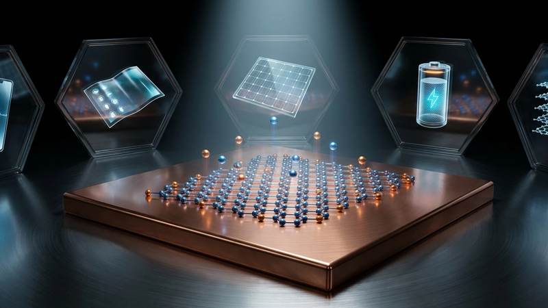
Section 6: Future Horizons & High-Value B2B Applications
The trajectory of graphene synthesis via chemical vapor deposition on copper substrates points towards increasingly refined control over material properties and the integration of advanced functionalities, paving the way for unprecedented B2B applications. Future horizons in CVD research are centered on atomic-scale defect engineering, precise layer count control across wafer-scale areas, and the development of in-situ monitoring techniques to optimize growth kinetics. This includes exploring novel catalyst alloys beyond pure copper, such as Cu-Ni or Cu-Pt, which offer tailored carbon solubility and nucleation densities, enabling the growth of specific graphene polytypes or turbostratic stacking. Furthermore, the integration of rapid thermal processing, employing localized thermal pulses exceeding 3000K for milliseconds, is being investigated to enhance crystallinity and reduce grain boundary density post-growth, directly translating to improved electrical and mechanical performance for subsequent device fabrication. The advent of roll-to-roll CVD systems, already demonstrating capabilities for continuous graphene production on meter-long copper foils, signifies a critical step towards industrial scalability, driving down manufacturing costs and expanding access to high-quality graphene for diverse sectors.
In advanced electronics, the high-value applications of CVD graphene are poised to revolutionize several domains. Its exceptional carrier mobility, often exceeding 5,000 cm^2/Vs even on amorphous substrates, positions it as a critical enabler for terahertz frequency electronics, with prototype graphene field-effect transistors demonstrating cut-off frequencies approaching 400 GHz, far surpassing conventional silicon limits in certain high-frequency applications. For transparent conductive films, CVD graphene offers a compelling alternative to indium tin oxide (ITO), exhibiting sheet resistances below 100 Ohm/sq at 90% optical transmittance, with superior flexibility and mechanical robustness essential for foldable displays, wearable electronics, and smart windows. The low electrical resistivity, measured in the range of 10^-6 Ohm·cm for high-quality single-layer material, coupled with its atomic thickness, facilitates the development of ultrathin, lightweight interconnects and electrodes for next-generation integrated circuits and photovoltaic devices, where efficient charge transport and minimal material consumption are paramount.
Beyond electronics, the unique properties of CVD graphene on copper underpin its immense potential in energy storage, environmental remediation, and advanced materials. In energy, graphene-based supercapacitors are demonstrating specific capacitance values exceeding 200 F/g, offering high power density, rapid charge/discharge rates, and extended cycle life (over 100,000 cycles with minimal degradation) for electric vehicles and grid-scale energy storage. For environmental applications, functionalized CVD graphene membranes exhibit exceptional selectivity for ion sieving and gas separation, with empirical data showing heavy metal adsorption efficiencies reaching 79% for lead and cadmium ions in aqueous solutions, leveraging its high surface area and tunable surface chemistry for water purification. Furthermore, its impermeability to even the smallest gas molecules and remarkable mechanical strength make it an ideal candidate for protective coatings against corrosion and wear in harsh industrial environments, extending the lifespan of critical infrastructure components and reducing maintenance costs in industries ranging from aerospace to marine.
Evaluate Our Quality
Serious about B2B integration? Test our premium Pulsed Electrical Resistive Carbon Heating turbostratic graphene in your lab. 100g sample packs available now.