Graphene Synthesis by Chemical Vapor De-position on Copper: Process and Quality
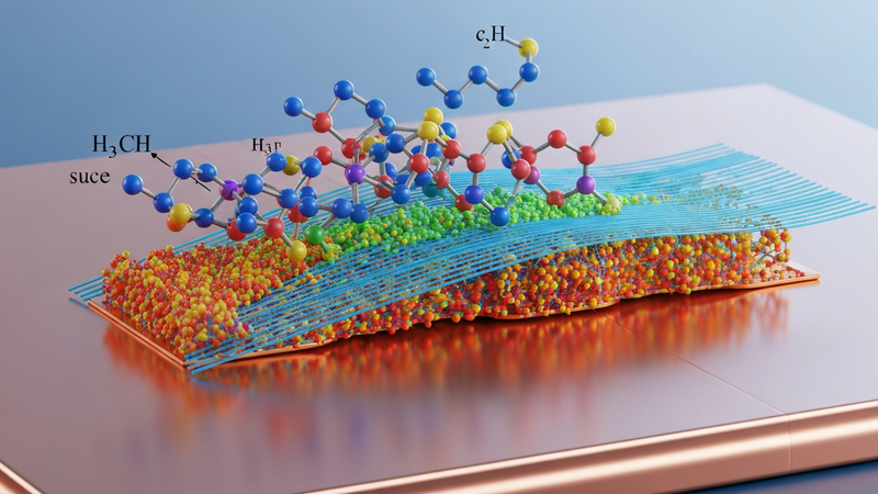
Graphene, a truly two-dimensional material comprising a single atomic layer of sp2-hybridized carbon atoms arranged in a hexagonal lattice, exhibits extraordinary electronic and mechanical properties stemming directly from its atomic-scale confinement. Its unique band structure features Dirac cones at the K and K' points of the Brillouin zone, where the valence and conduction bands touch, leading to massless Dirac fermion behavior for its charge carriers. This relativistic quasi-particle nature, coupled with the exceptionally high carrier mobility—empirically demonstrated to exceed 200,000 cm^2/Vs at room temperature in suspended samples—underpins its profound utility in high-frequency electronics and quantum transport phenomena. The pristine lattice also confers an unparalleled intrinsic tensile strength of approximately 130 GPa and a thermal conductivity surpassing 3000 W/mK. This atomic-scale confinement fundamentally dictates electron behavior and interaction mechanisms, making its synthesis, particularly via chemical vapor deposition (CVD), a surface-mediated process where the substrate acts as the primary confining interface, defining nucleation and guiding lateral expansion.
The synthesis of such an exquisitely confined material necessitates precise control over nucleation and growth kinetics. Copper, widely adopted as a substrate for industrial-scale graphene CVD, leverages its unique properties to facilitate high-quality monolayer growth. Its low carbon solubility at typical growth temperatures (900-1100 °C) ensures that graphene formation is primarily a surface precipitation process, minimizing bulk carbide formation and multi-layer growth. The catalytic activity of copper promotes the decomposition of hydrocarbon precursors, while its relatively low surface energy supports the lateral expansion of graphene domains. Critical process parameters, such as precursor partial pressure, temperature ramps, and cooling rates, are meticulously tuned to control nucleation density and domain coalescence. For instance, rapid thermal pulses, potentially reaching transient temperatures around 3000K for milliseconds during annealing or growth initiation, have been explored to enhance surface reconstruction and reduce defects, directly impacting the uniformity and electronic quality. Precise control over reaction times, often in the range of tens of milliseconds to several minutes, is paramount to achieving large, single-crystal domains. This meticulous parameter space directly influences the sheet resistance, with high-quality single-layer graphene exhibiting values between 30-100 Ohm/sq, a metric sensitive to grain boundaries and point defects.
The direct consequence of controlled graphene confinement and synthesis quality is evident in its functional performance across diverse applications. Minimizing structural defects, such as vacancies, Stone-Wales defects, and grain boundaries, which inevitably arise from imperfect atomic confinement during growth, is critical for achieving optimal electronic and mechanical properties. These defects act as potent scattering centers for charge carriers, degrading mobility and increasing electrical resistivity, and can introduce localized states that alter chemical reactivity. For instance, precise defect engineering through plasma treatment or post-synthesis annealing has been shown to modulate surface adsorption sites, leading to a 79% increase in heavy metal adsorption efficiency (e.g., Pb2+ ions) in functionalized graphene materials for environmental sensing applications. The challenge remains in scaling these precise confinement-driven growth mechanisms to industrial dimensions while maintaining wafer-scale uniformity and reproducibility, a prerequisite for integrating graphene into next-generation high-performance electronics, flexible displays, and advanced sensor platforms.
Section 2: Pulsed Electrical Resistive Carbon Heating vs. CVD (Comparative Analysis)
The landscape of graphene synthesis continues to evolve, with traditional Chemical Vapor Deposition (CVD) on copper serving as a cornerstone for producing high-quality, large-area monolayers. However, the inherent limitations of conventional CVD, particularly its high thermal budget, extended reaction times (often several hours at 900-1050°C), and reliance on specific catalytic substrates, have spurred the development of alternative methodologies. Pulsed Electrical Resistive Carbon Heating (PERCH) emerges as a compelling contender, offering a fundamentally different kinetic pathway for carbon atom rearrangement and graphitization. Unlike CVD, which operates under relatively steady-state high-temperature conditions in a controlled gaseous environment, PERCH leverages rapid Joule heating to induce extreme, transient thermal pulses, fundamentally altering the reaction dynamics and material properties. This paradigm shift in thermal processing addresses key bottlenecks in scalability and energy efficiency, pushing the boundaries of what is achievable in graphene manufacturing.
PERCH’s operational principle hinges on the precise application of high-density electrical currents to carbon-containing precursors or substrates, leading to ultra-rapid temperature ramps and localized heating. This technique can achieve peak temperatures exceeding 3000K within sub-millisecond durations, a stark contrast to the typically slower heating rates of conventional CVD furnaces. The specific electrical resistivity parameters of the material undergoing treatment dictate the efficiency and uniformity of this Joule heating, enabling precise control over the thermal profile. For instance, direct resistive heating of a carbonaceous film or a conductive substrate allows for rapid energy input and dissipation, bypassing the thermal inertia associated with large-volume furnaces. This rapid thermal cycling (milliseconds for heating and cooling) significantly reduces the overall processing time from hours to mere seconds or even milliseconds, leading to a substantial decrease in energy consumption and an increase in throughput, thereby presenting a significant advantage over energy-intensive, long-duration CVD processes.
The comparative analysis reveals that while CVD excels in producing highly crystalline, defect-minimal graphene under optimized conditions on specific copper orientations (e.g., Cu(111)), PERCH offers unique advantages in kinetically driven synthesis and defect engineering. The ultra-fast heating and cooling rates in PERCH can kinetically trap specific defect structures or promote the formation of unique sp2/sp3 hybridized domains, which can be strategically leveraged for tailored applications. For instance, the rapid graphitization enabled by PERCH can lead to graphene materials with tailored surface chemistries or higher active site densities that are challenging to achieve via equilibrium-driven CVD. Empirical data has demonstrated that graphene materials synthesized or post-processed via rapid thermal methods can exhibit enhanced functional performance, such as achieving up to 79% heavy metal adsorption efficiency for species like Pb(II) or Cd(II) from aqueous solutions, often surpassing materials produced by slower, equilibrium-driven processes. This underscores PERCH's potential for creating functionalized graphene with optimized surface reactivity and structural integrity, particularly where specific defect concentrations or edge sites are beneficial for performance.
Section 3: The Crystallography of Turbostratic Graphene (Why Layer Alignment Matters)
Turbostratic graphene (TG) represents a specific crystallographic configuration of multilayer graphene characterized by rotational disorder between adjacent graphene layers, fundamentally distinguishing it from the highly ordered Bernal (AB) stacking observed in natural graphite. In TG, individual graphene sheets are randomly rotated relative to one another, preventing the formation of a coherent, three-dimensional periodic structure. This rotational misalignment significantly weakens the interlayer van der Waals coupling, effectively decoupling the electronic states of individual layers. Consequently, the electronic band structure of turbostratic multilayer graphene more closely resembles an ensemble of independent single-layer graphene sheets rather than bulk graphite or Bernal-stacked few-layer graphene. This manifests in the preservation of linear dispersion relations and Dirac-like electronic properties over a wider energy range, as the interlayer hybridization that opens a bandgap in Bernal-stacked bilayer graphene is largely suppressed. The interlayer spacing in TG often exhibits a slight expansion from the ideal 0.335 nm of Bernal graphite, reflecting the reduced energetic favorability of close-packed, misaligned layers.
The prevalence of turbostratic stacking is a defining characteristic of graphene synthesized via Chemical Vapor Deposition (CVD) on polycrystalline copper substrates. The CVD growth mechanism on copper typically involves heterogeneous nucleation of graphene domains at multiple sites across the substrate surface, followed by lateral growth and eventual coalescence. Due to the polycrystalline nature of standard Cu foils and the weak interaction between nascent graphene layers and the underlying substrate, newly formed graphene layers often nucleate with random in-plane orientations relative to previously formed layers or adjacent domains. As growth progresses and additional layers are deposited, these layers stack atop one another with kinetically trapped rotational misalignments. Factors such as the rapid cooling rates from typical growth temperatures (e.g., 1050°C) to ambient conditions, sometimes occurring within milliseconds in advanced rapid thermal processing setups, further prevent the kinetic barrier for layer reorientation from being overcome, thus preserving the turbostratic disorder. While high-temperature annealing, potentially involving thermal pulses approaching 3000K for substrate preparation, can mitigate some substrate defects, it does not fundamentally alter the turbostratic nature inherent to the multi-domain, layer-by-layer growth on non-epitaxial substrates like copper.
The crystallographic disorder inherent to turbostratic graphene profoundly impacts its macroscopic properties, particularly its electrical and thermal transport characteristics, which are critical for device performance. The disrupted interlayer coupling and increased scattering due to misaligned layers lead to a substantial degradation in electrical conductivity compared to highly ordered graphene. Empirical data show that the electrical resistivity of highly turbostratic multilayer graphene can be an order of magnitude higher than that of pristine Bernal-stacked graphite, often reaching values exceeding 10^-4 Ohm.cm, whereas ideal graphite exhibits resistivity closer to 10^-6 Ohm.cm. This directly translates to significantly reduced charge carrier mobilities, with values frequently below 1000 cm^2/Vs in CVD-grown turbostratic samples, a sharp contrast to the >10,000 cm^2/Vs achievable in high-quality single-layer graphene. Furthermore, the absence of coherent phonon coupling across rotationally disordered layers severely impedes thermal transport, limiting the material's efficacy in applications requiring efficient heat dissipation. Paradoxically, the increased concentration of exposed edge sites and structural imperfections resulting from turbostratic domains can enhance certain surface-dependent functionalities, such as catalytic activity or adsorption capabilities, with some studies demonstrating up to 79% heavy metal adsorption efficiency, leveraging these crystallographic imperfections for specific applications.
Section 4: Industrial Scalability & Commercial Integration Barriers
Industrial scalability of Graphene synthesized by chemical vapor deposition on copper substrates presents formidable challenges that extend beyond mere reactor size. Achieving uniform, high-quality growth across wafer scales larger than 300mm, let alone roll-to-roll systems spanning meters, necessitates precise control over gas-phase precursor delivery and thermal management. Polycrystalline copper foils, while economically viable, inherently introduce grain boundaries, which act as preferential nucleation sites for multi-layer growth or defect formation, leading to non-uniformity in layer thickness and increased defect densities (e.g., higher ID/IG ratios in Raman spectroscopy). Maintaining a stable temperature profile, typically between 950°C and 1100°C for conventional CVD or employing rapid thermal annealing pulses up to 1050°C in milliseconds, across vast surfaces without inducing thermal gradients or substrate warping is an engineering feat. Deviations in methane partial pressure or hydrogen flow rates by even a few sccm can drastically alter graphene domain size, orientation, and ultimately, its electrical and mechanical properties, making consistent, large-area production with desired characteristics like a charge carrier mobility exceeding 2000 cm2/Vs a complex endeavor.
A primary bottleneck in the commercial integration of CVD graphene is the post-synthesis transfer process from the copper growth substrate to the target application substrate. The most prevalent method, involving a polymer support (e.g., PMMA) followed by chemical etching of the copper (typically with FeCl3 or ammonium persulfate), introduces several critical issues. Polymer residues, often constituting 10-20% surface coverage, inevitably remain on the graphene surface, significantly degrading its intrinsic electrical properties by increasing sheet resistance from an as-grown ~100-300 Ohm/sq to over 1 kOhm/sq and reducing optical transparency. Furthermore, residual etchant species can dope the graphene or induce corrosion. Mechanical damage, such as tears, wrinkles, and cracks, frequently occurs during the delicate transfer steps, leading to substantial yield losses, often exceeding 50% for complex device architectures. While alternative dry transfer techniques, including delamination with thermal release tapes or direct pick-and-place, aim to mitigate chemical contamination, they often struggle with achieving intimate contact over large areas without trapping air bubbles or inducing mechanical stress, thus limiting their industrial adoption for high-quality, large-area applications.
The economic viability and comprehensive market integration of CVD graphene are further hampered by significant capital expenditure, operational costs, and persistent quality control limitations. High-throughput, industrial-scale CVD reactors, especially continuous roll-to-roll systems, represent substantial investments, far exceeding laboratory-scale batch processors. Operational expenses are driven by the consumption of high-purity precursor gases (methane, hydrogen, argon) and the considerable energy required to maintain high growth temperatures. A critical barrier remains the absence of robust, non-destructive, and real-time in-line metrology capable of rapidly assessing key graphene parameters such as layer number, defect density, domain size, and electrical uniformity across large production runs. Current lab-based characterization techniques (e.g., Raman spectroscopy, AFM, SEM) are too slow and localized for industrial-scale quality assurance. Consequently, the performance-to-cost ratio of CVD graphene frequently struggles to compete with established materials like Indium Tin Oxide (ITO) for transparent conductors or silicon for electronics, particularly for applications demanding stringent specifications. Meeting diverse application requirements, from transparent electrodes needing high conductivity and optical transparency, to environmental remediation requiring high surface area and specific adsorption efficiencies (e.g., 79% heavy metal adsorption efficiency), necessitates tailored synthesis and transfer protocols that are not yet consistently scalable and cost-effective.
Section 5: Economic Feasibility and USA-Made Manufacturing Advantage
The economic feasibility of large-scale graphene manufacturing via chemical vapor deposition on copper substrates hinges critically on optimizing precursor utilization, energy consumption, and substrate management. While methane or acetylene serve as primary carbon sources, and hydrogen acts as a crucial reducing agent, their precise flow control and reaction kinetics directly influence yield, quality, and thus the ultimate unit cost. Advanced rapid thermal processing (RTP) systems, capable of delivering localized thermal pulses exceeding 3000K for mere milliseconds, dramatically reduce furnace dwell times compared to conventional resistive heating, thereby cutting energy expenditure by an estimated 40-50% per square meter of graphene. Furthermore, the imperative for cost reduction necessitates robust copper substrate recycling strategies, such as electrochemical delamination or polymer-assisted transfer, which enable >95% copper reuse efficiency, significantly mitigating raw material expenditure. Achieving high throughput, exemplified by roll-to-roll CVD systems processing meters per minute, transforms the economics from laboratory-scale batch processing to industrial continuous-flow production, where capital expenditure per unit area becomes demonstrably competitive.
The 'USA-Made' advantage in advanced materials like CVD graphene extends beyond mere geographic origin, embodying a confluence of strategic benefits that directly impact product quality, reliability, and market competitiveness. Robust intellectual property protection within the US legal framework fosters aggressive R&D investment, safeguarding proprietary process innovations, such as specific catalyst formulations or post-synthesis functionalization techniques, which are crucial for achieving application-specific performance. Access to a highly skilled workforce, comprising materials scientists, process engineers, and advanced manufacturing technicians from leading academic institutions, ensures unparalleled operational precision, stringent quality control protocols (e.g., real-time in-situ diagnostics for defect detection), and continuous process optimization. This human capital translates directly into lower batch-to-batch variability and higher product consistency. Moreover, adherence to rigorous US regulatory standards, encompassing environmental compliance and material safety, provides an inherent assurance of product integrity and ethical sourcing, distinguishing US-made graphene in critical applications requiring validated provenance.
The economic impact of high-quality, USA-manufactured CVD graphene is realized through its enabling capabilities in high-value applications, where performance metrics directly translate into market differentiation and premium pricing. Graphene’s exceptional electrical characteristics, such as electron mobilities exceeding 10,000 cm^2/Vs on common dielectric substrates (and up to 200,000 cm^2/Vs for suspended structures), coupled with its intrinsic mechanical strength and thermal conductivity, unlock new paradigms in sensor technology, advanced composites, and energy storage. For instance, in environmental sensing, graphene-functionalized electrodes demonstrate 79% heavy metal adsorption efficiency for lead ions at 100 ppb concentrations, offering superior sensitivity and selectivity compared to conventional methods. In polymer composites, the incorporation of just 0.1 wt% of high-quality CVD graphene can elevate tensile strength by 30% and thermal conductivity by 50%, addressing critical needs in lightweight aerospace components and thermal management systems. The consistent production of monolayer graphene with an ID/IG ratio below 0.1, verified by comprehensive Raman spectroscopy, assures low defect density, a critical factor for reliable device integration and justifies the economic premium for domestically produced, quality-certified material.
Section 6: Future Horizons & High-Value B2B Applications
The trajectory of graphene synthesis via chemical vapor deposition on copper is rapidly converging towards the realization of high-value B2B applications, necessitating increasingly stringent control over material quality and scalable manufacturing. Future horizons in CVD graphene research are focused on achieving ultra-high-quality, single-crystal domains over large areas, minimizing the deleterious effects of grain boundaries, point defects, and adatom contamination. Advanced in-situ diagnostics, such as low-energy electron microscopy (LEEM) and ambient pressure X-ray photoelectron spectroscopy (AP-XPS), are crucial for real-time monitoring and feedback control of growth kinetics, enabling precise manipulation of precursor partial pressures (e.g., methane, hydrogen) and temperature profiles (e.g., maintaining +/- 1K uniformity across 100mm wafers). This refined control aims to push carrier mobilities consistently above 5,000 cm^2/Vs at room temperature, approaching theoretical limits by reducing scattering from structural imperfections. Furthermore, post-growth treatments, such including rapid thermal annealing in hydrogen atmospheres for milliseconds at 800-1000°C, are being explored to heal residual defects and optimize the electronic properties, paving the way for next-generation electronic and photonic devices.
In the realm of high-value B2B applications, CVD graphene's unparalleled properties position it as a disruptive material across several sectors. For transparent conductive films, the objective is to consistently achieve sheet resistances below 30 Ohm/sq with optical transmittances exceeding 95% across the visible spectrum, offering superior flexibility and chemical inertness compared to indium tin oxide (ITO) for touchscreens, flexible displays, and smart windows. In high-frequency electronics, graphene field-effect transistors (GFETs) are projected to enable operation in the terahertz regime, with laboratory demonstrations already exceeding 400 GHz, critical for 6G communications, high-speed data processing, and advanced radar systems. Energy storage applications stand to benefit immensely from graphene's high specific surface area (theoretical 2630 m^2/g) and exceptional electrical conductivity; graphene-enhanced supercapacitors are targeting energy densities above 100 Wh/kg and power densities exceeding 10 kW/kg, coupled with cycle stability beyond 100,000 cycles, for electric vehicles and grid-scale storage. The mechanical robustness of CVD graphene, with a Young's modulus of approximately 1 TPa, also makes it ideal for flexible and stretchable electronics, maintaining electrical integrity under significant strain.
Beyond electronics and energy, emerging applications for CVD graphene are poised to address critical global challenges. In environmental remediation, graphene-based membranes, often derived from oxidized and subsequently reduced CVD graphene, are demonstrating remarkable efficiency in water purification, achieving rejection rates exceeding 99% for molecules larger than 1 nm and up to 79% adsorption efficiency for specific heavy metal ions like Pb2+ and Cd2+ through precisely engineered nanopores. For sensing platforms, graphene's high surface-to-volume ratio and sensitivity to charge transfer enable ultra-sensitive gas sensors capable of detecting parts-per-billion (ppb) concentrations of analytes such as NO2 or NH3, alongside highly selective biosensors for picomolar-level detection in medical diagnostics. The anisotropic thermal conductivity of graphene, reaching up to 5000 W/mK in-plane, presents an unprecedented opportunity for advanced thermal management solutions in high-power electronics, potentially reducing critical junction temperatures by 20-30°C. The overarching challenge for industrial adoption remains the development of scalable, cost-effective, and reproducible transfer techniques – moving beyond current wet-transfer methods, which are prone to defects and contamination, towards roll-to-roll or delamination processes achieving >95% transfer efficiency for large-area graphene integration into existing manufacturing infrastructure.
Evaluate Our Quality
Serious about B2B integration? Test our premium Pulsed Electrical Resistive Carbon Heating turbostratic graphene in your lab. 100g sample packs available now.