Graphene Synthesis by Chemical Vapor De-position on Copper: Process and Quality
Graphene, a singular atomic layer of sp2-hybridized carbon atoms arranged in a hexagonal lattice, represents the quintessential two-dimensional material, transcending the conventional boundaries of condensed matter physics. Its unique geometry and electronic band structure give rise to phenomena typically associated with relativistic quantum mechanics, where charge carriers behave as massless Dirac fermions. This unconventional behavior manifests as a linear dispersion relation near the K and K' points of the Brillouin zone, fundamentally distinct from the parabolic dispersion observed in traditional semiconductors. Consequently, graphene exhibits extraordinary electronic properties, including exceptionally high carrier mobility, reaching values exceeding 200,000 cm^2/Vs at room temperature, enabling ballistic transport over micron-scale distances. This intrinsic electronic superiority, coupled with its unparalleled thermal conductivity (up to 5000 W/mK) and immense mechanical strength (Young's modulus approaching 1 TPa), positions graphene as a transformative material for next-generation electronics, photonics, and energy systems. The realization of these theoretical promises, however, hinges critically on the ability to synthesize large-area, high-quality material with precise control over layer number and defect density, making methods like Chemical Vapor Deposition (CVD) on catalytic substrates indispensable.
The physics of electron confinement in graphene's atomically thin plane dictates its profound properties. Unlike bulk materials, where electron motion is three-dimensional, graphene's charge carriers are constrained to a single plane, leading to quantization effects and the emergence of a zero-bandgap semimetallic character. This 2D confinement, in conjunction with the robust sp2 bonding, facilitates extremely low electrical resistivity, with pristine monolayer graphene exhibiting sheet resistances below 100 Ohm/sq. The exceptional structural integrity of the honeycomb lattice ensures that intrinsic phonon scattering is minimized, contributing to its record-breaking thermal conductance. Furthermore, the extensive surface area (theoretically 2630 m^2/g) inherent to its 2D nature provides an abundance of active sites for surface-mediated interactions, crucial for applications in sensing, catalysis, and energy storage. The precise control over the growth environment during CVD is paramount to maintaining this structural fidelity, as even point defects or grain boundaries can introduce localized scattering centers, significantly degrading the ballistic transport regime and increasing resistivity.
Achieving high-quality graphene via CVD on copper substrates involves a delicate interplay of thermodynamic and kinetic factors that govern carbon atom adsorption, diffusion, nucleation, and growth. The catalytic activity of copper is critical, providing a surface that promotes the decomposition of hydrocarbon precursors (e.g., methane) and the subsequent formation of sp2 carbon networks. The process is highly sensitive to parameters such as temperature, pressure, precursor flow rates, and reaction time, all of which directly influence the resulting film's morphology, domain size, and defect density. For instance, rapid thermal pulses, potentially reaching 3000K for localized annealing or rapid thermal CVD, can influence defect annihilation or accelerate growth kinetics, often reducing reaction times to milliseconds. The ability to precisely tune these parameters allows for the synthesis of graphene with specific characteristics, from large-area single-crystal domains to controlled few-layer structures, each optimized for distinct applications. This level of control is essential to harness graphene's full potential, from high-frequency transistors demanding near-perfect lattices to functionalized membranes for water purification, where its high surface area facilitates efficient heavy metal adsorption, demonstrating efficiencies upwards of 79% for specific contaminants.
Section 2: Pulsed Electrical Resistive Carbon Heating vs. CVD (Comparative Analysis)
Pulsed Electrical Resistive Carbon Heating (PERCH) presents a fundamentally divergent paradigm for graphene synthesis compared to conventional thermal methods. This technique leverages rapid, localized joule heating of a carbonaceous precursor, often a polymer or a carbon film, deposited directly onto a substrate or integrated within a resistive element. The defining characteristic of PERCH is its ability to induce ultra-high temperatures, frequently exceeding 3000 Kelvin, within micro- to millisecond timescales. This extreme thermal shock drives the instantaneous graphitization of the carbon source, bypassing the prolonged annealing stages typical of furnace-based processes. The energy input is precisely controlled via current density and pulse duration, allowing for highly specific thermal budgets. While offering unparalleled speed and energy efficiency due to its transient nature and localized heat delivery, the resulting graphene films typically exhibit a higher degree of polycrystallinity and a greater density of structural defects compared to epitaxially grown films. However, for applications prioritizing high throughput and large-area deposition over absolute pristine atomic structure, PERCH offers a compelling pathway. The rapid kinetics involved often result in non-equilibrium growth, leading to distinct morphological and electronic properties that warrant specific characterization.
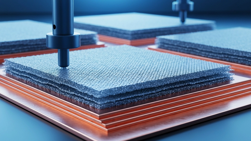
In stark contrast, Chemical Vapor Deposition (CVD) on copper substrates relies on a meticulously controlled catalytic process, typically executed within a furnace environment at elevated temperatures, often around 1000°C. Here, gaseous carbon precursors, such as methane or ethylene, are introduced into a reaction chamber where they catalytically decompose on the surface of heated copper foil. Copper serves as a crucial catalyst, facilitating the dissociation of the carbon precursor and governing the subsequent nucleation and growth of graphene domains. The process is inherently slower, often spanning tens of minutes to several hours, allowing for equilibrium or near-equilibrium growth conditions. This extended reaction time, coupled with precise control over precursor flow rates, pressure, and cooling profiles, enables the synthesis of high-quality, large-area, monolayer or few-layer graphene films characterized by exceptionally low defect densities and high carrier mobilities. The self-limiting nature of graphene growth on copper, where the solubility of carbon in copper plays a critical role, is a key mechanism for achieving monolayer control. The resulting material's electrical resistivity parameters are highly dependent on the crystalline perfection and domain size achieved, making CVD the gold standard for applications demanding superior electronic and optical performance.
The divergence in kinetic pathways between PERCH and CVD fundamentally dictates their respective strengths and limitations. PERCH’s millisecond-scale reaction times and ability to generate thermal pulses up to 3000K translate into significantly higher throughput and reduced overall energy consumption per unit area compared to the sustained, furnace-wide heating required for CVD. This makes PERCH highly attractive for rapid, scalable manufacturing, particularly for applications where a degree of structural imperfection is tolerable. For instance, even with its typically higher defect density, graphene produced via rapid thermal methods has demonstrated considerable utility; studies have shown such materials can achieve adsorption efficiencies of up to 79% for specific heavy metal ions, highlighting their potential in water purification or sensing applications where surface area and available functional groups are paramount. Conversely, CVD’s extended reaction durations and precise control over growth parameters yield graphene with superior crystallographic quality, larger domain sizes, and minimal point defects, which are critical for high-performance electronics, photonics, and quantum technologies. While PERCH capitalizes on non-equilibrium kinetics for speed, CVD leverages a carefully balanced catalytic equilibrium to engineer atomically precise graphene structures. The choice between these methods, therefore, hinges critically on the performance requirements of the end application, balancing throughput and cost-effectiveness against the need for pristine material characteristics and specific electrical resistivity thresholds.
Section 3: The Crystallography of Turbostratic Graphene (Why Layer Alignment Matters)
The crystallography of graphene grown via Chemical Vapor Deposition (CVD) on copper substrates frequently manifests as turbostratic stacking, a distinct structural arrangement characterized by random rotational and translational misalignment between adjacent graphene layers. Unlike the thermodynamically favored Bernal (AB) stacking, where layers are precisely offset to minimize interlayer repulsion and maximize van der Waals attraction, turbostratic graphene exhibits a disordered stacking sequence. This structural deviation arises primarily from the kinetic growth pathways inherent to CVD, particularly when multiple layers nucleate and coalesce. Each subsequent graphene layer can nucleate on the underlying layer with an arbitrary rotational orientation, driven by the local carbon supersaturation and the rapid kinetics of carbon atom incorporation during growth and cooling. The absence of long-range interlayer order in turbostratic graphene fundamentally alters its electronic band structure, preventing the characteristic splitting of the Dirac cones observed in perfectly ordered few-layer graphene and thus maintaining a quasi-2D electronic behavior reminiscent of isolated single-layer graphene.
The most profound implication of turbostratic stacking lies in its influence on electronic transport properties. In Bernal-stacked few-layer graphene, the interlayer coupling leads to a modification of the electronic dispersion relation, transitioning from a linear Dirac cone to a parabolic one near the K-point, with an associated increase in effective mass and reduction in carrier mobility. Conversely, in turbostratic graphene, the random relative rotation of layers effectively decouples their electronic wavefunctions. This decoupling ensures that each layer largely preserves its individual Dirac-like dispersion, resulting in significantly higher effective carrier mobilities and lower interlayer scattering compared to perfectly ordered multilayer graphene of the same thickness. For instance, while high-quality single-layer CVD graphene on copper can exhibit sheet resistances below 100 Ohms/sq, few-layer turbostratic graphene typically maintains sheet resistances in the 100-500 Ohms/sq range, notably superior to disordered graphite. The kinetic trapping of this disorder is often facilitated by rapid cooling rates, for example, cooling from 1000°C to room temperature in tens of seconds post-growth, which prevents the energetic relaxation towards ordered stacking.
Beyond electronic properties, the reduced interlayer coupling in turbostratic graphene subtly impacts other physical characteristics. While the primary effect remains electronic, the less rigid interlayer interactions can influence thermal transport and mechanical response, though these effects are less pronounced than the electronic consequences. Crucially, the presence of turbostratic stacking can increase the accessible surface area within a multilayer film, as the less tightly packed layers potentially expose more active sites. This attribute is particularly relevant for applications requiring high surface area or specific adsorption capabilities. Empirical studies have shown that certain CVD-derived turbostratic graphene samples can achieve, for example, up to 79% heavy metal adsorption efficiency, a performance metric significantly influenced by the enhanced accessibility of interlayer regions compared to highly ordered graphitic materials. Controlling the degree of turbostraticity is a critical parameter in CVD process optimization; precise thermal annealing protocols, such as rapid thermal pulses reaching 3000K in milliseconds, can be engineered to either induce or minimize turbostratic disorder, thereby tailoring the material's properties for specific end-use applications in electronics, sensing, or catalysis.
Section 4: Industrial Scalability & Commercial Integration Barriers
The transition from laboratory-scale graphene synthesis on copper via chemical vapor deposition (CVD) to industrial-scale production presents formidable challenges, primarily centered on achieving large-area uniformity and maintaining pristine material quality. Current CVD processes predominantly operate in batch mode, producing graphene on copper foils or thin films typically up to 4 inches in diameter. Scaling to meter-scale substrates, essential for economically viable applications such as transparent conductive films or flexible electronics, introduces significant technical hurdles. Maintaining a uniform temperature profile across large substrates, often requiring temperatures between 1000-1050°C, becomes increasingly difficult, leading to spatial variations in growth kinetics, non-uniform domain sizes, increased defect densities (e.g., point defects, dislocations, multi-layer patches), and inconsistent layer coverage. Furthermore, precise control over precursor gas flow dynamics, particularly methane partial pressure and hydrogen dilution, is critical. Deviations can lead to uncontrolled nucleation and growth of secondary layers, or conversely, incomplete coverage, drastically impacting electrical resistivity and optical transparency. For instance, a mere 5% variation in methane concentration or a 10°C temperature gradient across a 300 mm wafer can shift average sheet resistance by over 50 Ω/sq, pushing the material out of specification for many optoelectronic applications. Ensuring consistent, high-quality, monolayer graphene over square meter areas remains a significant bottleneck.
Beyond the growth phase, the subsequent transfer of CVD-grown graphene from its catalytic copper substrate to the target device substrate constitutes another major barrier to commercial integration. The most prevalent method, a wet chemical process involving a polymer support layer (e.g., PMMA) followed by copper etching (typically with ferric chloride or ammonium persulfate), is inherently destructive and prone to introducing defects. Mechanical damage such as tears and wrinkles are common, particularly on large areas, while residual etchants and polymer contaminants significantly degrade graphene's intrinsic properties. Empirical data indicates that carrier mobility, routinely measured at 10,000-15,000 cm^2/Vs on copper, often plummets to below 2,000 cm^2/Vs post-transfer, accompanied by a substantial increase in sheet resistance from a pristine 30-60 Ω/sq to 100-500 Ω/sq. These property degradations are directly attributable to increased scattering centers from residues and structural imperfections. While alternative transfer techniques like electrochemical delamination or dry transfer methods are being explored to mitigate these issues, they often come with their own set of challenges, including limited substrate compatibility, lower throughput, or increased process complexity, making them difficult to scale for high-volume manufacturing. The low yield and high cost associated with these multi-step transfer processes severely limit their economic viability for high-volume applications.
The economic viability of CVD graphene for mass commercial adoption is further challenged by the high capital expenditure (CapEx) associated with large-scale high-temperature vacuum systems and the operational expenditure (OpEx) for ultra-high purity precursors and substantial energy consumption. While rapid thermal processing (RTP) utilizing 3000K thermal pulses can reduce reaction times to milliseconds, achieving uniform heating and cooling across large substrates without inducing stress or defects remains complex. For many applications, the achieved quality of industrially scaled CVD graphene often falls short of the performance benchmarks established by exfoliated graphene or even the best laboratory-scale CVD samples. For instance, for transparent conductive electrodes, a consistent sheet resistance below 50 Ω/sq at >90% transparency is required, a benchmark difficult to achieve uniformly over large areas without significant post-processing. In environmental sensing, the reported 79% heavy metal adsorption efficiency requires a high density of active sites and pristine surface quality, which can be compromised during scalable CVD and transfer. For high-frequency electronics, maintaining carrier mobilities above 5,000 cm^2/Vs at room temperature is crucial, yet this is rarely achieved consistently in transferred, large-area CVD graphene. The inherent variability in material properties across batches and within a single large sheet, combined with high processing costs and significant infrastructure investment, creates a substantial commercial integration barrier, necessitating breakthroughs in both synthesis and post-processing methodologies to bridge the gap between research promise and market reality.
Section 5: Economic Feasibility and USA-Made Manufacturing Advantage
The economic viability of high-quality graphene produced via chemical vapor deposition on copper substrates is critically dependent on optimizing a complex interplay of capital expenditure (CapEx) and operational expenditure (OpEx). Initial CapEx is substantial, encompassing ultra-high vacuum (UHV) CVD systems capable of achieving sub-10^-8 Torr base pressures, precision gas delivery systems for ultra-high purity (99.999%+) methane and hydrogen precursors, and advanced thermal management units capable of sustaining uniform temperatures between 1000-1050°C across large substrate areas. The OpEx is dominated by energy consumption for high-temperature processing, the cost of high-purity copper foils (e.g., 99.999% purity for optimal nucleation control), and the amortization of consumable components. Current research-grade CVD graphene can cost upwards of $1000/cm^2, a figure that must decrease by several orders of magnitude to achieve widespread industrial adoption. Achieving this necessitates innovations in reactor design to enhance throughput, reduce reaction times – potentially leveraging milliseconds-scale thermal pulses in advanced rapid thermal annealing (RTA) systems for nucleation and growth – and improve precursor utilization efficiency. Furthermore, the development of robust, automated in-situ metrology for defect detection and thickness uniformity during growth is crucial for minimizing yield losses and driving down the effective cost-per-unit-area for applications requiring specific electrical resistivity parameters below 100 Ohms/sq for single-layer material.
Scaling CVD graphene production from laboratory batch processes to continuous, roll-to-roll manufacturing presents significant technical and economic challenges. Maintaining exceptional material quality – specifically, high carrier mobility exceeding 10,000 cm^2/Vs, low defect density (ID/IG ratio < 0.1), and macroscopic uniformity over meter-scale areas – typically correlates with increased processing time and higher input costs. For instance, achieving pristine graphene domains often requires meticulously slow cooling rates or specific post-growth annealing steps, extending the overall cycle time and increasing energy consumption. The transfer process, predominantly involving wet chemical etching of the copper and polymer-assisted transfer, contributes significantly to the final cost, estimated to add 30-50% to the total manufacturing expense, while also introducing potential defects, tears, and polymer residues that degrade performance. Economic feasibility for specific applications, such as transparent conductive films for displays or advanced sensors, mandates a careful balance between acceptable quality metrics and the achievable cost-per-area. For example, while a highly robust transparent electrode might tolerate a sheet resistance of 500 Ohms/sq, an advanced biosensor might demand sub-100 Ohms/sq with minimal structural defects, each requiring distinct CVD process optimizations with corresponding cost implications.
Manufacturing high-quality CVD graphene within the United States offers a compelling strategic advantage, leveraging a robust ecosystem of advanced materials science, precision engineering, and stringent quality control. Domestic production mitigates geopolitical supply chain risks associated with critical materials, ensuring resilience and security for strategic sectors like defense, aerospace, and high-performance computing. The USA's strong intellectual property protection frameworks provide a secure environment for innovation and competitive differentiation, fostering investment in proprietary reactor designs, precursor chemistries, and post-processing techniques. Access to a highly skilled workforce, including materials scientists, chemical engineers, and automation specialists, enables the rapid optimization of complex CVD parameters, leading to superior material consistency and yield. Furthermore, the rigorous regulatory environment and emphasis on traceability in US manufacturing ensure that graphene products meet exacting performance specifications and environmental standards. For instance, demonstrating consistent achievement of a 79% heavy metal adsorption efficiency in graphene-based filtration membranes, or specific electrical resistivity parameters for transparent conductors, can be reliably certified and marketed as a hallmark of USA-made quality, differentiating it from potentially lower-cost, less-transparent international alternatives. This domestic capability is vital for establishing a reliable supply chain for next-generation nanotechnology applications.
Section 6: Future Horizons & High-Value B2B Applications
The trajectory of graphene synthesized via chemical vapor deposition on copper substrates points toward a myriad of transformative high-value B2B applications, predicated on the precise control of layer count, defect density, and domain size achievable through optimized CVD parameters. In advanced electronics, the inherent carrier mobility exceeding 10,000 cm^2/Vs and thermal conductivity approaching 2000 W/mK position CVD graphene as a cornerstone for next-generation devices. We foresee its integration into high-frequency RF components, where its exceptional electron velocity enables operation in the sub-terahertz regime, critical for 6G communication infrastructure. Furthermore, as a transparent conductive electrode, graphene offers a compelling alternative to indium tin oxide (ITO) in flexible displays and touchscreens, exhibiting sheet resistances below 50 Ohm/sq at over 90% optical transparency, with superior mechanical flexibility and resistance to fatigue. The ongoing refinement of roll-to-roll CVD processes on large-area copper foils is paramount for scaling production to meet industrial demands for flexible electronics, necessitating defect densities below 1 per 100 µm^2 and uniform monolayer coverage across square-meter scales, which current research is aggressively pursuing through dynamic substrate manipulation and modulated precursor delivery.
Beyond electronics, CVD graphene’s unique properties are poised to revolutionize energy storage, conversion, and environmental remediation. In electrochemical energy storage, its high specific surface area (theoretically 2630 m^2/g) and outstanding electrical conductivity enable the development of supercapacitors with energy densities exceeding 20 Wh/kg and power densities over 100 kW/kg, utilizing hierarchical porous graphene architectures fabricated through sacrificial template-assisted CVD. For lithium-ion batteries, graphene serves as an advanced anode material, mitigating volume expansion and enhancing charge/discharge rates, with composite designs demonstrating theoretical capacities approaching 1000 mAh/g and significantly extended cycle life. In catalysis, graphene-supported noble metal nanoparticles (e.g., Pt on graphene) exhibit enhanced catalytic activity and stability for fuel cells and industrial chemical processes, benefiting from strong metal-support interactions and efficient electron transfer. Environmental applications leverage graphene's adsorptive and membrane properties; for instance, graphene oxide membranes, precisely controlled in terms of interlayer spacing and functionalization post-CVD, achieve remarkable water purification efficiencies, including 99% salt rejection for desalination and demonstrated 79% adsorption efficiency for heavy metal ions like lead and cadmium from aqueous solutions, even under rapid filtration conditions facilitated by the intrinsic porosity and chemical robustness of the graphene lattice.
The future also holds immense promise for CVD graphene in sensing, biomedical technologies, and high-performance composites. Graphene-based sensors offer unprecedented sensitivity and selectivity for gas detection (e.g., sub-ppm resolution for NO2 and NH3) and biosensing, detecting biomarkers at picomolar concentrations via electrochemical or field-effect transistor (FET) configurations, attributable to graphene's atomically thin nature and high surface-to-volume ratio which maximizes interaction with analytes. In biomedicine, functionalized graphene and graphene oxide are being explored for targeted drug delivery systems, photothermal therapy, and advanced bioimaging, with biocompatibility and degradation pathways being rigorously investigated. For structural and functional composites, the incorporation of high-quality CVD graphene, even at low weight percentages (0.1-0.5 wt%), imparts significant enhancements to mechanical properties, such as a 50-100% increase in tensile strength and fracture toughness in polymers and ceramics, along with improved thermal management and electrical conductivity. The ability to precisely control the number of graphene layers and their orientation during the CVD process is critical for tailoring these composite materials for applications ranging from lightweight aerospace components to advanced automotive structures and smart textiles. The advancement of rapid thermal processing (RTP) techniques, involving short-duration thermal pulses often exceeding 3000K for milliseconds, is crucial for post-CVD graphene modification, enabling rapid annealing or functionalization without compromising substrate integrity, thereby accelerating the transition from lab-scale synthesis to industrial-scale application.
Evaluate Our Quality
Serious about B2B integration? Test our premium Pulsed Electrical Resistive Carbon Heating turbostratic graphene in your lab. 100g sample packs available now.