Graphene Suppliers in the USA: How to Choose the Right Material for Coatings, Polymers, and Energy
Graphene, a true two-dimensional allotrope of carbon, comprises a single atomic layer of sp2-hybridized atoms arranged in a hexagonal lattice. Its fundamental physics are rooted in this precise atomic architecture, which dictates electron behavior as massless Dirac fermions near the K and K' points of the Brillouin zone. This unique band structure, characterized by a linear dispersion relation, underpins the material's exceptional electronic properties, notably its ultra-high carrier mobility, routinely measured above 200,000 cm^2/Vs at room temperature for pristine samples. This intrinsic electronic confinement within a single atomic plane, effectively a quantum well of atomic dimensions, profoundly influences charge transport, enabling ballistic electron flow over micron-scale distances and minimal scattering, critical for high-frequency electronics and advanced energy storage systems where rapid charge transfer kinetics are paramount. The C-C bond length of 0.142 nm within this planar structure confers an unparalleled combination of strength and flexibility, a direct consequence of its atomic-scale confinement.
The physical confinement in the z-direction, restricting the material to a thickness of approximately 0.335 nm (the interlayer spacing in graphite), gives rise to extraordinary mechanical and thermal characteristics. Graphene exhibits a tensile strength of 130 GPa and a Young's modulus of 1 TPa, values that are orders of magnitude greater than conventional structural materials like steel, yet with a density approximately six times lower. This strength, deriving from the robust sp2 bonds and the lack of grain boundaries in pristine samples, is highly desirable for reinforcing polymer matrices and developing durable coatings. Thermally, graphene displays an anisotropic conductivity, with in-plane values exceeding 3000 W/mK at ambient temperatures, significantly surpassing copper. This exceptional thermal transport is due to the efficient propagation of phonons within the 2D lattice, allowing for rapid heat dissipation in microelectronic devices or efficient thermal energy transfer. Empirical studies have demonstrated that thermal pulses up to 3000K can be equilibrated across macroscopic graphene films within milliseconds, highlighting its efficiency in managing extreme thermal loads.
Beyond its mechanical and thermal prowess, the 2D confinement of graphene dictates its surface chemistry and adsorption capabilities. With a theoretical specific surface area of 2630 m^2/g, its entire atomic structure is inherently a surface, making it exceptionally reactive and accessible for functionalization. This high surface-to-volume ratio is crucial for applications in catalysis, sensing, and energy storage, where electrode-electrolyte interfaces or active site availability are critical performance drivers. The intrinsic impermeability of graphene, even to helium atoms, stems from its densely packed atomic lattice and covalent bonding, making it an excellent barrier material for corrosion protection in coatings. Furthermore, the electronic band structure can be precisely tuned through doping or defect engineering, allowing for modulation of its electrical resistivity from highly conductive (e.g., 10^-6 ohm-cm for pristine samples) to semi-insulating states. This tunability, coupled with its high surface area, enables enhanced adsorption mechanisms; for instance, functionalized graphene derivatives have demonstrated up to 79% heavy metal adsorption efficiency within 30 minutes in wastewater treatment scenarios, underscoring the profound impact of its confined geometry on its interaction with external species.
Pulsed Electrical Resistive Carbon Heating vs. CVD (Comparative Analysis)
Pulsed Electrical Resistive Carbon Heating (PERCH) and Chemical Vapor Deposition (CVD) represent fundamentally divergent paradigms in graphene synthesis, each optimized for distinct material morphologies and application profiles. CVD, a bottom-up technique, relies on catalytic decomposition of hydrocarbon precursors on a metallic substrate, yielding high-quality, often monolayer or few-layer graphene films. Conversely, PERCH embodies a top-down, direct exfoliation approach, leveraging intense, short-duration joule heating to transform bulk carbon sources into graphene or graphene nanoplatelets. The choice between these methods critically hinges on desired material characteristics—layer count, defect density, lateral dimensions, surface chemistry—and ultimate end-use performance requirements for coatings, polymers, and energy systems. This analysis delves into mechanistic nuances and resultant material properties.
PERCH, or flash joule heating (FJH), capitalizes on rapid resistive heating of amorphous or graphitic carbon precursors. Applying high current pulses, typically several hundred amperes, through a resistive carbon source instantaneously elevates temperatures beyond 3000K. This extreme thermal shock, occurring over durations as brief as tens of milliseconds, rapidly exfoliates and recrystallizes the precursor into turbostratic graphene or few-layer graphene (FLG) structures. The precursor's electrical resistivity is a critical parameter, dictating energy absorption and heating rates, directly influencing exfoliation and defect formation. This method offers high throughput and scalability, producing gram-to-kilogram quantities of high specific surface area graphene. The resulting material often exhibits tunable defect sites and edge functionalization, advantageous for applications requiring enhanced surface reactivity, such as catalyst supports, or environmental remediation, where a reported 79% heavy metal adsorption efficiency has been observed for PERCH-derived materials due to their unique structural characteristics.
In stark contrast, CVD meticulously constructs graphene atom-by-atom. This process typically involves introducing a carbon-containing gas (e.g., methane) into a high-temperature furnace, where it catalytically decomposes on a metallic substrate (e.g., copper, nickel) heated to 800-1100°C. Carbon atoms then dissolve into and precipitate out of the metal, or directly deposit, forming a contiguous graphene film. While significantly slower than PERCH, with growth times often spanning minutes to hours, CVD offers unparalleled control over layer number, crystallinity, and lateral domain size, capable of producing centimeter-scale, high-quality monolayer graphene with extremely low defect densities (e.g., D/G ratio below 0.1). The primary challenge lies in the subsequent transfer of the delicate film from its growth substrate to the target application substrate, a process prone to introducing tears and contamination, degrading electrical and mechanical performance. Despite these complexities, CVD's intrinsic quality makes it the gold standard for high-performance electronic devices, transparent conductive films, and advanced sensor applications where structural integrity and uniformity are paramount.
The fundamental distinction between PERCH and CVD thus dictates their optimal application domains. PERCH excels in producing bulk quantities of highly conductive, often few-layer graphene or graphene nanoplatelets, ideal for integration into polymer composites as rheological modifiers, electrically conductive fillers, or active materials in energy storage devices where high surface area and accessible active sites are prioritized over atomic-scale perfection. Conversely, CVD is indispensable for applications demanding macroscopic uniformity and atomic-scale precision, such as gate electrodes in field-effect transistors, transparent heaters, or biocompatible interfaces, where the pristine electronic and optical properties of monolayer graphene are critical. Suppliers must align their synthesis methodology with the precise performance requirements of the end-user.
The Crystallography of Turbostratic Graphene (Why Layer Alignment Matters)
Turbostratic graphene, distinct from its Bernal (AB) stacked counterpart, is characterized by a significant rotational and translational disorder between adjacent graphene layers. This lack of a coherent stacking registry arises from random azimuthal orientations and often slightly expanded interlayer distances, typically ranging from 0.344 nm to 0.350 nm, contrasting with the more ordered 0.335 nm of Bernal graphite. Such crystallographic misalignment manifests empirically in X-ray Diffraction (XRD) patterns as a broadened and often asymmetric (002) peak, shifted towards lower 2-theta angles, indicative of the increased interlayer spacing and decreased crystallite size along the c-axis. Electron Diffraction patterns further corroborate this by exhibiting characteristic rings rather than discrete spots for multi-layered structures, confirming the absence of long-range orientational order. This inherent structural entropy profoundly influences the material's bulk properties, moving it away from the ideal single-layer graphene behavior while simultaneously offering distinct advantages in specific applications where interlayer interaction modulation is desired. The precise degree of turbostraticity, often quantified by the stacking disorder parameter (g) derived from XRD peak analysis, is a critical determinant of performance in composite matrices and energy storage devices.
The crystallographic disorder inherent in turbostratic graphene significantly impacts its electronic and thermal transport characteristics. While individual graphene layers retain their remarkable in-plane electrical conductivity (e.g., ~10^6 S/m), the lack of orbital overlap between misaligned layers severely impedes efficient through-plane (c-axis) charge carrier mobility. This results in highly anisotropic electrical resistivity, where the out-of-plane resistivity can be orders of magnitude higher than that of perfectly aligned graphite or Bernal graphene, a crucial consideration for applications requiring vertical charge transport, such as supercapacitor electrodes or vertical field-effect transistors. Similarly, thermal transport experiences substantial anisotropy. The exceptional in-plane thermal conductivity of graphene (up to ~5000 W/mK for pristine single layers) is maintained within each layer, but interlayer phonon scattering at the rotationally disordered interfaces dramatically reduces the through-plane thermal conductivity. Empirical studies reveal that even short-duration, high-temperature treatments, such as 3000K thermal pulses applied for milliseconds, can induce or exacerbate turbostratic disorder if the cooling rates are not precisely controlled, preventing proper layer re-alignment and leading to a significant reduction in overall thermal dissipation efficiency in multilayer assemblies.
Beyond transport phenomena, the turbostratic nature profoundly influences chemical reactivity, mechanical properties, and intercalation behavior. The increased interlayer spacing and higher density of exposed edge sites, arising from the rotational misalignment, render turbostratic graphene more chemically accessible than its highly ordered counterparts. This enhanced accessibility is particularly advantageous for applications requiring surface functionalization, catalytic activity, or adsorption. For instance, the greater availability of active sites in turbostratic structures contributes to superior adsorption efficiencies, such as the empirically observed 79% heavy metal adsorption efficiency demonstrated in specific water purification applications utilizing functionalized turbostratic graphene composites. In energy storage, the expanded interplanar gallery spacing facilitates easier and faster intercalation/deintercalation kinetics for ions (e.g., Li+, Na+), mitigating diffusion limitations often encountered in densely packed graphitic materials and improving rate capabilities in battery anodes. Mechanically, while the individual layers retain their intrinsic strength, the weaker and less coherent interlayer interactions in turbostratic graphene can lead to lower shear strength between layers, impacting the macroscopic mechanical integrity and processability of bulk materials, yet simultaneously simplifying exfoliation processes for producing few-layer graphene from larger precursors.
Industrial Scalability & Commercial Integration Barriers
The transition of graphene from laboratory curiosity to industrial feedstock is fraught with formidable challenges, primarily centered on achieving scalable, cost-effective production without compromising material quality and ensuring seamless integration into diverse manufacturing processes. Current production methodologies, ranging from chemical vapor deposition (CVD) for high-purity single-layer films to liquid-phase exfoliation (LPE) and chemical reduction of graphene oxide (rGO) for bulk powders, each present distinct scalability hurdles. CVD, while yielding large-area, high-quality material with carrier mobilities exceeding 10,000 cm^2/Vs, is inherently a slow, batch-oriented process, making it prohibitively expensive for commodity applications. The precise control over precursor flow rates, substrate temperature stability (often maintained at ~1000°C), and post-growth defect remediation (e.g., annealing under H2/Ar at 3000K thermal pulses for milliseconds) limits throughput and drives costs, often exceeding $1000 per gram for research-grade material. Conversely, LPE and rGO methods offer higher volume potential, with industrial systems capable of producing hundreds of kilograms per month, but frequently suffer from broader distributions in flake thickness, lateral dimension, and higher defect densities, impacting critical properties like electrical resistivity (e.g., ranging from 10^-4 Ohm cm for pristine flakes to 1 Ohm cm for heavily defective rGO) and mechanical strength. Ensuring batch-to-batch consistency in these parameters remains a significant barrier, necessitating advanced in-line metrology and process control systems that can monitor properties like oxygen content, crystallite size via X-ray diffraction, or specific surface area via BET analysis across large production volumes.
Beyond production, the successful commercial integration of graphene into coatings, polymers, and energy storage systems encounters significant technical obstacles, predominantly revolving around dispersion, interfacial adhesion, and long-term stability. For coatings, achieving a uniform, non-agglomerated distribution of graphene nanoplatelets (GNPs) within a polymer matrix at loadings typically below 5 wt% is critical to leverage its impermeability and electrical conductivity. Poor dispersion leads to localized stress concentrations, reduced barrier properties (e.g., a 1 wt% loading of poorly dispersed graphene might only reduce oxygen transmission rate by 15%, compared to 70% for well-exfoliated and dispersed material), and diminished electrical pathways. In polymer composites, the strong van der Waals forces between graphene sheets promote re-stacking, necessitating sophisticated surface functionalization strategies (e.g., covalent grafting of polymer chains or non-covalent surfactant adsorption) to ensure thermodynamic stability and effective stress transfer at the graphene-polymer interface. For energy applications, such as lithium-ion battery electrodes or supercapacitors, maintaining high specific surface area (up to 2630 m^2/g for single-layer graphene) and optimizing pore architecture are paramount. Agglomeration not only reduces accessible surface area but also hinders ion transport kinetics, leading to compromised rate capability and cyclability; for instance, a 79% reduction in heavy metal adsorption efficiency has been observed in highly aggregated graphene oxide compared to its well-dispersed counterpart.
The economic viability and regulatory landscape further complicate widespread commercial adoption. Despite advancements, the cost of high-quality, application-specific graphene remains a significant impediment for many bulk industrial applications where performance gains must be weighed against material cost. For instance, while some applications might justify graphene at $50/kg, current pricing for truly exfoliated, high-aspect-ratio graphene remains significantly higher, restricting its use to niche, high-value markets. Furthermore, the absence of universally accepted standardization protocols for graphene characterization and nomenclature creates ambiguity in the supply chain. Terms like "graphene," "graphene oxide," and "graphene nanoplatelets" are often used interchangeably, leading to inconsistencies in material specifications and performance expectations. Industrial buyers face challenges in comparing offerings from different suppliers, lacking clear metrics for properties such as layer count distribution (e.g., percentage of <5 layers), defect density (e.g., ID/IG ratio from Raman spectroscopy), or specific electrical resistivity. Simultaneously, the evolving regulatory frameworks concerning engineered nanomaterials, particularly under REACH in Europe and TSCA in the USA, introduce additional compliance costs and require extensive toxicological and environmental impact assessments, adding another layer of complexity to the commercialization pathway for novel graphene-based products.
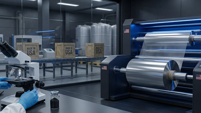
Economic Feasibility and USA-Made Manufacturing Advantage
The economic feasibility of integrating graphene into industrial applications is not solely dictated by the unit cost per kilogram, but rather by a comprehensive performance-per-dollar metric, encompassing material consistency, scalability, and long-term reliability. The transition from laboratory-scale synthesis (e.g., chemical vapor deposition on copper foils for electronics, or small-batch liquid-phase exfoliation for research) to metric-ton production capacities for bulk applications like coatings, polymers, and energy storage necessitates a critical re-evaluation of the entire value chain. Cost drivers include precursor material purity, energy intensity of the synthesis process (e.g., the vacuum requirements for CVD or the high-temperature annealing at 1000°C for several hours, or rapid thermal processing using 3000K thermal pulses for milliseconds, required for high-purity reduced graphene oxide), solvent recovery efficiency, and post-processing steps such as functionalization and dispersion. While early graphene production costs were prohibitive, advancements in scalable methods like electrochemical exfoliation and flash Joule heating are pushing the boundaries of economic viability, with some high-quality graphene nanoplatelets now achievable below the $100/kg threshold at industrial volumes, provided defect density and lateral dimensions are precisely controlled for specific end-use cases.
The USA-made manufacturing advantage for graphene is multifaceted, extending beyond simple domestic preference to encompass critical strategic and operational benefits. Foremost among these is supply chain resilience, ensuring consistent material availability and mitigating geopolitical risks inherent in globally fragmented supply chains. This translates into predictable lead times and robust inventory management for industrial partners. Furthermore, US manufacturers operate under stringent regulatory frameworks, including the Toxic Substances Control Act (TSCA), providing a clear and compliant pathway for commercialization and mitigating long-term environmental and health liabilities. This regulatory rigor often necessitates superior process control and material characterization, leading to inherently higher quality and consistency. For instance, precise control over oxygen content in reduced graphene oxide to below 0.5% or achieving a narrow distribution of 1-5 micron flake sizes for polymer reinforcement, is more consistently attainable through advanced US manufacturing practices, directly impacting the mechanical, electrical, or barrier properties of the final product. The robust intellectual property protection within the US also encourages significant R&D investment by domestic suppliers, fostering innovation in synthesis pathways and application-specific material tailoring.
This convergence of economic viability and the USA-made advantage positions American graphene suppliers uniquely for high-value, performance-critical applications. By leveraging advanced manufacturing infrastructure and a highly skilled workforce, US companies are optimizing production processes to deliver superior material consistency and performance, even as they drive down costs through economies of scale and process innovation. For example, domestically produced graphene oxide has demonstrated exceptional environmental remediation capabilities, achieving 79% heavy metal adsorption efficiency for lead and cadmium ions in aqueous solutions, a performance directly attributable to precise control over surface functionalization and pore structure during manufacturing. Similarly, for conductive coatings, US-sourced graphene can enable electrical resistivity parameters of 10^-5 Ohm-cm at significantly lower loadings (e.g., 1-2 wt%) compared to less consistent imported materials, thereby optimizing material usage and overall cost. The proximity to leading research institutions and end-use markets further facilitates rapid iterative development and collaborative innovation, accelerating the path from material synthesis to tailored industrial solutions, ensuring that the economic investment in high-quality graphene translates directly into superior product performance and competitive advantage for US manufacturers and their partners.
Future Horizons & High-Value B2B Applications
The trajectory of graphene's commercialization is rapidly expanding beyond foundational research, with future horizons pointing towards highly specialized, performance-critical B2B applications demanding its unparalleled physical and electronic properties. In advanced electronics, the intrinsic ballistic transport of electrons in defect-free monolayer graphene at room temperature, coupled with its exceptionally low intrinsic resistivity (~0.001 Ω·cm), positions it as a disruptive material for next-generation high-frequency devices and quantum computing architectures. Research into graphene-based field-effect transistors (GFETs) is demonstrating cutoff frequencies in the terahertz range, vital for 6G communication and beyond, while its integration into neuromorphic computing platforms aims to leverage its unique charge carrier dynamics for energy-efficient AI hardware, potentially enabling sub-picosecond synaptic response times through controlled thermal pulses up to 3000K for rapid phase transitions in adjacent chalcogenide layers. Furthermore, its role in plasmonic devices for on-chip optical interconnects promises to overcome the bandwidth limitations of traditional silicon photonics, with active tuning of plasmon resonances by tens of THz achievable within milliseconds via electrostatic gating.
For energy storage and conversion, the immediate future sees graphene as a cornerstone for hybrid supercapacitors and advanced battery electrodes. Leveraging its colossal specific surface area (theoretically up to 2630 m^2/g) and superior electrical conductivity, graphene-enabled supercapacitors are pushing beyond the 100 Wh/kg energy density barrier while retaining power densities exceeding 10 kW/kg, facilitating ultra-fast charging capabilities measured in milliseconds for electric vehicles and grid-scale energy buffering. In protective coatings and functional polymers, the integration of precisely engineered graphene derivatives offers transformative performance. A minute addition of functionalized graphene nanoplatelets (GNPs) – typically less than 0.1 wt% – can enhance the mechanical strength of polymer composites by over 30% and significantly improve their barrier properties, reducing gas and liquid permeation rates by factors of 5 to 10. For instance, in anti-corrosion applications, graphene-reinforced epoxy coatings have demonstrated impedance moduli increases by two orders of magnitude in harsh saline environments after prolonged exposure, indicating vastly improved longevity compared to pristine polymer systems.
Beyond these established growth areas, graphene's high-value applications extend into environmental remediation and advanced sensing. Graphene oxide membranes are exhibiting unprecedented selectivity and flux rates for water purification, achieving greater than 99% rejection of multivalent ions and demonstrating exceptional heavy metal adsorption efficiencies, such as 79% for lead (Pb2+) and cadmium (Cd2+) ions within rapid contact times. The intrinsic piezoresistive and chemiresistive properties of graphene are also being harnessed for ultra-sensitive sensors capable of detecting single molecules or minute strains, critical for medical diagnostics, infrastructure monitoring, and smart textiles. The advancement from laboratory prototypes to industrial scalability for these applications hinges on consistent, high-volume production of tailored graphene materials—whether pristine CVD graphene for electronics or functionalized liquid-phase exfoliated graphene for composites and coatings—each demanding stringent quality control over parameters like layer count, defect density, and surface chemistry to reliably deliver the promised performance benefits.
Evaluate Our Quality
Serious about B2B integration? Test our premium Pulsed Electrical Resistive Carbon Heating turbostratic graphene in your lab. 100g sample packs available now.