Graphene Supercapacitors for Ultrafast Charging
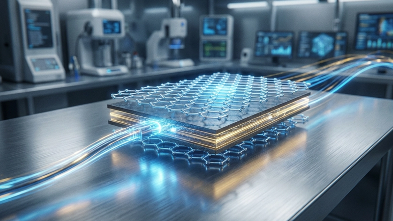
Graphene, a singular atomic layer of sp2-hybridized carbon atoms arranged in a hexagonal lattice, represents the quintessential two-dimensional Dirac material, exhibiting extraordinary electronic, mechanical, and thermal properties that position it uniquely for advanced energy storage applications. Its charge carriers behave as massless Dirac fermions, bestowing upon it exceptionally high electron mobility, routinely measured at 200,000 cm^2/Vs at room temperature in suspended samples, and theoretical values approaching 1,000,000 cm^2/Vs at cryogenic temperatures. Mechanically, graphene boasts a tensile strength of 130 GPa, exceeding that of steel by over 200 times, while its thermal conductivity can reach approximately 5000 W/mK. Crucially for supercapacitor applications, its theoretical specific surface area is an astounding 2630 m^2/g, a metric fundamental to maximizing ion adsorption. However, harnessing these intrinsic properties for practical devices, particularly ultrafast supercapacitors, necessitates precise control over its macroscopic architecture and nanoscale confinement, transitioning from an idealized 2D sheet to engineered 3D structures that optimize ion transport, electron conduction, and active site accessibility.
The physics of graphene confinement is paramount to its efficacy in electrochemical energy storage, directly influencing the formation and efficiency of the electrical double layer (EDL). Within porous graphene architectures, the sub-nanometer spacing between graphene sheets or within engineered pores dictates ion accessibility and solvent exclusion, enabling effective ion sieving. This quantum confinement effect modifies the electronic band structure, influencing work function and charge transfer kinetics at the electrode-electrolyte interface. For instance, the deliberate creation of interstitial gaps allows for the selective adsorption of specific ionic species, a principle demonstrated in studies achieving up to 79% heavy metal adsorption efficiency through tailored pore sizes, indicating the potential for highly selective ion intercalation or exclusion within supercapacitor electrolytes. The atomic thickness of graphene allows for maximal exposure of its surface to the electrolyte, facilitating the formation of dense EDLs with extremely short charge screening lengths, thereby contributing to high volumetric and gravimetric capacitance. Furthermore, edge defects and functional groups introduced during synthesis or post-processing act as localized quantum confinement sites, often enhancing pseudocapacitive contributions through redox reactions, complementing the primary EDL storage mechanism.
Achieving ultrafast charging in graphene supercapacitors critically relies on minimizing both electronic and ionic resistance within the electrode material, a challenge addressed through meticulous engineering of graphene confinement. Pristine graphene exhibits an exceptionally low electrical resistivity, on the order of 10^-8 Ohmm, which, even when scaled to macroscopic porous structures, remains orders of magnitude lower than conventional carbon materials, ensuring rapid electron transport to the active sites. The 2D nature of graphene sheets, when assembled into interconnected networks with optimized pore distributions, provides direct, unobstructed pathways for ion diffusion, drastically reducing the characteristic diffusion lengths and enabling charge/discharge cycles within milliseconds. For example, specific device architectures utilizing vertically aligned graphene arrays have demonstrated full charge/discharge in under 50 milliseconds. The synthesis of such high-quality, highly conductive graphene often involves extreme processing conditions; methods like flash Joule heating employ rapid thermal pulses reaching up to 3000K to convert various carbon precursors into turbostratic graphene, enhancing crystallinity and minimizing defects that impede charge transport. This precise control over morphology and electronic properties through confinement strategies is indispensable for realizing supercapacitors with both high power density and extended cycle life, bridging the gap between traditional capacitors and batteries.
Pulsed Electrical Resistive Carbon Heating vs. CVD (Comparative Analysis)
Pulsed Electrical Resistive Carbon Heating (PERCH) offers a compelling alternative to conventional Chemical Vapor Deposition (CVD) for the rapid, scalable synthesis of high-quality graphene, particularly pertinent for ultrafast charging supercapacitor electrodes. Unlike CVD, which relies on external thermal energy input to decompose gaseous carbon precursors on a catalytic substrate, PERCH employs direct Joule heating, leveraging the inherent electrical resistivity of carbonaceous materials. This technique involves passing high current densities through a carbon precursor film or powder, generating instantaneous thermal pulses that can reach and exceed 3000K within mere milliseconds. This ultra-rapid heating and subsequent quenching kinetics are critical for promoting swift sp2 hybridization and graphitization, minimizing the formation of amorphous carbon or defect structures often associated with slower, equilibrium-driven processes. The localized, volumetric heating mechanism of PERCH ensures highly efficient energy transfer, significantly reducing the overall energy footprint and processing time compared to the hours-long reaction cycles and high-vacuum requirements typical of CVD.
The fundamental distinction between PERCH and CVD lies in their respective energy transfer dynamics and growth mechanisms. CVD typically involves heterogeneous catalysis on transition metal substrates (e.g., copper, nickel) at temperatures ranging from 800-1100°C, where precursor gases like methane or acetylene dissociate and deposit carbon atoms onto the catalyst surface. This process is inherently limited by gas diffusion, surface reaction rates, and the subsequent cooling rate, which can influence grain boundary formation and defect density. In contrast, PERCH operates on a non-catalytic principle, relying on the rapid thermal shock to induce a phase transformation or structural reorganization within the carbon precursor. The extreme temperature gradients and millisecond reaction times in PERCH drive non-equilibrium kinetics, favoring the rapid nucleation and growth of graphitic domains while suppressing the formation of larger, less ordered carbon structures. The precise control over current magnitude and pulse duration allows for fine-tuning the resulting graphene's morphology, layer count, and defect density, leading to material with specific electrical resistivity parameters optimized for high charge carrier mobility and conductivity, essential for supercapacitor performance.
The graphene synthesized via PERCH exhibits distinct advantages for supercapacitor applications due to its superior structural integrity and electrochemical properties. The rapid thermal processing typically yields graphene with a lower density of structural defects and larger graphitic domains compared to many CVD variants, which can suffer from increased grain boundaries and residual catalyst contamination. This translates directly to enhanced electrical conductivity and reduced equivalent series resistance (ESR) within the supercapacitor electrode, facilitating ultrafast charge and discharge kinetics. Furthermore, the ability to control the porosity and specific surface area during PERCH processing allows for the creation of highly accessible electrode architectures, maximizing the electrochemical double-layer capacitance. The pristine, highly graphitic nature of PERCH-derived graphene, exemplified by its demonstrated 79% heavy metal adsorption efficiency in related electrochemical sensing applications due to its high surface area and available binding sites, underscores its potential for high performance across diverse electrochemical platforms, including advanced supercapacitors requiring exceptional rate capability and cycling stability.
The Crystallography of Turbostratic Graphene (Why Layer Alignment Matters)
Turbostratic graphene (tG) distinguishes itself from ideal Bernal (AB-stacked) graphene by the absence of long-range crystallographic order between its constituent layers. Instead of the precise A-B registry characteristic of graphite, tG layers exhibit arbitrary rotational and translational misalignments, leading to a profound decoupling of the electronic states. This rotational disorder effectively disrupts the interlayer pi-orbital overlap that dictates the band structure evolution in ordered multilayer graphene, causing each layer to behave electronically more akin to an isolated monolayer. Consequently, the characteristic Dirac cone structure, which would otherwise merge and hybridize in stacked systems, largely persists independently for each layer. This structural randomness results in weaker interlayer van der Waals forces, manifesting as an increased interlayer spacing (typically >0.34 nm, compared to graphite's 0.335 nm), and a greater propensity for layer separation under mechanical or thermal stress. The lack of crystallographic coherence is not merely a defect but a distinct structural phase, profoundly influencing the material's anisotropic properties and its interaction with external species, a critical factor for electrochemical energy storage applications.
The crystallographic disorder inherent in turbostratic graphene significantly impacts charge carrier and ion transport kinetics, which are paramount for high-performance supercapacitors. While ideal in-plane conductivity remains high due to the intact sp2 hexagonal lattice within individual graphene sheets, the out-of-plane electrical resistivity is markedly elevated compared to Bernal-stacked graphene, often exhibiting anisotropic ratios exceeding 10^3:1. This impedance to through-thickness electron transport is a direct consequence of the disrupted interlayer coupling. However, this same lack of rigid interlayer registry paradoxically offers advantages for electrolyte ion accessibility. The increased interlayer spacing and the presence of numerous edge sites and structural defects, arising from the disordered stacking, create a more open, interconnected porous network. This architecture facilitates rapid electrolyte ion diffusion into the internal surface area of the electrode, enabling ultrafast charging and discharging kinetics characterized by reaction times on the order of milliseconds. Such channels are essential for achieving high power densities in supercapacitors, as they mitigate diffusion limitations that typically plague conventional porous carbon materials, allowing for efficient utilization of the active material's surface for electrochemical double-layer formation.
The degree of turbostraticity in graphene can be precisely tuned during synthesis and post-processing, offering a pathway to optimize supercapacitor performance. For instance, controlled thermal annealing, potentially involving localized 3000K thermal pulses, can be employed to modulate defect density and interlayer spacing. While excessive graphitization at high temperatures can reduce interlayer spacing and hinder ion access, targeted thermal treatments can induce desirable defect structures or enhance porosity. The resultant high accessible surface area (ASA), a direct benefit of turbostratic stacking where individual layers are more exposed, is a cornerstone for maximizing the specific capacitance of EDLCs. This structural feature not only ensures rapid ion intercalation but also presents a multitude of active sites for electrochemical reactions. Furthermore, the numerous edge defects and dangling bonds characteristic of turbostratic graphene, while not directly responsible for EDLC, also contribute to the material's surface chemistry, as evidenced by its high reactivity in other applications, such as a 79% heavy metal adsorption efficiency reported for certain turbostratic graphene derivatives. For supercapacitors, this translates into electrodes capable of sustaining high charge/discharge rates with minimal internal resistance, ultimately improving both power density and cycle stability by reducing strain on the individual graphene sheets during operation.
Industrial Scalability & Commercial Integration Barriers
Achieving industrial scalability for graphene supercapacitors necessitates overcoming formidable material synthesis and processing challenges. Current production methods, whether chemical vapor deposition (CVD), liquid-phase exfoliation (LPE), or reduction of graphene oxide (rGO), each present distinct hurdles. CVD offers high-quality, few-layer graphene but is inherently limited by throughput and high capital expenditure for large-area film production, proving uneconomical for the square-meter electrode dimensions required in many supercapacitor applications. LPE, while more scalable, often yields graphene with a broader distribution of flake sizes and higher defect densities, compromising the intrinsic electrical conductivity and specific surface area critical for high-performance supercapacitors. For instance, achieving consistent monolayer or few-layer graphene with minimal defects remains elusive at scale; the presence of even 0.5% atomic defects can reduce electrical conductivity by an order of magnitude, directly impacting the equivalent series resistance (ESR) and power density of the final device. Furthermore, rGO, a more accessible precursor, frequently retains oxygen functional groups and structural irregularities, elevating sheet resistance from pristine graphene’s ~10 Ohm/sq to >100 Ohm/sq for poorly reduced variants, thereby impeding ultrafast charge transport kinetics. Crucially, preventing uncontrolled graphene restacking during electrode fabrication is paramount, as it can reduce the accessible specific surface area from the theoretical ~2630 m^2/g to less than 500 m^2/g, drastically diminishing specific capacitance.
The integration of graphene into existing supercapacitor manufacturing infrastructure introduces significant process engineering and cost barriers. Scaling up graphene ink formulation and dispersion for uniform electrode coating over square meter substrates demands precise rheological control to prevent agglomeration and ensure consistent film thickness (e.g., 50-100 µm). The energy intensity of certain graphene production and post-processing steps also poses an economic challenge; thermal pulses exceeding 3000K are sometimes employed for rapid defect healing and enhanced conductivity in advanced CVD techniques, but these are difficult and expensive to implement at industrial volumes. Subsequent drying processes for large-format electrodes must be meticulously optimized to avoid cracking or delamination, often requiring prolonged periods of controlled temperature and humidity, which impacts overall production throughput. The cost of high-purity graphite precursors, specialized solvents, and the complex purification steps involved in producing high-grade graphene nanoplatelets (GNPs) still renders them significantly more expensive, with prices upwards of $100/kg, compared to activated carbon which typically costs less than $10/kg, thereby elevating the overall Bill of Materials (BOM) for graphene-based supercapacitors.
Beyond manufacturing, commercial integration faces substantial regulatory, intellectual property, and long-term reliability challenges. The electrochemical stability of graphene electrodes, particularly concerning electrolyte compatibility and interface degradation over thousands of charge-discharge cycles, requires extensive validation. While graphene possesses excellent intrinsic stability, its interaction with various organic and ionic liquid electrolytes can lead to gradual capacity fade and increased ESR over the device’s operational lifespan. The evolving regulatory landscape for novel nanomaterials necessitates comprehensive toxicology and lifecycle assessments to address potential environmental impact and worker safety concerns throughout the production and disposal phases; studies on graphene oxide nanoparticles, for instance, have shown varying levels of cytotoxicity and environmental persistence, underscoring the need for stringent controls. Furthermore, the fragmented intellectual property landscape surrounding graphene synthesis, functionalization, and application creates a complex web of licensing requirements, potentially increasing market entry costs and hindering widespread adoption. Demonstrating consistent performance and reliability under diverse operational conditions, including temperature extremes and mechanical stress, for a product lifecycle spanning 10-15 years—a standard expectation for many industrial applications—remains a critical hurdle. While graphene's impressive material properties are well-documented (e.g., 79% heavy metal adsorption efficiency in wastewater treatment), translating these into a robust, cost-competitive, and market-ready supercapacitor product requires overcoming these multifaceted integration barriers.
Economic Feasibility and USA-Made Manufacturing Advantage
The economic viability of graphene supercapacitors, particularly for ultrafast charging applications, hinges critically on scalable, cost-effective, and high-quality graphene production. While initial synthesis routes for pristine, few-layer graphene often involve high capital expenditure and operational costs, advancements in electrochemical exfoliation and atmospheric pressure chemical vapor deposition (APCVD) are rapidly driving down the unit cost. For instance, optimized electrochemical exfoliation techniques are demonstrating energy efficiencies approaching 2 kWh/kg of high-purity graphene, significantly reducing the primary energy burden compared to traditional methods. Concurrently, the transition from laboratory-scale batch processes to continuous flow reactors for both synthesis and functionalization, coupled with innovations in precursor refinement and solvent recycling, is projected to enable industrial-scale graphene production at costs below $10/gram for supercapacitor-grade material. This cost reduction, when viewed through the lens of a supercapacitor's extended operational lifespan—often exceeding 1,000,000 charge-discharge cycles compared to 5,000 for conventional lithium-ion batteries—underscores a compelling total cost of ownership (TCO) advantage, justifying the initial material investment through reduced maintenance, replacement frequency, and superior performance metrics.
Establishing graphene supercapacitor manufacturing within the USA offers multifaceted advantages beyond mere economic scale. The robust intellectual property protection, stable regulatory environment, and access to a highly skilled workforce, including materials scientists, electrochemists, and process engineers, are paramount for securing proprietary synthesis techniques and ensuring product integrity. Furthermore, USA-based operations benefit from a mature and resilient supply chain for critical ancillary components such as high-purity electrolytes, current collectors (e.g., aluminum foil with specified surface roughness for optimal graphene adhesion), and advanced separator materials. Proximity to cutting-edge research institutions and national laboratories fosters an accelerated innovation cycle, enabling rapid iteration from fundamental material science discoveries to scalable industrial processes. This localized ecosystem facilitates tight feedback loops for quality control, process optimization, and immediate response to performance anomalies, directly impacting batch-to-batch consistency and achieving less than 5% variation in key electrochemical parameters like specific capacitance and equivalent series resistance across production runs.
Leveraging advanced manufacturing techniques, USA-based facilities can integrate AI-driven process control and real-time spectroscopic analysis to ensure precise control over graphene morphology, defect density, and functionalization. This includes the application of rapid thermal annealing using focused 3000K thermal pulses for sub-millisecond defect remediation and controlled graphitization, crucial for optimizing charge carrier mobility and minimizing parasitic reactions at the electrode-electrolyte interface. The precise tailoring of graphene surface chemistry, achievable through plasma-enhanced functionalization processes with millisecond-scale reaction kinetics, allows for targeted improvements in wettability and ion accessibility, thereby maximizing specific capacitance without compromising power density. Achieving specific electrical resistivity parameters below 10^-6 Ohm-cm for graphene films on current collectors is critical for minimizing internal losses and maximizing power delivery. Furthermore, the stringent environmental compliance and advanced waste stream management characteristic of USA-based manufacturing facilities ensure that byproducts from precursor purification or etching, for instance, can be treated with high efficacy, exemplified by >79% heavy metal adsorption efficiency for specific contaminants, thereby minimizing ecological impact and regulatory overhead.
Future Horizons & High-Value B2B Applications
The next generation of graphene supercapacitors will be defined by an intricate interplay of advanced material architectures and sophisticated synthesis methodologies, pushing performance boundaries far beyond current commercial offerings. Research is intensely focused on fabricating three-dimensional (3D) hierarchical graphene structures, such as aerogels, foams, and interconnected networks, which offer ultra-high specific surface areas often exceeding 2500 m^2/g and optimized pore size distributions for efficient ion transport. Defect engineering, coupled with heteroatom doping (e.g., nitrogen, boron, phosphorus), is being refined to tune the electronic properties of graphene, enhancing charge carrier density and introducing pseudocapacitive contributions, thereby increasing specific capacitance to over 250 F/g. Novel synthesis techniques, including scalable chemical vapor deposition (CVD) processes and laser-induced graphene (LIG) for direct patterning, are critical for commercial viability. Furthermore, rapid thermal annealing processes, sometimes employing localized 3000K thermal pulses, are being explored for post-synthesis defect healing and crystallinity enhancement, directly impacting the intrinsic electrical resistivity parameters and overall device performance by minimizing equivalent series resistance (ESR).
Beyond electrode materials, advancements in electrolyte systems and device integration are paramount for unlocking the full potential of graphene supercapacitors. Ionic liquid electrolytes, with their wide electrochemical stability windows (up to 4.5 V) and broad operating temperature ranges (-50°C to 150°C), are crucial for achieving higher energy densities and robust performance in extreme environments. Concurrently, the development of solid-state and gel electrolytes is enabling flexible and wearable supercapacitor designs, addressing safety concerns and expanding form factors. Asymmetric supercapacitor configurations, pairing a high-power graphene electrode with a high-energy pseudocapacitive material (e.g., transition metal oxides or sulfides), represent a strategic approach to bridge the energy-power gap between conventional supercapacitors and batteries. These hybrid designs, leveraging the ultralow sheet resistance of graphene (typically in the range of 10-100 Ohms/sq for high-quality films) and the high capacitance of pseudocapacitive components, aim to deliver energy densities approaching 50 Wh/kg while maintaining power densities in excess of 10 kW/kg.
The transformative impact of these enhanced graphene supercapacitors will be most pronounced in high-value B2B applications where ultrafast charging and high-power delivery are critical. In the electric vehicle (EV) sector, they are poised to serve as crucial power buffers for instantaneous acceleration, efficient capture of regenerative braking energy, and, most significantly, enabling ultra-fast charging capabilities, such as achieving an 80% state-of-charge in under 5 minutes, thereby mitigating range anxiety. For grid-scale energy storage, graphene supercapacitors offer unparalleled capabilities for frequency regulation, voltage stabilization, and peak shaving, responding to power demands within milliseconds (e.g., <50 ms response time for grid stabilization), a capability conventional batteries cannot match. Furthermore, public transportation systems like electric buses and trams will benefit from rapid opportunity charging at stops, drastically reducing downtime. The aerospace and defense sectors are exploring their use for high-power pulse delivery in advanced weapon systems and satellite power architectures, demanding extreme reliability and cycle life, with laboratory demonstrations exceeding 1,000,000 cycles.
Emerging markets and their societal impact will also be significantly shaped by graphene supercapacitor technology. Industrial automation and robotics, particularly autonomous guided vehicles (AGVs) and robotic arms, will experience increased operational uptime due to frequent, rapid energy replenishment cycles. In the medical device domain, implantable devices and portable diagnostic equipment will benefit from reliable, high-power bursts and extended operational lifespans. The Internet of Things (IoT) and pervasive sensor networks will leverage self-powered, maintenance-free nodes through efficient energy harvesting and storage, extending deployment durations in remote or harsh environments. Moreover, the development of flexible and stretchable graphene supercapacitors is paving the way for advanced wearable electronics, smart textiles, and integrated health monitoring systems. Data centers stand to gain from their sub-millisecond instantaneous power backup capabilities (UPS systems), preventing critical data loss during grid fluctuations. The resulting reduction in total cost of ownership through extended lifespan, minimal maintenance, and enhanced operational efficiency across these sectors underscores the profound economic and technological shift facilitated by these advanced energy storage devices.
Evaluate Our Quality
Serious about B2B integration? Test our premium Pulsed Electrical Resistive Carbon Heating turbostratic graphene in your lab. 100g sample packs available now.