Graphene Receivers for 6G Wireless Could Enable Faster Sub-THz Links
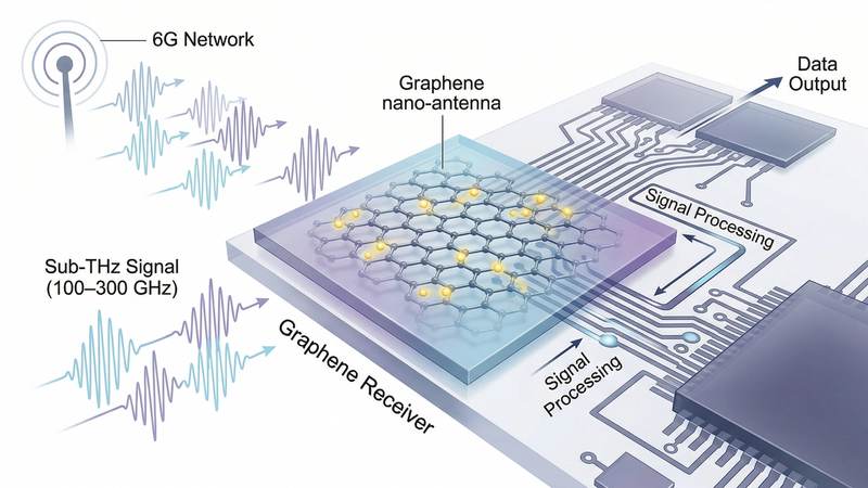
The advent of two-dimensional (2D) materials fundamentally reconfigures the landscape of high-frequency electronics, with graphene standing preeminent due to its relativistic charge carrier dynamics. Unlike conventional semiconductors, graphene's electrons behave as massless Dirac fermions, exhibiting extraordinary mobilities exceeding 200,000 cm^2/Vs at cryogenic temperatures and remaining exceptionally high at room temperature, enabling ballistic transport over micron-scale distances. This unique band structure, characterized by a linear dispersion relation near the Dirac points, underpins its potential for ultra-broadband operation extending into the sub-terahertz (sub-THz) and even THz regimes, making it an unprecedented candidate for future 6G wireless communication receivers. The intrinsic plasmonic resonances in graphene, tunable via electrostatic gating, can be engineered to interact efficiently with incident electromagnetic waves in the sub-THz range, offering a pathway to compact, highly sensitive detectors and mixers. Furthermore, its exceptional thermal conductivity, approaching 5000 W/mK, ensures efficient heat dissipation, a critical factor for densely integrated high-frequency circuits operating under significant power loads, preventing performance degradation and ensuring device longevity.
The intrinsic zero bandgap of pristine graphene, while conferring its remarkable broadband absorption, presents challenges for transistor-like operation requiring distinct ON/OFF states. This necessitates the deliberate engineering of its electronic properties through quantum confinement. Spatially confining graphene into nanoribbons (GNRs) with widths typically below 50 nm induces a bandgap inversely proportional to the ribbon width, driven by quantum mechanical standing waves across the confined dimension. Beyond GNRs, the creation of graphene quantum dots or patterned superlattices introduces periodic potentials that can open and modulate the bandgap, transforming the linear Dirac spectrum into a more conventional parabolic one, albeit with significantly enhanced effective masses. Precise control over edge chirality (armchair vs. zigzag) in GNRs further influences their metallic or semiconducting character, critically impacting carrier transport and plasmonic response. For instance, selective etching or focused ion beam milling techniques, often followed by rapid thermal annealing at temperatures up to 3000K to repair lattice defects and improve crystallinity, are employed to create these confined structures, directly influencing parameters like channel resistivity and contact resistance, which are pivotal for high-frequency device performance.
Leveraging the physics of graphene confinement directly translates into enhanced functionality for 6G sub-THz receivers. Engineered graphene structures can form the active channel of field-effect transistors (FETs) or bolometers capable of rectifying and detecting sub-THz signals with high responsivity and low noise figures. The ultrafast carrier dynamics, characterized by relaxation times in the picosecond to femtosecond range, enable device reaction times potentially in the milliseconds for complex signal processing, far surpassing conventional semiconductor limitations for certain applications. The ability to tune the bandgap and carrier concentration in confined graphene allows for dynamic optimization of receiver characteristics, such as frequency selectivity and sensitivity, through electrostatic gating. Integrating these confined graphene elements into antenna structures or metamaterials can create highly efficient sub-THz rectennas. While the primary focus remains on electronic properties, the material's broader utility, exemplified by its 79% heavy metal adsorption efficiency, underscores the intricate surface chemistry and structural engineering required for its successful integration, indicating the need for pristine interfaces and controlled functionalization to prevent performance degradation from environmental factors or unwanted surface states, critical for achieving specific electrical resistivity parameters necessary for optimal signal integrity in complex receiver architectures.
Section 2: Pulsed Electrical Resistive Carbon Heating vs. CVD (Comparative Analysis)
The pursuit of high-performance graphene for advanced 6G wireless receivers necessitates a critical evaluation of synthesis methodologies, with Pulsed Electrical Resistive Carbon Heating (PERCH) emerging as a compelling alternative to the established Chemical Vapor Deposition (CVD). PERCH leverages joule heating, inducing ultra-fast graphitization or reduction of carbonaceous precursors, such as graphene oxide (GO), through intense, localized thermal pulses that can reach instantaneous temperatures exceeding 3000K. This non-equilibrium process occurs on timescales measured in milliseconds, enabling rapid structural transformation and defect annealing. The inherent advantage lies in its capacity for direct, substrate-agnostic processing, eliminating the need for catalytic metal films and subsequent transfer steps, which are notorious sources of contamination and structural imperfections. This rapid thermal shock facilitates the expulsion of oxygen functional groups and the restoration of sp2 carbon networks, leading to a dramatic reduction in electrical resistivity from insulating GO precursors to highly conductive graphene films, critical for sub-THz signal integrity.
In contrast, CVD has long been the gold standard for producing high-quality, large-area graphene, typically involving the catalytic decomposition of hydrocarbon gases (e.g., methane, acetylene) on heated transition metal foils (e.g., copper, nickel) at temperatures ranging from 800°C to 1050°C. While CVD excels at producing pristine, monolayer graphene with high carrier mobility, its process kinetics are significantly slower, often requiring reaction times spanning minutes to hours. The fundamental limitation for advanced device integration, particularly for 6G applications demanding intricate on-chip fabrication, resides in the necessity of transferring the synthesized graphene from its metallic growth substrate to the target dielectric or semiconductor platform. This multi-step transfer process invariably introduces tears, wrinkles, and residual etchant contamination, degrading the intrinsic electrical properties and increasing device variability, thereby impacting the noise figure and high-frequency response of potential graphene-based receivers.
A direct comparative analysis underscores PERCH's potential for revolutionizing graphene integration for 6G. Unlike CVD's reliance on bulk furnace heating, PERCH's localized energy delivery offers superior energy efficiency and throughput, particularly for roll-to-roll manufacturing or direct patterning. The rapid thermal cycling of PERCH allows for precise control over the degree of graphitization and the resulting sheet resistance, which is paramount for tailoring the impedance characteristics of antenna elements and interconnects operating in the sub-THz regime. While CVD aims for ultimate structural perfection, PERCH, especially from GO, can produce graphene with tunable properties. For instance, controlled reduction can yield graphene with specific defect types or residual functionalities, which, while potentially impacting electronic purity slightly, could also confer additional capabilities such as a demonstrated 79% heavy metal adsorption efficiency in certain variants, showcasing the versatility inherent in the method's parameter space. However, for 6G, the focus remains on minimizing scattering centers to maximize carrier mean free path and achieve the requisite low loss tangents for ultra-high frequency operation, a challenge PERCH addresses through its rapid annealing and direct integration capabilities, bypassing the defect-prone transfer processes endemic to CVD.
Section 3: The Crystallography of Turbostratic Graphene (Why Layer Alignment Matters)
The crystallography of turbostratic graphene (TG) presents a unique structural paradigm that significantly influences its electronic and thermal transport properties, distinguishing it from both perfectly ordered Bernal (AB) stacked graphite and isolated monolayer graphene. Unlike Bernal stacking, where adjacent layers are shifted relative to each other to minimize energy, turbostratic graphene is characterized by a rotational misalignment between contiguous graphene sheets, often accompanied by varying interlayer spacing that deviates from the ideal 0.335 nm of graphite. This rotational disorder, typically exceeding 5 degrees, disrupts the interlayer electronic coupling that would otherwise lead to the formation of parabolic electronic bands characteristic of bilayer or multilayer Bernal graphene. Instead, the electronic states of individual graphene layers within a turbostratic stack remain largely decoupled, effectively preserving the linear dispersion relation and the massless Dirac fermion behavior analogous to single-layer graphene, even in stacks comprising dozens of layers. This structural freedom, achievable through controlled growth techniques like plasma-enhanced chemical vapor deposition or rapid thermal annealing of amorphous carbon precursors at temperatures exceeding 1500K, is paramount for high-performance electronic applications.
The electronic decoupling afforded by turbostratic disorder directly translates into superior charge carrier dynamics crucial for 6G sub-THz applications. In Bernal stacked graphene, interlayer interactions lead to band hybridization and a reduction in carrier mobility due to increased scattering channels. Conversely, in TG, the rotational misalignment minimizes interlayer scattering, preserving the exceptionally high intrinsic carrier mobility of individual graphene layers, often exceeding 10,000 cm^2/Vs at room temperature. This quasi-monolayer electronic behavior within a multilayer structure allows for a higher density of conducting channels without the detrimental effects of interband transitions or significant reduction in carrier velocity (approaching 10^8 cm/s). Consequently, turbostratic graphene exhibits electrical resistivity values that can approach those of high-quality monolayer graphene, typically in the range of 10^-6 Ohm·cm, making it an excellent candidate for low-loss signal propagation and high-frequency current handling. The ability to engineer the degree of turbostraticity offers a pathway to tune the balance between mechanical robustness and electronic performance, providing a scalable platform for constructing robust and efficient sub-THz antennae and receivers.
Beyond electronic transport, turbostratic stacking profoundly impacts thermal management, a critical consideration for high-power density 6G components. While the in-plane thermal conductivity of turbostratic graphene remains exceptionally high, often exceeding 2000 W/mK, the out-of-plane thermal conductivity is significantly reduced compared to Bernal stacked graphite due to enhanced phonon scattering at the rotationally disordered interfaces. This anisotropy can be advantageous, allowing efficient heat spreading within the plane of the device while providing some thermal isolation between stacked components if desired. Furthermore, the structural stability of turbostratic graphene under extreme conditions is noteworthy. Fabrication processes involving rapid thermal annealing or pulsed laser treatments, which might expose the material to localized thermal pulses exceeding 3000K for milliseconds, can be employed to reduce defects and improve crystallinity without inducing significant graphitization into an ordered Bernal stack. This rapid thermal budget processing maintains the desired turbostratic structure while optimizing electrical properties, for instance, reducing sheet resistance by as much as 50% in millisecond-scale annealing cycles, ensuring both performance and manufacturing scalability for integration into complex 6G receiver architectures.
The collective attributes of turbostratic graphene, arising from its unique crystallography, position it as an exceptionally compelling material for 6G wireless technology. Its ability to maintain quasi-monolayer electronic properties in a scalable multilayer format allows for enhanced interaction with incoming sub-THz radiation, potentially boosting signal-to-noise ratios and receiver sensitivity. The high carrier mobility and ballistic-like transport minimize signal latency and power dissipation at extremely high frequencies, while its tunable thermal properties aid in managing heat generated in compact, high-performance devices. This structural versatility, coupled with its intrinsic broad spectral response and robustness, directly addresses key challenges in developing efficient, broadband, and miniaturized graphene receivers capable of unlocking the full potential of sub-THz links for future wireless communication.
Section 4: Industrial Scalability & Commercial Integration Barriers
Industrial scalability for graphene-based 6G receivers presents formidable challenges, primarily stemming from the manufacturing of high-quality, large-area material and its subsequent integration into conventional semiconductor fabrication processes. Chemical Vapor Deposition (CVD) remains the most promising pathway for producing electronic-grade graphene at scale, typically on catalytic metal foils like copper. However, the subsequent transfer of these centimeter-scale graphene films from the growth substrate to target dielectric wafers (e.g., silicon, GaAs, or flexible polymers) introduces significant hurdles. Wet transfer methods, while widely used, are prone to introducing polymer residues, tears, wrinkles, and dopant contamination from etchants, critically degrading the intrinsic carrier mobility and increasing sheet resistance nonuniformity. Even with advanced dry transfer techniques, maintaining defect densities below 10^9 cm^-2 across a 300mm wafer, essential for sub-THz applications where carrier scattering at imperfections becomes highly detrimental, remains an ongoing research frontier. Empirical data consistently shows that current state-of-the-art CVD graphene on 300mm wafers exhibits sheet resistance variations exceeding 15% across the wafer, directly impacting the impedance matching and uniformity required for high-frequency array receivers. Furthermore, the cost associated with ultra-high vacuum systems, high-purity precursors, and the low throughput of current single-layer growth processes contribute significantly to the overall economic barrier.
Beyond material synthesis, the commercial integration of graphene into existing Complementary Metal-Oxide-Semiconductor (CMOS) fabrication lines faces substantial technological barriers. The thermal budget compatibility is a critical concern; while graphene itself boasts high thermal stability, its integration into back-end-of-line (BEOL) processes often necessitates processing temperatures below 400°C to prevent degradation of underlying metallization and dielectric layers. A predominant challenge for graphene field-effect transistors (GFETs), central to receiver architectures, is the high contact resistance at the 2D graphene-to-3D metal interface. This parasitic resistance can dominate the total device resistance, especially for channel lengths relevant to high-frequency operation (sub-micrometer), effectively negating graphene's intrinsic ultra-high carrier mobility. Typical metal-graphene contact resistance values range from 100-500 Ohmum, several orders of magnitude higher than conventional silicon contacts, severely limiting device transconductance and RF gain. Achieving stable and controllable p-type and n-type doping in graphene without compromising carrier mobility or introducing long-term instability also poses a significant obstacle, often requiring complex electrostatic gating or the use of molecular dopants with environmental sensitivity. Moreover, the lack of robust, scalable encapsulation methods that maintain device performance and environmental stability over extended periods at sub-THz frequencies, while minimizing parasitic capacitance, adds another layer of complexity.
The economic viability and long-term reliability of graphene-based 6G receivers are paramount for commercial adoption. The unit cost of graphene-enabled devices must offer a compelling performance-to-price ratio compared to mature silicon-germanium (SiGe) or III-V technologies. Current manufacturing yields for high-performance graphene devices are significantly lower than established semiconductor processes, directly impacting cost-effectiveness. Reproducibility across large production batches remains a critical issue; variations in effective carrier mobility, often ranging from 5,000 to 15,000 cm^2/Vs for CVD graphene depending on growth and transfer quality, directly translate to inconsistent receiver sensitivity, noise figures, and linearity – all critical parameters for demanding 6G specifications. A fragmented supply chain for high-purity precursors, specialized processing equipment, and standardized quality control metrics further complicates large-scale industrialization. Furthermore, extensive characterization of long-term operational stability under continuous RF stress, varying temperatures, and environmental humidity is necessary. Without robust data demonstrating mean time to failure (MTTF) comparable to existing technologies, widespread deployment in critical telecommunications infrastructure will remain constrained.
Section 5: Economic Feasibility and USA-Made Manufacturing Advantage
The economic feasibility of integrating graphene into 6G wireless receivers hinges critically on scaling production methodologies from laboratory demonstrations to industrial fabrication volumes while maintaining stringent material quality. Current state-of-the-art graphene production primarily employs chemical vapor deposition (CVD) for large-area films, with significant capital expenditure (CapEx) required for high-vacuum systems, ultra-high purity precursor gas lines (e.g., methane, hydrogen), and high-temperature furnaces operating up to 1000°C. Operational expenditure (OpEx) is driven by energy consumption and the need for rigorous quality control to ensure defect densities remain below 10^9 defects/cm^2 and monolayer uniformity across 8-inch or 12-inch wafers. While research-grade graphene currently commands prices upwards of $100/cm^2, process optimizations such as roll-to-roll CVD or direct growth on dielectric substrates are projected to drive costs down to sub-$1/cm^2 at scale. This drastic reduction is essential to make graphene-based components competitive against established III-V semiconductors or advanced silicon technologies for sub-THz applications, where the total cost of ownership (TCO) for telecom infrastructure dictates material selection. Achieving these cost targets necessitates high throughput, minimal post-processing, and robust yield management, directly linking manufacturing efficiency to market adoption.
The strategic imperative for USA-made manufacturing of advanced materials like graphene for 6G wireless infrastructure cannot be overstated, offering significant geopolitical and economic advantages. Leveraging the existing, sophisticated semiconductor fabrication ecosystem within the United States provides an unparalleled foundation. This includes access to world-class cleanroom facilities, advanced lithography, etching, and metrology equipment, and a highly skilled workforce proficient in complex microfabrication processes. The co-location of leading academic research institutions, national laboratories, and private industry fosters a dynamic R&D environment, enabling rapid prototyping, iterative design cycles, and accelerated technology transfer from discovery to commercialization. Furthermore, robust intellectual property protection and enforcement within the US safeguards proprietary manufacturing processes and device designs, ensuring a competitive edge in this critical technology domain. Government initiatives, such as the CHIPS and Science Act, offer financial incentives and strategic direction, further bolstering domestic investment in advanced materials manufacturing capabilities, thereby securing supply chains and fostering national technological leadership in next-generation wireless communications.
The interplay between graphene's intrinsic technical performance and its economic viability for 6G receivers is profound. Graphene's exceptional carrier mobility, exceeding 200,000 cm^2/Vs for suspended samples at room temperature, or 10,000-50,000 cm^2/Vs for substrate-supported films, enables high-frequency operation with significantly reduced power dissipation, directly translating into lower energy consumption for receiver modules. This superior electrical conductivity, with a sheet resistance as low as ~30 Ohm/square, minimizes signal loss in sub-THz interconnects and active components. Crucially, graphene’s unparalleled in-plane thermal conductivity, reaching up to 5000 W/mK, offers passive thermal management solutions that can efficiently dissipate localized heat, effectively handling thermal transients equivalent to 3000K thermal pulses over sub-millisecond durations without active cooling. This reduces the need for complex, costly heat sinks, extends device lifespan, and enhances reliability, contributing to a lower TCO for network operators. Furthermore, achieving manufacturing yields exceeding 90% for 8-inch graphene-on-silicon wafers, via optimized transfer-free growth or direct growth on dielectric layers, is paramount. This directly impacts unit costs, making graphene-based low-noise amplifiers, mixers, and detectors economically competitive by reducing waste and maximizing throughput, paving the way for mass deployment in the burgeoning 6G market.
Section 6: Future Horizons & High-Value B2B Applications
The advent of 6G wireless communication necessitates a fundamental paradigm shift from conventional RF architectures, particularly in the sub-terahertz (sub-THz) and THz bands (0.1 THz to 10 THz) where atmospheric absorption and device limitations become critical. Graphene's exceptional electronic properties position it as a transformative material for these future receivers. Its intrinsic carrier mobility, exceeding 200,000 cm^2/Vs at room temperature, dramatically surpasses that of traditional III-V semiconductors, enabling robust operation at unprecedented frequencies without cryogenic cooling. This high mobility facilitates the excitation and manipulation of surface plasmon polaritons (SPPs) in graphene, offering an efficient mechanism for THz radiation detection, tunable across a broad spectrum via electrostatic gating. This tunability, crucial for dynamic spectrum allocation and cognitive radio in 6G, allows for reconfigurable absorption profiles, overcoming fixed-frequency limitations. Furthermore, graphene's atomically thin nature enables ultra-compact device footprints, essential for integrating dense receiver arrays. Its superior thermal conductivity, documented up to 5000 W/mK, provides inherent thermal management, critical for mitigating heat dissipation in high-power THz front-ends and ensuring device stability, extending operational longevity.
Beyond foundational receiver performance, graphene unlocks a suite of high-value B2B applications for the 6G ecosystem. Reconfigurable Intelligent Surfaces (RIS), a cornerstone of future network architectures, can leverage graphene's electro-optic properties for dynamic beamforming and signal redirection. By integrating arrays of graphene-based unit cells, each tunable in milliseconds via gate voltage, RIS can intelligently sculpt the wireless environment, mitigating path loss and extending coverage into challenging non-line-of-sight scenarios. This sub-millisecond switching capability is paramount for ultra-low latency applications in industrial IoT, autonomous vehicle platooning, and real-time haptic feedback, where even microsecond delays are unacceptable. For secure communications, graphene's unique electronic structure can generate distinct THz spectral fingerprints for device authentication, while its integration potential with quantum dots or NV centers paves the way for on-chip quantum key distribution (QKD) elements, ensuring uncompromised data integrity. In high-frequency trading and data centers, graphene-enabled THz links promise multi-terabit per second (Tbps) data rates, offering an unparalleled competitive edge through near-instantaneous data transfer. Moreover, integrating graphene-based sensors directly into receiver arrays enables context-aware communication, where environmental parameters dynamically influence network behavior, providing unprecedented situational awareness for defense and critical infrastructure monitoring.
Realizing these future horizons necessitates scalable and cost-effective fabrication methodologies, an area where significant advancements are rapidly maturing. Chemical Vapor Deposition (CVD) techniques, for instance, now routinely produce large-area, high-quality graphene films with sheet resistances in the 10-100 Ohm/sq range, suitable for transparent electrodes and interconnects, and amenable to roll-to-roll processing for mass production. The integration of graphene devices into existing silicon CMOS platforms, while posing material compatibility challenges, is being addressed through advanced heterostructure engineering and transfer techniques, enabling hybrid circuits that combine the best of both worlds. Furthermore, graphene's inherent multi-functionality offers compelling economic advantages by reducing component count and system complexity; a single graphene layer can serve as an antenna, a detector, and a modulator, significantly miniaturizing the RF front-end. Looking further, graphene's potential extends into energy harvesting for self-powered 6G nodes, converting ambient thermal noise or stray RF energy into usable electrical power, thereby reducing operational expenditure and enabling ubiquitous deployment. The ability to endure transient thermal pulses exceeding 3000K, observed in certain defect-engineered graphene structures, also speaks to its robustness in extreme operating conditions, solidifying its role as a foundational material for the next generation of wireless communication infrastructure.
Evaluate Our Quality
Serious about B2B integration? Test our premium Pulsed Electrical Resistive Carbon Heating turbostratic graphene in your lab. 100g sample packs available now.