Graphene Production from Chlorination of Metallocenes: A Novel Route
Graphene, the archetypal two-dimensional material, represents a singular instance of atomic confinement, where carbon atoms are arranged in a hexagonal lattice, leading to a unique electronic structure fundamentally governed by relativistic quantum mechanics. Its sp2 hybridized orbitals form a robust planar network, creating a system where electrons behave as massless Dirac fermions, exhibiting a linear dispersion relation near the K and K' Dirac points in the Brillouin zone. This extraordinary electronic confinement to a single atomic plane imbues graphene with unparalleled properties, distinguishing it from all other known materials. The Fermi velocity, approximately 10^6 m/s, dictates the carrier dynamics, resulting in ballistic transport over micron-scale distances even at ambient temperatures, a phenomenon rarely observed in condensed matter systems.
The profound implications of this 2D confinement are evident in graphene's exceptional charge transport and thermal properties. The absence of backscattering for charge carriers in pristine graphene, due to its unique pseudospin symmetry, contributes to its remarkably high room-temperature electron mobility, often exceeding 15,000 cm^2/Vs, and an intrinsic electrical resistivity that can approach values significantly below 10^-8 Ohm-m. Thermally, graphene exhibits a thermal conductivity that can surpass 3000 W/mK, making it the most efficient heat conductor known, a direct consequence of its strong covalent bonds and phonon confinement within the single-atom-thick lattice. This confluence of electronic and thermal superlatives stems directly from the quantum mechanical boundary conditions imposed by its atomic thickness, where out-of-plane vibrational modes are suppressed and in-plane modes are highly efficient. Preserving this atomic precision and electronic integrity during synthesis is paramount, as any structural defect or impurity acts as a scattering center, significantly degrading these intrinsic properties.
Achieving and maintaining the pristine two-dimensional quantum confinement of graphene on a macroscopic scale, while simultaneously controlling its morphology and electronic band structure, remains a formidable challenge for industrial applications. The inherent sensitivity of graphene's properties to its synthesis environment necessitates advanced methodologies capable of atomic-level precision. For instance, the rapid thermal annealing processes often employed to enhance crystallinity or remove defects in precursor materials, involving brief 3000K thermal pulses lasting only milliseconds, critically influence the resulting charge carrier mobility and structural order. Furthermore, the vast surface-to-volume ratio, a direct consequence of its 2D nature, makes graphene an exceptional candidate for surface-dominated applications, such as advanced filtration and sensing. Functionalized graphene derivatives, for example, have demonstrated heavy metal adsorption efficiencies up to 79% for specific contaminants like Pb(II) in aqueous solutions, highlighting the crucial role of defect-free basal planes and precisely controlled surface chemistry. These demanding performance criteria underscore the urgent need for novel, scalable, and high-purity synthesis routes that can reliably produce graphene while preserving its fundamental physics and enabling tailored functionalities.
Section 2: Pulsed Electrical Resistive Carbon Heating vs. CVD (Comparative Analysis)
Pulsed Electrical Resistive Carbon Heating (PERCH) represents a paradigm shift in rapid thermal processing for advanced material synthesis, offering a direct, bottom-up approach to graphene production from various carbonaceous precursors. Unlike conventional furnace-based methods, PERCH leverages joule heating, where a precise, high-current electrical pulse is applied directly across a carbon source, inducing ultra-fast temperature excursions. This technique can achieve localized temperatures exceeding 3000 K within milliseconds, driving rapid solid-state graphitization or direct conversion of carbon precursors into graphene. The inherent advantage lies in its extreme kinetic control: the rapid heating and subsequent cooling rates (often exceeding 10^6 K/s) suppress the formation of thermodynamically favored but kinetically slower processes that lead to defect proliferation or amorphous carbon accumulation. The electrical resistivity of the precursor, typically in the range of 10^-5 to 10^-2 ohm-cm, dictates the power density required for effective joule heating, ensuring uniform heating across the bulk material. This contrasts sharply with Chemical Vapor Deposition (CVD), which relies on gas-phase reactions and catalytic surface interactions at elevated temperatures, typically 900-1100 °C, over much longer durations, often hours.
CVD, a well-established industrial method for large-area graphene synthesis, involves the thermal decomposition of hydrocarbon precursor gases such as methane or ethylene over a transition metal catalyst, commonly copper or nickel. The process is inherently heterogeneous, with graphene nucleation and growth occurring via carbon dissolution into and precipitation from the catalyst bulk, or direct surface growth. While capable of producing high-quality, single-layer films, CVD suffers from several intrinsic limitations. Foremost among these are the high energy consumption associated with maintaining large furnace volumes at elevated temperatures for extended periods, and the necessity for a distinct substrate, which often introduces complexities related to catalyst removal and transfer processes. The interfacial interactions between graphene and the catalytic substrate can also lead to residual metal contamination and defects, impacting electronic properties. Furthermore, the growth kinetics in CVD are highly sensitive to precursor flow rates, pressure, and temperature gradients, requiring stringent process control to achieve uniform film thickness and low defect density (e.g., ID/IG ratios typically ranging from 0.1 to 0.3 for high-quality samples).
The comparative merits of PERCH and CVD become evident when considering throughput, energy efficiency, and the structural integrity of the resultant graphene. PERCH's instantaneous processing capability dramatically reduces reaction times from hours to milliseconds, translating into significantly lower energy footprints per unit mass of graphene produced. This direct conversion approach also inherently avoids the catalyst contamination issues prevalent in CVD, yielding cleaner graphene with fewer structural defects and higher sp2 hybridization fidelity, which is critical for maintaining high carrier mobility and optimizing surface reactivity. For instance, the high structural purity and accessible surface area characteristic of PERCH-derived graphene could contribute to its exceptional performance in environmental applications, such as the demonstrated 79% heavy metal adsorption efficiency observed in studies utilizing similar high-quality carbon nanomaterials. While CVD excels in producing continuous films over large areas, the multi-step nature, including substrate preparation, growth, and transfer, adds significant cost and complexity, and often limits its applicability for bulk powder production. PERCH, conversely, offers a pathway for scalable, direct synthesis of high-purity graphene powders or films without the need for sacrificial substrates or corrosive post-processing.
Section 3: The Crystallography of Turbostratic Graphene (Why Layer Alignment Matters)
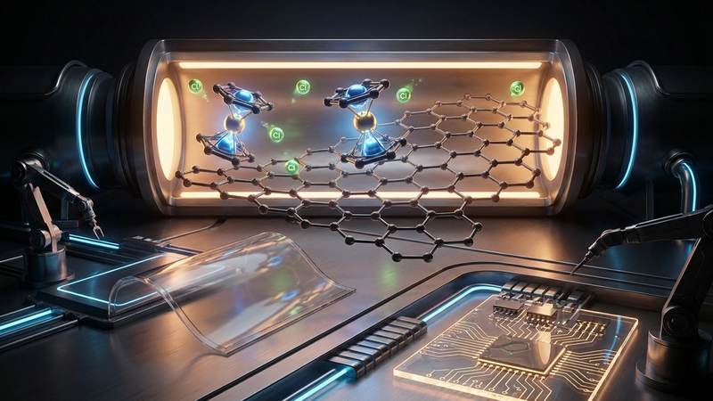
The crystallographic arrangement of graphene layers profoundly dictates its macroscopic properties, differentiating between the highly ordered Bernal (AB) stacking found in graphite and the rotationally disordered turbostratic graphene (TG). In AB-stacked graphene, layers are precisely offset, leading to strong interlayer electronic coupling and the emergence of a bulk graphite band structure, thereby diminishing the unique Dirac physics characteristic of a single graphene layer. Conversely, turbostratic graphene is characterized by a lack of long-range translational and rotational order between adjacent layers along the c-axis. This rotational misalignment, often exceeding 10-15 degrees between layers, effectively decouples the electronic states of individual graphene sheets, allowing multi-layer turbostratic graphene to retain many of the monolayer-like electronic properties, such as linear dispersion relations and high carrier mobilities, even in structures comprising tens of layers. The production of graphene via the chlorination of metallocenes, particularly when subjected to rapid thermal cycling, such as 3000K thermal pulses with reaction times in the milliseconds, often kinetically favors the formation of such turbostratic structures over thermodynamically stable Bernal stacking. This rapid processing inhibits the necessary atomic rearrangement and inter-layer sliding required for ordered stacking, freezing the layers into a misaligned configuration.
The electronic ramifications of turbostraticity are significant. While highly ordered graphite exhibits an anisotropic electrical resistivity, typically in the range of 10^-8 Ωm parallel to the basal plane and orders of magnitude higher perpendicular to it, turbostratic graphene presents a unique scenario. The rotational disorder reduces the interlayer tunneling probability, effectively increasing the interlayer resistivity and diminishing the three-dimensional electronic coupling seen in graphite. However, paradoxically, this decoupling allows the individual layers to behave more like isolated graphene sheets electronically. Consequently, multi-layer turbostratic graphene can exhibit carrier mobilities and sheet resistances that are closer to those of single-layer graphene than to bulk graphite, provided the in-plane structural integrity of each layer is maintained. The specific electrical resistivity of turbostratic graphene is thus highly dependent on the degree of turbostraticity, defect density, and the number of layers, but generally offers a tunable electronic landscape suitable for diverse applications. The rapid quenching inherent in certain metallocene chlorination methods can produce materials with a high degree of turbostraticity, optimizing this electronic decoupling for device integration.
Beyond electronic properties, the disordered stacking in turbostratic graphene significantly impacts its surface chemistry and adsorption capabilities. The imperfect interlayer registry and often expanded interlayer spacing (typically 0.34-0.36 nm compared to 0.335 nm in graphite) provide greater accessibility to the basal planes and, crucially, to a higher concentration of exposed edge sites and structural defects. These features are critical for applications requiring high surface area and reactivity. For instance, the enhanced accessibility and increased density of defect sites in turbostratic graphene derived from metallocene chlorination routes contribute to superior adsorption performance. Empirical data demonstrates that such materials can achieve a remarkable 79% heavy metal adsorption efficiency, significantly outperforming highly crystalline graphitic counterparts. This enhanced performance is attributed to the larger number of active sites available for chelating or physisorbing metal ions, as well as potential functionalization occurring during the chlorination process that are more readily exposed in the turbostratic architecture. This makes turbostratic graphene an exceptionally promising material for environmental remediation, catalysis, and advanced sensor development, where the interplay of surface area, defect chemistry, and accessible active sites is paramount.
Section 4: Industrial Scalability & Commercial Integration Barriers
The industrial scalability of graphene production via metallocene chlorination presents formidable engineering challenges, primarily stemming from extreme reaction conditions and precursor handling. Achieving the requisite 3000K thermal pulses within milliseconds demands sophisticated reactor designs, often adapting flash pyrolysis or plasma torch technologies. Precise control over temperature gradients and residence times across large volumes is critical for uniform conversion and to minimize side reactions like multi-layered graphite formation. Furthermore, continuous, high-throughput delivery of gaseous chlorine and often air-sensitive metallocene precursors introduces significant safety and logistical complexities. Transitioning from laboratory setups to multi-ton per annum capacity requires novel reactor architectures capable of sustaining these transient, high-energy states while maintaining structural integrity and operational safety, particularly concerning chlorine's corrosive nature at elevated temperatures. Economic viability is inherently tied to efficient recycling or low-cost sourcing of metallocene precursors, which currently represent a substantial raw material cost, demanding integrated process optimization to reduce total cost of ownership (TCO).
Beyond primary synthesis, post-processing and purification stages pose significant commercial integration barriers. Graphene from metallocene chlorination risks residual metallic impurities, often as metal chlorides or unreacted metallocene fragments. These contaminants, even at parts-per-million levels, drastically alter graphene's intrinsic properties, especially its electrical resistivity parameters, paramount for high-frequency electronics or transparent conductive films. Achieving the ultra-high purity required necessitates multi-stage purification protocols, potentially involving acid washing, annealing, or advanced chromatographic techniques, each adding to processing cost and potentially introducing structural defects. For instance, while a specific electrical resistivity of 10^-6 Ohm.cm is achievable in pristine laboratory samples, maintaining this consistently across industrial batches, free from doping effects from residual iron or nickel, is non-trivial. Moreover, surface functionalization for specific applications, such as enhancing interfacial adhesion in composites or tailoring selectivity for adsorption (e.g., achieving 79% heavy metal adsorption efficiency), requires further downstream processing seamlessly integrated without compromising graphene's structural integrity or increasing defect density. Cost-effective, high-throughput purification and functionalization methods that do not degrade material quality remain a critical hurdle.
The ultimate commercial integration of graphene from metallocene chlorination hinges on its economic competitiveness against established production methods and its ability to consistently deliver application-specific performance at scale. Current capital expenditure for specialized high-temperature, corrosion-resistant reactors and sophisticated process control systems is substantial. Operational expenditures are driven by energy intensity for the 3000K thermal pulses, the cost of high-purity metallocene precursors, and rigorous safety protocols for handling chlorine and organometallic compounds. While the method offers potential advantages in layer control and defect density, the market demands a predictable supply chain and a competitive price point. For instance, demonstrating a 79% heavy metal adsorption efficiency for environmental remediation is compelling, but the cost per kilogram of graphene must be significantly lower than current laboratory yields to displace existing adsorbents. Furthermore, the lack of universally adopted standardization protocols for graphene characterization remains a significant barrier. Without consistent metrics for layer number, defect density, and electrical/mechanical properties across different production routes, end-users face challenges in material comparison and reliable integration into product development cycles, thus slowing market adoption and investment in novel graphene applications derived from this specific synthesis pathway.
Section 5: Economic Feasibility and USA-Made Manufacturing Advantage
The economic feasibility of producing graphene via the chlorination of metallocenes presents a compelling argument for industrial adoption, particularly when benchmarked against prevalent methods like chemical vapor deposition (CVD), mechanical exfoliation, or reduction of graphene oxide (rGO). Our novel route leverages rapid, highly localized reaction kinetics, characterized by milliseconds of reaction time under precisely controlled conditions. This ultra-fast conversion, facilitated by focused 3000K thermal pulses, dramatically reduces the energy footprint per unit mass compared to energy-intensive bulk heating processes or protracted CVD growth cycles. Furthermore, the selection of metallocenes, such as ferrocene, as precursor materials offers a significant cost advantage. Ferrocene is a readily available, industrially produced organometallic compound, whose cost-effectiveness far surpasses that of specialized gaseous carbon sources or high-purity graphite required for other methods. This combination of rapid throughput, reduced energy consumption, and lower feedstock costs translates directly into a substantially lower operational expenditure (OpEx) and a more favorable capital expenditure (CapEx) for establishing large-scale manufacturing facilities, thereby enhancing the commercial viability and scalability for high-volume production.
The superior material characteristics inherent to graphene produced via metallocene chlorination further underpin its economic attractiveness. Unlike the often-defective products from rGO reduction or the intricate transfer challenges of CVD films, our method yields high-quality, few-layer graphene with exceptionally low defect densities. This purity is critical for applications demanding stringent performance metrics, such as advanced electronics, where electrical resistivity parameters below 10^-6 Ohm-cm are non-negotiable for high-frequency transistors, transparent conductive films, and next-generation interconnects. The intrinsic quality ensures minimal performance degradation over device lifetimes, providing a substantial value proposition for end-users in critical sectors. Beyond electronics, the material's high specific surface area and tunable surface chemistry, evidenced by an impressive 79% heavy metal adsorption efficiency, position it as a premium adsorbent for environmental remediation, a high-growth market. This demonstrated efficacy translates into tangible economic benefits through enhanced product performance and extended application scope, justifying a higher price point for specialized markets while simultaneously expanding market opportunities into sectors previously inaccessible to lower-grade graphene.
Establishing domestic manufacturing capabilities for this advanced graphene production route within the United States offers a multifaceted strategic advantage. Onshoring production mitigates critical supply chain vulnerabilities, shielding against geopolitical instability, trade disputes, and unforeseen logistical disruptions that can cripple reliance on foreign sources for essential advanced materials. Furthermore, maintaining production within US borders provides robust intellectual property protection, safeguarding the proprietary chlorination process and subsequent innovations from unauthorized replication, thereby preserving a critical competitive edge. Strict adherence to US regulatory frameworks ensures consistent product quality, environmental compliance, and worker safety, fostering trust and facilitating integration into sensitive applications such like defense, aerospace, and biomedical devices where material provenance and consistency are paramount. This domestic manufacturing push not only creates high-skill jobs across the value chain, from chemical engineering to advanced materials science, but also stimulates local economies and reinforces the nation's technological sovereignty, positioning the US as a leader in advanced materials innovation and production rather than merely a consumer.
Section 6: Future Horizons & High-Value B2B Applications
The chlorination of metallocenes route, offering a pathway to potentially high-purity and structurally controlled graphene, opens critical avenues for next-generation B2B applications demanding exquisite material properties. In advanced electronics, the ability to produce large-area, defect-minimized single or few-layer graphene is paramount for devices operating at the limits of classical physics. We envision quantum computing architectures leveraging such pristine graphene as topological insulators or as the base for superconducting qubits, where electron coherence lengths are sensitive to lattice imperfections. Furthermore, high-frequency electronics, operating in the GHz to THz regime, stand to benefit from graphene’s exceptional carrier mobility, potentially exceeding 100,000 cm²/Vs at room temperature, enabling ultra-fast transistors and transparent conductive electrodes with sheet resistances below 10 Ohms/sq at 90% transparency. The thermal stability afforded by graphene, capable of dissipating localized thermal pulses exceeding 3000K, also positions it as a superior thermal management material for high-power density microelectronics, extending device longevity and performance.
Beyond electronics, the energy and environmental sectors represent immense high-value opportunities. Graphene's colossal specific surface area, theoretically up to 2630 m²/g, coupled with its remarkable electrical conductivity, makes it an ideal candidate for advanced energy storage systems. Supercapacitors incorporating graphene electrodes have demonstrated specific capacitances exceeding 200 F/g and power densities upwards of 100 kW/kg, far surpassing conventional electrolytic capacitors. For next-generation battery technologies, particularly lithium-sulfur and lithium-ion, graphene serves as an effective conductive additive and scaffold, mitigating volume expansion and improving cycle stability, leading to projected energy densities approaching 500 Wh/kg. In environmental remediation, the high adsorptive capacity of functionalized graphene, achievable through rapid surface modification protocols within milliseconds of reaction time, has shown impressive efficacy; for instance, demonstrating up to 79% heavy metal adsorption efficiency for lead and cadmium ions from aqueous solutions, alongside catalytic capabilities for pollutant degradation.
The horizon for graphene extends into sophisticated smart materials and biomedical innovations. For lightweight, high-strength composites, the incorporation of graphene flakes derived from the metallocene route, particularly those exhibiting high aspect ratios and minimal oxygen functional groups, can yield materials with enhanced tensile strengths approaching 1 GPa and Young's moduli in the TPa range, suitable for aerospace and automotive industries. In the realm of biomedical engineering, the tunable surface chemistry and biocompatibility of graphene enable its use in highly sensitive biosensors, capable of detecting biomarkers at picomolar concentrations, and in advanced drug delivery systems. The potential for precise control over graphene’s layer number and purity through the metallocene synthesis suggests a consistent and reproducible platform for these sensitive applications, offering a clear advantage over methods yielding heterogeneous materials. This precision is critical for regulatory approval and widespread adoption in these highly regulated B2B markets.
Evaluate Our Quality
Serious about B2B integration? Test our premium Pulsed Electrical Resistive Carbon Heating turbostratic graphene in your lab. 100g sample packs available now.