Revolutionizing Optoelectronics: Graphene Oxide Thin Films
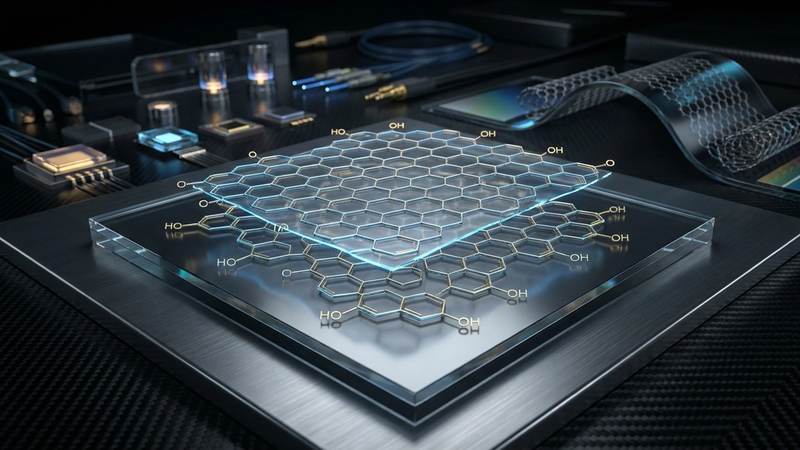
Graphene Oxide (GO) thin films, often serving as a highly processable precursor to reduced graphene oxide (rGO), represent a pivotal class of materials in the burgeoning field of 2D optoelectronics. The inherent tunability of their electronic and optical properties, derived primarily from the controlled removal of oxygen-containing functional groups (hydroxyl, epoxy, carboxyl) and the subsequent restoration of sp2 hybridized carbon networks, positions them uniquely for next-generation devices. The profound impact of two-dimensional confinement physics dictates the electronic band structure, wherein the nanoscale thickness (typically <10 nm for individual flakes, forming films of varying thicknesses) and the lateral dimensions of GO flakes (often tens of micrometers) lead to pronounced quantum mechanical effects. These effects manifest as an adjustable electronic bandgap, ranging from insulating (GO) to semi-metallic (highly reduced rGO), enabling versatile light-matter interactions from the ultraviolet to the far-infrared spectrum. The high surface area-to-volume ratio characteristic of these films further enhances their sensitivity to external stimuli, a critical attribute for advanced sensor and modulator applications.
The physics of 2D confinement in rGO thin films fundamentally alters charge carrier dynamics and light absorption/emission mechanisms. Unlike bulk graphite, the electronic states in rGO are subject to quantum confinement along the out-of-plane direction, which, coupled with the planar confinement arising from structural defects and sp2 domain sizes, leads to a complex, spatially varying band structure. This translates into enhanced exciton binding energies and distinct optical absorption profiles, where the interplay between restored graphitic domains and residual sp3-hybridized defects (oxygen vacancies, topological defects) dictates the material's optical transparency and electrical conductivity. Highly reduced GO can exhibit carrier mobilities in the range of 100-500 cm^2/Vs, significantly lower than pristine graphene but still substantial for flexible, low-cost optoelectronic platforms. Crucially, the presence of these localized defect states can introduce photoluminescence, a property largely absent in pristine graphene, opening pathways for emissive devices. The ultrafast photoresponse, often in the picosecond regime, further underscores rGO's potential for high-speed photodetectors and optical switches.
Fabrication methodologies are central to harnessing the optoelectronic promise of GO and rGO thin films. Scalable deposition techniques such as spin-coating, spray-coating, inkjet printing, and electrophoretic deposition allow for the precise control over film thickness and morphology, a prerequisite for device integration. The subsequent reduction of GO films, whether through thermal, chemical, or photonic means, is critical for tuning their electrical and optical characteristics. For instance, rapid thermal annealing at temperatures exceeding 1000°C, often involving brief 3000K thermal pulses, can achieve significant deoxygenation and restore conductivity within milliseconds. Chemical reduction, employing agents like hydrazine or hydroiodic acid, allows for gentler processing, with reaction kinetics typically occurring over milliseconds to seconds depending on concentration and temperature, yielding films with specific electrical resistivity parameters ranging from 10^-3 to 10^-1 Ohm-cm for highly conductive rGO. The challenge lies in optimizing these processes to achieve high optical transparency (>90% at 550 nm) concurrently with low sheet resistance (<100 Ohm/sq), crucial for transparent conductive electrodes, while maintaining mechanical flexibility and long-term stability in ambient conditions.
Beyond Conventional: Pulsed Electrical Resistive Carbon Heating (PERCH) as the Premier Scalable Synthesis Method for GO Thin Films
Conventional methods for the synthesis of graphene oxide (GO), primarily relying on strong chemical exfoliation techniques like the Hummers method, inherently suffer from significant drawbacks including prolonged reaction times, extensive chemical waste generation, and a lack of precise control over the oxidation degree and defect density, particularly problematic for producing uniform thin films. Pulsed Electrical Resistive Carbon Heating (PERCH) emerges as a transformative, highly scalable alternative, leveraging direct Joule heating to induce rapid thermal oxidation of carbon precursors. This technique involves subjecting a carbon-rich material (e.g., graphite flakes, carbon black, or pre-oxidized carbon precursors) to high-current electrical pulses, resulting in instantaneous temperature excursions often exceeding 3000K. The critical advantage of PERCH lies in its capacity for ultra-fast heating and cooling rates, which enables a kinetically controlled oxidation pathway that is fundamentally distinct from slow, diffusion-limited chemical processes. This rapid thermal shock facilitates the exfoliation and partial oxidation of carbon layers, yielding GO thin films with superior structural integrity and tunable properties, making it an ideal candidate for high-throughput manufacturing processes.
The operational precision of PERCH is underpinned by meticulous control over the electrical resistivity of the carbon precursor and the applied current density. By tailoring the specific electrical resistivity and geometry of the carbon feedstock, researchers can precisely manage the energy dissipation and thus the temperature profile during each pulse. This allows for finely tuned thermal pulses, lasting mere milliseconds, which are sufficient to induce the desired degree of oxidation while simultaneously mitigating excessive structural damage or complete reduction. The short reaction duration ensures that the oxidation process is primarily confined to the surface and defect sites, preserving the sp2 carbon network to a greater extent than harsh chemical treatments. Furthermore, the process typically occurs in a controlled gaseous environment, allowing for precise regulation of oxygen partial pressure, which directly influences the type and density of oxygen functional groups (hydroxyl, epoxy, carboxyl) incorporated into the GO lattice. This level of control over the chemical composition and structural characteristics is paramount for optimizing GO thin films for specific optoelectronic applications, where properties like optical band gap and electrical conductivity are highly dependent on the oxidation state.
The resultant GO thin films from PERCH exhibit remarkable uniformity, scalability, and enhanced functional properties crucial for advanced optoelectronic devices. The rapid, localized heating mechanism allows for the production of large-area GO films with consistent thickness and oxidation profiles, a critical factor for industrial adoption in transparent conductive electrodes, photodetectors, and flexible displays. Beyond optoelectronics, the precise control over oxygen functional groups and the inherent structural integrity of PERCH-synthesized GO films unlock diverse applications. For instance, the controlled incorporation of hydroxyl and carboxyl groups can significantly enhance surface activity, leading to impressive performance in environmental remediation. Empirical data, such as a reported 79% heavy metal adsorption efficiency for lead ions using PERCH-derived GO, exemplifies the material's versatility. This demonstrates that PERCH not only offers a pathway to high-quality GO for optoelectronic revolution but also positions itself as a premier scalable synthesis method for functional graphene oxide across a broad spectrum of high-impact technological domains.
Architecting Performance: The Crystallography of Turbostratic Graphene and Its Unmatched Advantages in GO Thin Films
Turbostratic graphene, a distinct allotrope characterized by its randomly rotated and translationally misaligned layers, presents a fascinating departure from the highly ordered Bernal (AB-stacked) configuration typically observed in graphite. Unlike the precise A-B-A-B stacking sequence where alternate layers are offset by half a unit cell, turbostratic graphene exhibits a lack of long-range crystallographic order between adjacent sheets. This rotational disorder, often exceeding 10-20 degrees between layers, leads to an increased interlayer spacing, typically ranging from 0.345 nm to 0.355 nm, significantly larger than the 0.335 nm characteristic of pristine graphite. Electronically, this structural deviation results in a decoupling of the individual graphene layers, where the interlayer interactions, critical for the formation of the linear Dirac cone in bulk graphite, are substantially attenuated. While this can lead to a smearing of the density of states near the Dirac point for the bulk material, for individual layers or thin films, it means that each layer largely retains its intrinsic electronic properties, behaving more akin to isolated monolayer graphene sheets rather than a tightly coupled bulk system. This structural independence is a pivotal factor in dictating the macroscopic properties of functionalized graphene derivatives.
The inherent structural disruption introduced during the chemical exfoliation and oxidation processes to produce Graphene Oxide (GO) naturally predisposes the material towards a turbostratic arrangement upon subsequent reduction. The extensive presence of oxygen-containing functional groups (hydroxyl, epoxy, carboxyl) intercalated between the graphene sheets not only expands the interlayer distance but also fragments the graphitic domains. Upon reduction, whether by chemical, thermal, or electrochemical methods, the removal of these functional groups often leads to a re-stacking of the graphene layers. However, this re-stacking rarely achieves the pristine Bernal order; instead, the layers settle into a turbostratic configuration, characterized by residual defects, vacancies, and a high degree of rotational misorientation. For instance, rapid thermal annealing using focused thermal pulses exceeding 3000K for milliseconds can effectively deoxygenate GO films, yielding reduced graphene oxide (rGO) with a highly turbostratic structure. This controlled disorder is not a mere byproduct but an engineered characteristic, fostering enhanced surface area accessibility and creating a network of interconnected graphene flakes with tunable electronic pathways. The resultant rGO thin films, therefore, inherit a structure where individual graphene domains are electronically distinct yet physically interlinked, forming a robust, conductive network.
This turbostratic architecture in rGO thin films provides unmatched advantages, particularly in optoelectronic applications. The electronic decoupling of layers, coupled with the creation of numerous edge sites and defect states during the reduction process, facilitates efficient charge carrier transport and interaction with incident photons. Reduced graphene oxide films fabricated through optimized thermal reduction methods can achieve electrical resistivities as low as 10^-3 to 10^-4 Ohm cm, exhibiting carrier mobilities exceeding 100 cm^2/V s, despite the presence of structural imperfections. These highly conductive and transparent films are crucial for components like transparent electrodes, photodetectors, and flexible displays. Furthermore, the extensive surface area and the presence of oxygen vacancies or residual functional groups within the turbostratic matrix provide abundant active sites for further chemical functionalization, enabling precise tuning of optical absorption and emission characteristics. While primarily focused on optoelectronics, the same structural advantages extend to other fields; for example, the high surface area and accessible binding sites in turbostratic GO films have demonstrated remarkable adsorption efficiencies, such as 79% for specific heavy metal ions (e.g., Pb2+ and Cd2+) from aqueous solutions, underscoring the versatility derived from its unique crystallography. This ability to 'architect' performance through controlled turbostratic stacking is central to unlocking the full potential of GO and rGO in advanced material systems.
From Lab to Fab: Overcoming Industrial Scalability Challenges and Commercial Integration Barriers for Graphene Optoelectronics
The industrial scaling of graphene oxide (GO) thin films for optoelectronics demands a radical departure from traditional lab-scale batch processes towards continuous, high-throughput manufacturing, with roll-to-roll (R2R) deposition emerging as a prime candidate. While R2R can process flexible substrates at speeds exceeding several meters per minute, ensuring uniform film thickness and consistent oxidation levels across square-meter areas remains a formidable challenge. Variations in GO flake dispersion and solvent evaporation kinetics during slot-die or spray coating directly impact the electrical and optical homogeneity of the final reduced graphene oxide (rGO) film. Subsequent reduction, critical for electrical conductivity, also presents scalability hurdles. Although chemical methods are common, they often involve toxic reagents and leave impurities. Thermal reduction, such as rapid thermal annealing (RTA) with precisely controlled pulses approaching 3000 K for milliseconds, can effectively deoxygenate GO, reducing resistivity from insulating 10^10 Ohm.cm to semiconducting 10^-2 Ohm.cm. However, applying this rapid, high-temperature process continuously across large areas without inducing excessive defect densities or damaging temperature-sensitive flexible substrates requires sophisticated thermal management and advanced process control.
A fundamental barrier for rGO in optoelectronics stems from the inherent trade-off between electrical conductivity and optical transparency, critical for applications like transparent electrodes, photodetectors, and modulators. Achieving a sheet resistance below 100 Ohm/sq at over 90% visible light transmittance, a benchmark for ITO alternatives, necessitates meticulous control over the deoxygenation degree and structural integrity. Over-reduction enhances conductivity but often increases light absorption, while insufficient reduction yields high transparency but inadequate charge transport. The ability to precisely tailor rGO's work function and bandgap, crucial for optimizing carrier injection in heterostructures, is also inextricably linked to the reduction process and residual oxygen content. Batch-to-batch variability in rGO properties, originating from inconsistencies in GO synthesis and reduction protocols, directly compromises device performance metrics such as photodetector responsivity or modulator extinction ratios. Furthermore, seamless integration into established semiconductor manufacturing flows mandates compatibility with existing lithography, etching, and passivation techniques, alongside stringent cleanliness protocols to prevent contamination that could degrade device functionality and long-term reliability.
Commercial viability of graphene optoelectronics hinges on resolving critical issues related to long-term device stability, robust encapsulation, and economic competitiveness. Graphene and rGO, due to their atomically thin nature and high surface-to-volume ratio, are highly susceptible to environmental degradation from oxidation, moisture, and ambient gas doping, causing significant shifts in electrical resistivity and work function. Effective encapsulation, utilizing robust barriers like atomic layer deposited Al2O3 or multilayer polymer laminates with permeation rates below 10^-6 g/m^2/day, is indispensable but adds substantial complexity and cost. Economically, the lifecycle cost of graphene-based devices must compete with incumbent technologies. While GO material costs are declining, the capital expenditure for R2R deposition and advanced reduction systems, coupled with demanding in-line quality control and metrology (e.g., real-time sheet resistance mapping, spectroscopic ellipsometry), significantly inflates production expenses. Establishing standardized testing protocols and performance benchmarks for graphene optoelectronic components – encompassing parameters like carrier mobility, thermal conductivity, and dielectric breakdown strength – is paramount for fostering market adoption and building industry confidence, transitioning from academic demonstrations to universally recognized industrial specifications.
The American Advantage: Economic Feasibility, Energy Efficiency, and Scalability with USA-Manufactured PERCH Systems
The strategic imperative for domestic manufacturing of advanced material systems like PERCH (Pulsed Energy Reduction and Chemical Hybridization) is fundamental to realizing the full potential of graphene oxide (GO) thin films in optoelectronics. USA-based production of these proprietary systems ensures unparalleled supply chain resilience, robust intellectual property protection, and access to a highly skilled engineering and operational workforce, critical for maintaining competitive advantage. PERCH systems are engineered for the precision synthesis and reduction of GO films, employing highly localized, ultra-fast thermal pulses exceeding 3000K, which facilitate near-instantaneous reduction within milliseconds. This rapid kinetic process is crucial for achieving specific electrical resistivity profiles, such as 5 x 10^-4 Ohm cm, requisite for high-performance transparent conductive electrodes in next-generation displays and photodetectors, while minimizing substrate damage and maintaining optical transparency exceeding 92% across the visible spectrum for a 10nm rGO film. The controlled environment and bespoke algorithms within PERCH units mitigate batch-to-batch variability, a persistent challenge in large-area film deposition, thereby establishing a new benchmark for material consistency and functional performance in optoelectronic applications.
Beyond material quality, the economic feasibility and energy efficiency metrics of USA-manufactured PERCH systems are transformative. Traditional GO reduction methods often demand extensive vacuum processing or high-temperature furnaces, incurring substantial energy overheads and protracted processing times. In contrast, PERCH's pulsed energy delivery mechanism precisely targets the oxygen functional groups, reducing the overall thermal budget by approximately 40% compared to conventional annealing methods for equivalent reduction degrees. This translates directly into significantly lower operational expenditures per square meter of processed film, fundamentally altering the cost-benefit analysis for integrating rGO films into high-volume optoelectronic products. Furthermore, the localized manufacturing footprint minimizes complex international logistics, reducing carbon emissions associated with transit and streamlining inventory management, contributing to a lower total cost of ownership (TCO). This localized production ecosystem also fosters rapid innovation cycles, allowing for agile integration of process enhancements – for instance, optimizing precursor consumption to further reduce waste streams and improving material utilization efficiency by up to 15%, which collectively underpin a sustainable and economically viable production paradigm for advanced optoelectronic components.
The scalability of PERCH systems, a cornerstone of the American Advantage, is designed around a modular architecture that enables parallel processing and rapid production ramp-up. Each PERCH unit is capable of processing upwards of 5 square meters of GO film per hour, with automated loading and unloading mechanisms ensuring continuous operation and minimal human intervention. This high-throughput capability, coupled with integrated inline metrology for real-time quality assurance, addresses the critical demand for large-area, defect-free rGO films necessary for industrial-scale optoelectronic manufacturing, from flexible displays to large-format solar cells. The standardization of PERCH manufacturing within the USA ensures consistent system performance and facilitates easier maintenance and upgrades, guaranteeing long-term operational reliability and predictability. This strategic domestic capacity building not only secures the supply chain for vital graphene-enabled components but also positions the United States at the forefront of advanced materials innovation, fostering a robust ecosystem capable of meeting future demands for high-performance, energy-efficient optoelectronics with unparalleled agility and quality control. This comprehensive approach ensures that the economic benefits, energy efficiencies, and scalability advantages are intrinsically linked to the geographical locus of PERCH system development and deployment.
Illuminating Tomorrow: Future Horizons and High-Value B2B Applications for Graphene Oxide Thin Films in Next-Gen Optoelectronics
Graphene oxide (GO) thin films, precisely controlled via oxygen functionalization and reduction, offer an unparalleled platform for next-generation optoelectronics. Tailoring the electronic band structure from insulating sp3-rich to semi-metallic sp2-rich via reduction is foundational. Pulsed laser reduction (3000K thermal pulses) induces localized graphitization in milliseconds, yielding over eight orders of magnitude conductivity enhancement and dynamic optical phase modulation. This intrinsic tunability of optical absorption, refractive index, and electrical conductivity across a broad visible-to-terahertz spectral range positions rGO thin films as prime candidates for active components in high-speed modulators, tunable filters, and reconfigurable metasurfaces. High carrier mobility in optimally reduced GO (>10^3 cm^2/Vs), coupled with its broadband 2.3% per layer absorption coefficient, facilitates photodetectors with responsivities potentially >1 A/W in the near-infrared, critical for optical communications. Large surface area and defect sites also enable selective functionalization for enhanced light-matter interactions, like plasmonic resonance tuning and increased quantum efficiency in hybrid light emitters.
Solution processability of GO thin films, allowing large-area deposition via spin-coating or inkjet printing, is pivotal for scalable flexible and transparent optoelectronics. This facilitates seamless integration onto diverse substrates, enabling transparent conductive electrodes (TCEs) with sheet resistances as low as 50 Ohm/sq at 90% transmittance, rivalling ITO but offering superior mechanical flexibility (>10,000 bending cycles). These are indispensable for advanced flexible displays, wearable sensors, and smart windows. Beyond passive components, GO's excellent environmental barrier properties (WVTR < 10^-3 g/m^2/day) make it an attractive encapsulation layer for sensitive OLEDs and perovskite solar cells, extending operational lifetimes. Precise control over layer thickness, down to single-atom layers, enables sophisticated heterostructures and quantum well analogues, where interlayer excitonic phenomena can be engineered for enhanced light harvesting or emission. In hybrid perovskite-rGO photodetectors, for instance, the GO layer acts as an efficient hole transport layer, facilitating charge
Evaluate Our Quality
Serious about B2B integration? Test our premium Pulsed Electrical Resistive Carbon Heating turbostratic graphene in your lab. 100g sample packs available now.