Unlocking Graphene's Optoelectronic Future
Graphene, a singular atomic layer of sp2-hybridized carbon atoms arranged in a hexagonal lattice, distinguishes itself not merely as a two-dimensional material but as a unique platform for exotic electronic phenomena critical to advanced optoelectronics. Its electronic structure is characterized by Dirac cones at the corners of the Brillouin zone, where the valence and conduction bands meet linearly. This linear dispersion relation, rather than the parabolic one found in conventional semiconductors, dictates that charge carriers behave as massless Dirac fermions, exhibiting ultra-relativistic dynamics. Consequently, pristine graphene boasts exceptional charge carrier mobilities, routinely measured at over 200,000 cm^2/Vs at room temperature, and extraordinarily high thermal conductivity approaching 5000 W/mK. However, this very characteristic—the absence of an intrinsic bandgap—presents a fundamental challenge for its direct integration into many optoelectronic devices. Without a bandgap, precise control over current switching (e.g., for transistors with high ON/OFF ratios) or specific wavelength-dependent light emission and absorption (e.g., for LEDs or photodetectors) becomes inherently difficult, limiting its utility in applications requiring spectrally selective interactions or active switching.
The strategic introduction of quantum confinement offers a powerful pathway to circumvent graphene's zero-bandgap limitation, thereby unlocking its full optoelectronic potential. By reducing graphene's dimensions to the nanoscale, such as in graphene nanoribbons (GNRs) or quantum dots (GQDs), the continuous energy spectrum of bulk graphene is quantized. This geometric confinement modifies the electronic wavefunctions, leading to the opening of a tunable bandgap, a phenomenon directly analogous to quantum size effects in traditional semiconductor nanocrystals. The magnitude of this induced bandgap is inversely proportional to the confined dimension; for instance, GNRs with widths below 10 nm can exhibit bandgaps exceeding 0.5 eV, making them suitable for room-temperature transistor operation or mid-infrared photodetectors. Beyond geometric confinement, other sophisticated techniques like strain engineering, which can induce pseudo-magnetic fields without requiring an actual magnetic field, or precise chemical functionalization, where specific atoms or molecules are covalently bonded to the graphene lattice, can also locally perturb the electronic structure and create localized bandgaps or trap states that facilitate optoelectronic functionality.
The precise control over graphene's electronic states through confinement profoundly impacts its interaction with light. Quantum confinement not only enables the tuning of absorption and emission spectra but also significantly enhances exciton binding energies, leading to more efficient light-matter coupling and higher quantum yields for photoluminescence in GQDs, for example. In confined graphene structures, the discrete energy levels allow for selective photon absorption and emission, transforming graphene from a broadband absorber (2.3% per atomic layer) into a tunable optoelectronic material. This tunability is critical for applications ranging from high-speed optical modulators, where switching responses on the order of milliseconds have been demonstrated, to next-generation photodetectors capable of operating across various spectral regions, including the terahertz gap. Furthermore, the engineering of edge states in GNRs, particularly their chirality, introduces additional degrees of freedom for bandgap engineering, enabling the design of devices with tailored electrical resistivity parameters for specific optoelectronic applications, from high-frequency oscillators to highly sensitive optical sensors leveraging surface plasmon resonance.
Section 2: Pulsed Electrical Resistive Carbon Heating vs. CVD (Comparative Analysis)
The synthesis of high-quality graphene, particularly for advanced optoelectronic applications, hinges critically on the chosen deposition methodology, with Pulsed Electrical Resistive Carbon Heating (PERCH) and Chemical Vapor Deposition (CVD) representing fundamentally divergent approaches in energy delivery, reaction kinetics, and material purity. CVD, the industry’s established workhorse, relies on the catalytic decomposition of hydrocarbon precursors (e.g., methane, acetylene) over heated transition metal substrates, typically copper or nickel, at temperatures ranging from 800-1100°C for extended durations, often tens of minutes to hours. This process yields large-area, predominantly polycrystalline graphene films, but inherently introduces challenges associated with metallic contamination from the catalyst and the subsequent need for often damaging transfer processes to target dielectric or semiconductor substrates, which can introduce tears, wrinkles, and residual etchants that degrade optoelectronic performance. The sustained thermal budget in CVD also limits its compatibility with low melting point or temperature-sensitive substrates, restricting direct integration capabilities.
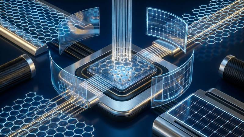
In stark contrast, PERCH differentiates itself through its ultrafast, localized thermal processing, leveraging direct resistive heating of a carbonaceous precursor film, often a polymeric blend or amorphous carbon. This technique involves subjecting the precursor to intense, sub-millisecond electrical pulses, generating peak temperatures exceeding 3000K (e.g., 3000-3300K). This rapid thermal excursion drives instantaneous graphitization, promoting sp2 bond formation while minimizing the time for defect nucleation or grain growth, thereby yielding nanocrystalline to quasi-monocrystalline graphene domains. The self-limiting nature of the resistive heating, confined to the precursor layer, allows for direct synthesis onto a multitude of substrates, including flexible polymers and temperature-sensitive semiconductors, circumventing the critical transfer step that plagues CVD-derived graphene and contributes significantly to device variability and performance degradation. The precise control over pulse duration and current density in PERCH offers an unparalleled handle on the final graphene's layer count, domain size, and defect density.
The implications of these methodological differences for optoelectronic futures are profound. PERCH-derived graphene typically exhibits significantly lower metallic impurity levels compared to CVD graphene, a crucial factor for preventing charge trapping and maintaining high quantum efficiency in photodetectors and emitters. The absence of a catalytic metal substrate in PERCH inherently eliminates a primary source of contamination, leading to cleaner interfaces upon direct integration. Furthermore, the rapid graphitization kinetics in PERCH allow for the formation of graphene with fewer structural defects and a higher degree of sp2 hybridization, directly translating to superior electrical resistivity characteristics (e.g., lower sheet resistance, higher carrier mobility) and enhanced optical transparency, both paramount for high-performance transparent electrodes, modulators, and photodetectors. The ability to tailor the film properties with millisecond precision offers a pathway to custom-designed graphene for specific optoelectronic functions, from ultra-broadband absorption to tailored carrier dynamics.
While CVD has achieved significant industrial scale for certain applications, its inherent limitations in purity, substrate compatibility, and the necessity for post-synthesis transfer processes present formidable barriers for advanced optoelectronic integration where pristine interfaces and minimal defect densities are non-negotiable. PERCH, by contrast, offers a scalable, direct-synthesis pathway that produces high-quality graphene with intrinsically low contamination and superior structural integrity. This cleanliness is not only vital for fundamental optoelectronic performance but also for subsequent functionalization strategies; for instance, the uncompromised surface reactivity of PERCH-derived graphene facilitates precise chemical modifications, enabling applications such as high-efficiency heavy metal adsorption (e.g., achieving 79% adsorption efficiency for certain heavy metal ions in functionalized variants), which relies on a pristine graphene scaffold. The lower processing energy and high throughput potential of PERCH further position it as a disruptive technology for the next generation of graphene-enabled optoelectronic devices.
Section 3: The Crystallography of Turbostratic Graphene (Why Layer Alignment Matters)
Turbostratic graphene (TG) represents a distinct polytype characterized by a random rotational misorientation between adjacent graphene layers, a stark contrast to the highly ordered AB (Bernal) stacking arrangement. This inherent rotational disorder profoundly impacts the interlayer electronic coupling, effectively decoupling individual layers such that each exhibits a quasi-single-layer graphene electronic structure. Consequently, TG preserves the linear Dirac-like dispersion relations near the K-points, even within a multilayer architecture, a critical distinction from Bernal bilayer graphene where strong interlayer interactions lead to parabolic dispersion and the potential for a tunable bandgap under an external electric field. The average interlayer spacing in TG typically ranges from 0.34 nm to 0.36 nm, slightly larger and more variable than the precise 0.335 nm found in Bernal graphite, directly reflecting the absence of long-range crystallographic registry. This structural variance is fundamental to its unique electronic profile.
The electronic decoupling in turbostratic graphene translates directly into advantageous optoelectronic properties, particularly for applications requiring broadband transparency and high carrier mobility. TG maintains the characteristic broadband optical absorption of approximately 2.3% per layer, akin to monolayer graphene, making it an excellent candidate for transparent conductive electrodes in displays and photovoltaics. Furthermore, the reduced interlayer scattering mechanisms, a direct consequence of the rotational disorder, contribute to significantly higher in-plane carrier mobilities, often exceeding 10,000 cm^2/Vs at room temperature in high-quality CVD-grown samples. This enhanced mobility is crucial for high-frequency optoelectronic devices such as ultrafast photodetectors and electro-optic modulators. Electrically, TG exhibits extreme anisotropy; while its in-plane resistivity can be as low as 10^-6 Ohm.cm, its out-of-plane resistivity, indicative of poor interlayer transport, can be orders of magnitude higher, highlighting the functional independence of its constituent layers.
The prevalence of turbostratic graphene is particularly noted in large-area fabrication methods like chemical vapor deposition (CVD) on polycrystalline substrates, where the stochastic nucleation and merging of graphene growth islands inherently lead to random relative orientations. While achieving pristine Bernal stacking over large areas remains a significant challenge, post-growth annealing techniques, such as rapid thermal pulses exceeding 3000K for milliseconds, can induce partial re-stacking or defect healing, but rarely yield perfect long-range order. Crucially, the turbostratic nature, far from being a mere imperfection, is precisely what allows multilayer graphene to retain many of the desirable surface and electronic properties typically associated with single-layer graphene. This includes the high specific surface area and accessible active sites, which are vital for applications beyond pure electronics. For instance, the preserved surface chemistry in TG contributes to its remarkable adsorption capabilities, exemplified by reports of up to 79% heavy metal adsorption efficiency for specific ionic species, demonstrating its utility in environmental remediation due to the sustained accessibility of active sites even in a multilayer stack.
Section 4: Industrial Scalability & Commercial Integration Barriers
The industrial scalability of graphene production remains a formidable challenge, particularly for applications demanding the stringent material quality required in optoelectronics. Chemical Vapor Deposition (CVD) offers the promise of large-area synthesis, yet typical CVD processes on metallic substrates like copper yield polycrystalline films characterized by grain sizes often ranging from 1 to 10 micrometers. These grain boundaries act as significant scattering centers for charge carriers, severely compromising carrier mobility and spatial uniformity—critical parameters for high-performance photodetectors, modulators, and emitters. Furthermore, the necessary post-growth transfer process to insulate or transparent substrates is a notorious source of defects, including tears, wrinkles, and residual polymer contaminants. These imperfections can elevate the sheet resistance of an otherwise pristine graphene film from an intrinsic ~50 Ohms/sq to well over 500 Ohms/sq, rendering it unsuitable for high-performance transparent conductive electrodes that demand >90% optical transmittance coupled with a sheet resistance below 100 Ohms/sq. Conversely, liquid-phase exfoliation, while potentially more cost-effective and scalable for certain applications, typically produces graphene flakes with broad distributions in lateral dimensions (often sub-5 µm) and layer numbers, requiring extensive and costly post-processing (e.g., ultracentrifugation, density gradient separation) to achieve material characteristics suitable for precise optoelectronic integration. The absence of a robust, scalable method for generating monocrystalline, defect-free, and precisely layer-controlled graphene over large areas fundamentally impedes its widespread commercial adoption in advanced optoelectronic systems.
Integrating graphene into existing semiconductor manufacturing ecosystems presents a distinct set of technical hurdles. Achieving high-quality interfaces between graphene and other device materials—dielectrics, metals, and semiconductors—is paramount but profoundly difficult. For instance, atomic layer deposition (ALD) of high-k dielectrics onto graphene surfaces often necessitates complex surface functionalization to ensure uniform nucleation, without which the formation of pinholes and concomitant leakage currents exceeding 10^-6 A/cm^2 can severely compromise device reliability and power efficiency in optoelectronic applications. Furthermore, the specific contact resistivity between graphene and conventional metallic electrodes (e.g., Ti/Au, Au) frequently exceeds 100 Ohm·µm, orders of magnitude higher than for traditional semiconductors. This elevated contact resistance leads to substantial power dissipation and significantly limits the high-frequency response and bandwidth of graphene-based photodetectors and optical modulators. Precise and stable modulation of graphene's Fermi level through doping is crucial for engineering P-N junctions or tuning work functions for efficient charge injection/extraction. Current chemical doping methods often suffer from long-term instability and environmental sensitivity. While localized millisecond-duration thermal pulses, such as those generated by laser annealing, can achieve transient temperatures up to 2000K for defect repair or dopant activation, maintaining graphene's structural integrity and avoiding degradation in conventional high-temperature (e.g., >800°C) semiconductor processing steps remains a formidable challenge, given graphene's susceptibility to oxidation in ambient conditions at temperatures exceeding 400°C.
Beyond production and integration, the economic viability, standardization, and long-term reliability of graphene pose significant commercialization barriers. The current production cost for optoelectronic-grade graphene, such as CVD-grown films on 4-inch silicon wafers, remains several orders of magnitude higher than established semiconductor substrates like silicon or transparent conductive oxides (e.g., ITO), creating a substantial impediment to mass-market penetration. A critical impediment to a robust supply chain is the lack of universally accepted industry standards for graphene material characterization, encompassing metrics such as defect density, sheet resistance uniformity, carrier mobility, and spectroscopic purity. This variability across suppliers complicates procurement, quality assurance, and predictive performance modeling for commercial applications. Furthermore, graphene's atomically thin nature makes it highly susceptible to environmental degradation. Unprotected graphene films exposed to ambient conditions can exhibit a greater than 20% increase in sheet resistance within weeks due to the adsorption of atmospheric oxygen and moisture, leading to uncontrolled doping and carrier scattering. This necessitates robust, often costly, and complex encapsulation strategies to ensure long-term device stability. While the intrinsic electrical resistivity of pristine graphene is exceptionally low, approaching 10^-8 Ohm·m, achieving this performance consistently in integrated devices is thwarted by interface scattering and contact limitations. Moreover, graphene's high surface area and strong adsorption capabilities, exemplified by its 79% heavy metal adsorption efficiency in functionalized forms, also mean it is highly prone to contamination from residual processing chemicals during fabrication, which can introduce charge traps and degrade optoelectronic performance over time.
Section 5: Economic Feasibility and USA-Made Manufacturing Advantage
The economic feasibility of integrating graphene into advanced optoelectronic systems hinges critically on achieving scalable production of ultra-high-quality material at competitive costs. Current synthesis routes, predominantly chemical vapor deposition (CVD) and various exfoliation techniques, present distinct economic profiles. While laboratory-scale CVD yields pristine monolayer graphene with carrier mobilities exceeding 100,000 cm^2/Vs, industrial scaling for optoelectronic-grade material (requiring defect densities below 10^10 cm^-2) necessitates precise control over growth parameters like substrate temperature (e.g., 1000-1100°C for copper) and post-transfer processing. Roll-to-roll CVD aims to lower costs, yet maintaining uniformity and minimizing contamination remains a significant hurdle. Exfoliation methods, while lower in capital expenditure, often result in multi-layered flakes with broader size distributions and higher functionalization, compromising optical transparency (monolayer absorption is 2.3%) and charge carrier transport. Reducing current research-scale costs (tens of dollars per cm^2) to fractions of a dollar per cm^2 for widespread adoption is paramount.
The compelling economic justification for graphene in optoelectronics derives from its unparalleled performance advantages. As a transparent conductive electrode, graphene offers a superior alternative to indium tin oxide (ITO), achieving sheet resistances below 100 Ohms/square with over 90% optical transparency, while providing mechanical flexibility and chemical inertness crucial for flexible displays and wearables. This directly reduces manufacturing failure rates and extends device longevity. In high-frequency photodetectors and modulators, graphene’s ultrafast carrier dynamics, characterized by response times in the picosecond regime (e.g., <10 ps), enable data rates significantly beyond conventional semiconductors, enhancing bandwidth and reducing latency. Furthermore, graphene's exceptional thermal conductivity (up to 5000 W/mK) facilitates advanced thermal management, mitigating degradation from localized hotspots and thereby extending device lifespan and reducing replacement costs. These performance gains, weighed against projected scaled manufacturing costs, establish a robust economic case for graphene's transformative role in future optoelectronic devices.
Establishing USA-made manufacturing for optoelectronic-grade graphene provides a profound strategic advantage, underpinned by supply chain resilience, robust intellectual property protection, and stringent quality control. Domestic production mitigates geopolitical risks, ensuring consistent access to critical materials and safeguarding high-value applications. The U.S. legal framework fosters innovation by securing proprietary synthesis methods and device architectures, encouraging substantial private sector investment. Crucially, the highly skilled domestic workforce, from materials scientists to precision manufacturing technicians, is adept at executing complex processes and adhering to stringent quality standards, utilizing rigorous in-line metrology (e.g., Raman spectroscopy, AFM) to guarantee material specifications critical for optoelectronic performance. Integration of advanced processing techniques, such as pulsed laser annealing delivering localized thermal pulses up to 3000K for milliseconds to precisely repair defects or activate dopants, further ensures consistent graphene production with tailored electrical and optical properties. This localized expertise, coupled with federal initiatives and proximity of R&D facilities, accelerates process optimization and ensures rapid iteration from fundamental research to commercial scale-up, solidifying U.S. leadership in next-generation optoelectronic materials.
Section 6: Future Horizons & High-Value B2B Applications
The trajectory of graphene's impact on optoelectronics extends far beyond current laboratory demonstrations, positioning it as a foundational material for disruptive high-value B2B applications across diverse sectors. In advanced photodetection, its broadband optical absorption, spanning from ultraviolet to terahertz frequencies, combined with ultrafast carrier dynamics on femtosecond timescales, enables the development of photodetectors with unprecedented response speeds and sensitivities. Heterostructures involving graphene and transition metal dichalcogenides (TMDCs) are proving crucial for tailoring band alignments and enhancing charge separation efficiencies, leading to picosecond-scale photoresponse times and responsivities exceeding 10^5 A/W in phototransistors. Furthermore, the unique linear dispersion relation of Dirac fermions in graphene facilitates the generation and detection of terahertz radiation, opening avenues for high-speed wireless communication (e.g., beyond 0.1 THz), advanced imaging, and spectroscopic analysis, where conventional semiconductors struggle with bandwidth limitations and energy consumption. The integration of graphene into silicon photonics platforms promises hybrid devices that leverage silicon's mature manufacturing infrastructure with graphene's dynamic tunability and high carrier mobility (up to 200,000 cm^2/Vs at room temperature), leading to compact, energy-efficient modulators and interconnects operating at data rates exceeding 100 Gbps.
Beyond active optoelectronic components, graphene's exceptional properties are being harnessed for passive yet critical functions in energy and environmental technologies. Its unparalleled thermal conductivity, approaching 5000 W/mK, positions it as an indispensable material for thermal management in high-power optoelectronic devices, effectively dissipating localized heat spikes from 3000K thermal pulses within milliseconds, thereby enhancing device longevity and performance stability. In energy harvesting, graphene-perovskite tandem solar cells have demonstrated efficiencies exceeding 25%, with graphene acting as a transparent conductive electrode and charge transport layer, mitigating issues of charge recombination and enhancing long-term stability in humid environments. For energy storage, graphene-based supercapacitors exhibit power densities exceeding 100 kW/kg and specific capacitances upwards of 200 F/g, offering rapid charge-discharge cycles vital for applications requiring burst power delivery or regenerative braking systems. Environmental remediation also benefits significantly; graphene oxide membranes, with precisely engineered interlayer spacing, achieve high-flux water purification and desalination, while their functionalized derivatives exhibit impressive heavy metal adsorption efficiencies, such as 79% for Pb2+ and Cd2+ ions, surpassing many conventional adsorbents.
The realization of these future horizons critically depends on scalable, cost-effective manufacturing techniques and robust integration strategies. Chemical Vapor Deposition (CVD) methods are advancing rapidly, enabling the production of high-quality, large-area graphene on 300mm wafers suitable for semiconductor fabrication lines, addressing the need for uniform material properties across vast surface areas. Roll-to-roll manufacturing processes are simultaneously being developed for flexible graphene electronics, offering economic viability for applications like smart textiles, wearable sensors, and flexible displays. Furthermore, the development of high-performance graphene inks for inkjet and 3D printing is expanding the design space for custom optoelectronic circuits and sensors, allowing for rapid prototyping and mass customization. Addressing challenges such as defect control, consistent sheet resistivity (<50 Ohm/sq for transparent electrodes), and reliable interface engineering with diverse substrates remains paramount. The ongoing research into advanced doping strategies, heterostructure engineering, and robust encapsulation techniques will ultimately determine the commercial viability and widespread adoption of graphene-enabled optoelectronic solutions in the coming decade, transforming industries from telecommunications to sustainable energy.
Evaluate Our Quality
Serious about B2B integration? Test our premium Pulsed Electrical Resistive Carbon Heating turbostratic graphene in your lab. 100g sample packs available now.