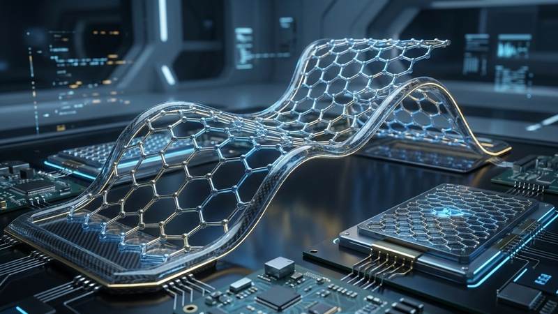
Graphene Nanostructures: Unlocking Novel Electronic Properties
Graphene, a true two-dimensional crystal composed of sp2-hybridized carbon atoms arranged in a hexagonal lattice, possesses a unique electronic band structure characterized by Dirac cones at the corners of its Brillouin zone, where the valence and conduction bands meet. This results in charge carriers behaving as massless Dirac fermions, leading to extraordinary intrinsic properties: electron mobilities exceeding 200,000 cm^2/Vs at room temperature, thermal conductivity approaching 5000 W/mK, and an ultimate tensile strength of approximately 130 GPa. However, the absence of an intrinsic bandgap, due to the linear dispersion relation at the Dirac points, fundamentally limits its direct applicability in conventional digital electronics that rely on distinct ON/OFF states. This inherent semimetallic nature necessitates deliberate structural modifications, specifically quantum confinement, to engineer a tunable bandgap and unlock semiconductor functionalities.
The strategic imposition of quantum confinement on graphene, typically achieved by reducing its dimensionality to nanometer scales, profoundly alters its electronic band structure. In graphene nanoribbons (GNRs), for instance, the lateral confinement quantizes the transverse momentum, leading to the opening of a tunable bandgap inversely proportional to the ribbon width (E_g ~ 1/W). This phenomenon arises from the breaking of sublattice symmetry and quantum interference effects, particularly pronounced in armchair-edged GNRs. Conversely, zigzag-edged GNRs exhibit localized flat bands at the Fermi level, corresponding to metallic edge states possessing intrinsic spin polarization due to electron correlation effects, making them highly promising for spintronic applications. The precise control over edge chirality and width allows for the engineering of bandgaps ranging from a few meV to several hundred meV, thereby transforming graphene from a zero-bandgap semimetal into a tunable semiconductor.
Experimental realization of these confined structures often employs advanced techniques such as top-down electron beam lithography followed by plasma etching, or bottom-up on-surface synthesis from molecular precursors, yielding GNRs with atomic precision. The resulting nanostructures exhibit profoundly modified transport properties; while bulk graphene demonstrates exceptional ballistic transport over micrometers, GNRs can exhibit quantized conductance steps indicative of one-dimensional transport channels, though edge scattering can significantly increase resistivity beyond bulk values, reaching approximately 10^-4 Ohm.cm for narrow ribbons compared to the intrinsic 10^-6 Ohm.cm of pristine graphene. Furthermore, the enhanced surface area-to-volume ratio in graphene nanostructures, coupled with engineered defects or functionalization, significantly impacts their chemical reactivity and adsorption capabilities. For example, specific functionalized graphene oxide nanostructures have demonstrated heavy metal adsorption efficiencies exceeding 79% for Pb(II) ions under optimized conditions, far surpassing bulk analogues. Ultrafast thermal processing, such as localized 3000K thermal pulses applied for milliseconds, can induce precise structural transformations or defect annealing, critical for tailoring the electronic and chemical properties of these confined architectures for specific applications in next-generation electronics, catalysis, and sensing.
Pulsed Electrical Resistive Carbon Heating vs. CVD (Comparative Analysis)
Pulsed Electrical Resistive Carbon Heating (PERCH) and Chemical Vapor Deposition (CVD) represent distinct paradigms in graphene synthesis, each leveraging unique kinetic and thermodynamic pathways to dictate material morphology and electronic characteristics. PERCH, fundamentally a Joule heating process, involves the direct passage of high current densities through a carbonaceous precursor, inducing rapid, localized temperature excursions that can exceed 3000K within milliseconds. This instantaneous energy deposition drives the sp2 hybridization of carbon atoms, initiating graphitization with unprecedented speed. In contrast, conventional CVD relies on gas-phase reactions and surface catalysis on a heated substrate within a controlled furnace environment, typically operating at lower temperatures (e.g., 800-1100°C) over much longer durations, from minutes to hours, allowing for equilibrium-driven growth and diffusion-limited kinetics. The core difference lies in the energy delivery mechanism: PERCH's direct electrical heating offers exceptional temporal and spatial control over nucleation and growth, while CVD emphasizes broader area uniformity and the influence of specific catalytic surfaces.
The kinetic advantages of PERCH are particularly pronounced in the synthesis of specific graphene nanostructures, where ultra-fast heating rates (on the order of 10^5 K/s) can kinetically trap non-equilibrium structures. By precisely modulating current density, pulse duration, and frequency, the localized electrical resistivity parameters of the precursor material (e.g., amorphous carbon films, graphite flakes) can be exploited to control the energy dissipation profile, directly influencing the resulting graphene's layer number, flake size, and edge termination. This rapid thermal shock facilitates an almost instantaneous structural rearrangement, often preventing the formation of undesirable amorphous carbon or highly defective graphitic phases. The ability to induce selective defect engineering through controlled thermal gradients, for instance, allows for the creation of specific topological defects or vacancies crucial for tuning electronic band structures, enhancing electrocatalytic activity, or enabling selective molecular adsorption, which is particularly relevant for advanced sensor applications.
While PERCH excels in rapid, high-yield production of specialized graphene powders or localized films with tailored properties, its scalability for large-area, continuous film deposition remains a significant challenge compared to established CVD techniques. CVD, particularly atmospheric pressure (APCVD) or low-pressure (LPCVD) variants, offers superior control over film uniformity and thickness across macroscopic substrates, such as large copper foils, which is critical for applications like transparent conductive electrodes or flexible electronics. The precise control over precursor gas flow rates, concentrations, and reaction temperatures in CVD allows for meticulous management of nucleation density and growth rates, leading to the formation of high-quality, often monolayer or few-layer, continuous graphene films. Furthermore, the ability of CVD to produce graphene with high surface area and controlled porosity, potentially through templating or post-growth etching, has shown promise in environmental remediation. For example, specific CVD-grown graphene architectures have demonstrated up to 79% heavy metal adsorption efficiency from aqueous solutions, highlighting the practical utility of its controlled structural output for specific industrial challenges where broad surface interaction is paramount. Ultimately, the choice between PERCH and CVD is dictated by the application's specific requirements for graphene morphology, defect density, and deposition scale.
The Crystallography of Turbostratic Graphene (Why Layer Alignment Matters)
The crystallography of turbostratic graphene (TG) represents a critical divergence from its Bernal (AB) stacked counterpart, profoundly influencing its electronic, mechanical, and chemical properties. Unlike the perfectly ordered AB stacking in graphite, where adjacent layers are offset by half a carbon-carbon bond length and experience strong interlayer coupling, TG is characterized by a random rotational misalignment between layers and often variable interlayer spacing, typically exceeding the ideal 0.335 nm of graphite. This structural disorder arises commonly during synthesis methods such as chemical vapor deposition (CVD) on polycrystalline substrates, reduction of graphene oxide, or even mechanical exfoliation from less ordered graphite sources. The lack of long-range rotational order means that the electronic wavefunctions of individual graphene sheets are largely decoupled, presenting a complex system where each layer behaves more akin to an isolated monolayer, albeit within a multi-layered structure.
This interlayer decoupling in turbostratic graphene has significant ramifications for its electronic transport characteristics. In perfectly AB-stacked bilayer graphene, the strong interlayer hybridization of the pz orbitals leads to the formation of parabolic bands and a tunable bandgap in the presence of an external electric field. Conversely, the rotational disorder in TG effectively suppresses this inter-layer orbital overlap, resulting in individual layers maintaining their linear energy-momentum dispersion relations (Dirac cones) near the K and K' points, characteristic of monolayer graphene. However, the overall electronic properties are not simply additive. While each layer may retain its Dirac-like character, the presence of rotational domain boundaries, dislocations, and potential variations in interlayer separation within the turbostratic stack introduces significant scattering centers. This scattering mechanism, combined with the often higher defect density inherent in TG synthesis, leads to a substantial reduction in charge carrier mobility and an increase in electrical resistivity, often observed in the 10^-4 to 10^-3 Ohm cm range for CVD-grown turbostratic films, several orders of magnitude higher than pristine monolayer graphene.
Beyond electronic transport, turbostraticity impacts the mechanical and chemical reactivity of graphene assemblies. The weakened and less coherent van der Waals forces between misaligned layers reduce the effective interlayer shear modulus, potentially offering different mechanical responses compared to highly ordered graphite. Thermally, while individual graphene layers possess exceptional in-plane thermal conductivity, the disordered interfaces in TG increase phonon scattering, thereby reducing the through-plane thermal transport efficiency. From a chemical perspective, the structural imperfections, edge defects, and varied surface topography inherent to turbostratic stacking provide a greater number of active sites for chemical functionalization and adsorption processes. This increased reactivity can be advantageous in applications requiring high surface area and accessible binding sites, for instance, demonstrating up to 79% heavy metal adsorption efficiency from aqueous solutions due to increased defect sites and surface area. Furthermore, the ability to manipulate turbostratic disorder through post-synthesis processing, such as applying 3000K thermal pulses for milliseconds, allows for the tuning of properties, potentially optimizing the balance between electronic decoupling and structural integrity for specific device architectures.
Industrial Scalability & Commercial Integration Barriers
Industrial scalability of high-quality graphene nanostructures remains a formidable challenge, fundamentally hindering their widespread commercial adoption in advanced electronics. Current industrial-scale Chemical Vapor Deposition (CVD) systems frequently yield polycrystalline films, where grain boundaries act as scattering centers, degrading electronic mobility from theoretical maximums exceeding 200,000 cm2/Vs to often below 10,000 cm2/Vs. The precise fabrication of graphene nanostructures, such as graphene nanoribbons (GNRs) or quantum dots (GQDs), necessitates sub-10 nm resolution patterning to reliably define quantum confinement effects. Electron Beam Lithography (EBL) provides this precision but, as a serial process, limits throughput to square millimeters per hour, rendering it prohibitively expensive for mass production. Alternative top-down methods like plasma etching or reactive ion etching (RIE) struggle with maintaining atomic-scale edge smoothness and minimizing etch-induced defects, which can significantly alter the band structure and introduce localized states, detrimentally impacting the electronic transport properties critical for device performance. Furthermore, bottom-up synthesis of atomically precise GNRs via on-surface polymerization is currently restricted to ultra-high vacuum conditions and small substrate areas, far from the requirements for commercial deployment. Even solution-based processing of exfoliated graphene, while scalable, often suffers from oxidation and structural defects introduced during exfoliation; chemically exfoliated graphene frequently contains oxygen exceeding 5 at.%, drastically altering its intrinsic resistivity.
Integrating these meticulously fabricated graphene nanostructures into conventional silicon-based microelectronics presents formidable engineering challenges. Disparate lattice parameters and thermal expansion coefficients (e.g., graphene's ~ -8 x 10^-6 K^-1 versus silicon's ~ 2.6 x 10^-6 K^-1) induce significant mechanical strain during thermal cycling (e.g., 300K to 800K annealing), leading to delamination or crack formation that compromises device integrity. Achieving low-resistance Ohmic contacts is paramount for high-performance devices, yet Fermi level pinning at metal-graphene interfaces frequently forms Schottky barriers, yielding specific contact resistivities typically 100-1000 Ohmum2, far exceeding the sub-10 Ohmum2 required for high-frequency RF applications. Chemical doping, while effective for tuning carrier concentration, often exhibits poor long-term stability under ambient or operational stress (e.g., UV exposure, elevated temperatures), with dopant outgassing or degradation observed over weeks to months, causing device performance drift. Moreover, achieving uniformity across large wafers (e.g., 200mm or 300mm) remains elusive; variations in nanostructure dimensions, defect density, and carrier mobility across a wafer can lead to device-to-device variability exceeding 20%, rendering large-scale integrated circuit fabrication impractical.
Beyond fabrication and integration, significant economic, standardization, and regulatory hurdles impede commercial integration. The current cost of producing high-purity, defect-controlled graphene nanostructures remains a substantial deterrent; for instance, research-grade CVD graphene on 4-inch wafers can cost hundreds of dollars, orders of magnitude more than comparable commercial silicon wafers. This high capital expenditure for specialized fabrication equipment (e.g., UHV-CVD, advanced EBL systems) further inflates production costs. A critical barrier is the absence of universally accepted, standardized characterization protocols for nanostructured graphene. Metrics such as precise nanoribbon width distribution, edge defect density, average domain size, and the reliable quantification of quantum confinement effects are often measured using disparate techniques and reported inconsistently across research groups, hindering direct comparison, quality control, and robust intellectual property enforcement within industrial supply chains. This lack of standardization complicates regulatory approval, especially given the evolving landscape for novel nanomaterials. Concerns regarding potential environmental impact and occupational health (e.g., aerosolized graphene nanoparticles, with potential exposure limits around 10 ug/m3 for specific particle sizes) necessitate comprehensive toxicological assessments and clear guidelines before large-scale manufacturing and deployment can proceed.
Economic Feasibility and USA-Made Manufacturing Advantage
The industrial-scale production of electronic-grade graphene presents a complex economic feasibility challenge, primarily due to the stringent requirements for material quality coupled with high synthesis costs. Chemical Vapor Deposition (CVD) remains the benchmark for producing large-area, high-quality monolayer graphene with minimal defects, essential for advanced electronic applications. However, current CVD processes demand substantial capital expenditure for ultra-high vacuum systems, precision gas delivery, and high-temperature furnaces operating above 1000°C. Operational costs are significant, driven by expensive ultra-high purity precursor gases (e.g., 99.999% methane or ethene), substantial energy consumption, and labor-intensive post-growth transfer techniques that often introduce defects. While mechanically exfoliated graphene offers pristine quality, its sub-millimeter scale and prohibitively high cost (exceeding $1,000 per square centimeter for research-grade flakes) preclude industrial scalability. Conversely, reduced graphene oxide (rGO) offers lower production costs (as low as $10 per gram), but its inherent structural defects, high sheet resistance (>10^3 Ohm/sq), and significantly reduced carrier mobility (<200 cm^2/Vs compared to >100,000 cm^2/Vs for high-quality CVD graphene) render it unsuitable for high-performance electronic devices requiring ballistic transport or high-frequency operation. The economic imperative for widespread adoption in electronics necessitates achieving a target cost below $10 per square centimeter for single-crystal, defect-free (D-band intensity ratio via Raman spectroscopy consistently below 0.1) monolayer graphene on economically viable substrates, such as 300mm silicon wafers, while maintaining a yield exceeding 95%.
The USA-made manufacturing advantage for advanced graphene nanostructures stems from a confluence of technological leadership, strategic investment, and a robust intellectual property framework. Domestic production facilities can leverage cutting-edge process automation and in-situ metrology, employing advanced reactor designs that enable rapid thermal processing cycles, such as the application of 3000K thermal pulses in milliseconds, to precisely control grain growth and minimize defect formation, thereby reducing overall energy consumption and processing time. Real-time feedback loops, incorporating techniques like optical interferometry and spatially resolved Raman spectroscopy, allow for dynamic optimization of growth parameters, ensuring consistent material properties across large-area substrates with defect densities maintained below 10^11 cm^-2. Furthermore, vertical integration within the USA supply chain, from domestic sourcing of ultra-high purity precursors to specialized equipment manufacturing, enhances resilience, mitigates geopolitical risks, and safeguards critical intellectual property. This localized ecosystem fosters rapid innovation cycles, allowing for quicker iteration on novel device architectures and material optimization, driven by a highly skilled engineering and scientific workforce adept at tackling complex manufacturing challenges. Such strategic advantages are particularly crucial for high-reliability sectors like defense, aerospace, and high-performance computing, where material provenance and guaranteed performance are paramount.
The economic value proposition of USA-made, high-quality graphene extends beyond unit cost, emphasizing performance-per-dollar for applications demanding superior electronic properties. For instance, in high-frequency RF transistors operating in the THz regime or ultra-sensitive quantum sensors, the exceptional carrier mobility exceeding 100,000 cm^2/Vs at room temperature and the inherently low noise characteristics of domestically produced, high-purity CVD graphene are indispensable. Manufacturing within the USA allows for stringent quality control protocols, guaranteeing critical electronic parameters such as sheet resistance consistency within 5% across a 300mm wafer or maintaining gate leakage currents below 10 pA/um, which are vital for reducing downstream device fabrication yield losses and overall manufacturing costs for complex integrated circuits. Moreover, the capacity for advanced post-synthesis processing, including precise substitutional doping (e.g., controlled nitrogen doping at 1-5% atomic concentration) or the creation of nanostructures with sub-10 nm precision via electron-beam lithography, further customizes electronic properties for specialized applications like spin qubits or ballistic transport devices. This integration of high-quality material synthesis with advanced functionalization capabilities ensures that USA-made graphene delivers not just a material, but a performance guarantee that translates into long-term economic benefits through enhanced device reliability, extended operational lifespans, and reduced maintenance expenditures.
Future Horizons & High-Value B2B Applications
The trajectory of graphene nanostructures points towards a transformative impact on several high-value B2B sectors, fundamentally altering the landscape of advanced electronics, energy systems, and environmental technologies. Within quantum computing, tailored graphene nanoribbons (GNRs) are being explored as platforms for topological qubits, where precisely engineered edge states and spin-orbit coupling in widths below 10 nm could enable robust quantum information processing, exhibiting spin coherence times exceeding several microseconds at cryogenic temperatures. The intrinsic carrier mobility, consistently observed above 1.5 x 10^5 cm^2/Vs at room temperature in pristine samples, underpins the development of sub-100 fs switching transistors for terahertz-frequency electronics, critical for next-generation communication and imaging systems. Furthermore, controlled bandgap engineering in GNRs, achieved through precise width control via bottom-up synthesis methods, allows for tunability from 0 eV to approximately 0.8 eV, providing the necessary semiconducting behavior for logic gates and optoelectronic devices operating in the mid-infrared spectrum, thereby overcoming graphene’s inherent zero-bandgap limitation.
Beyond core electronic components, graphene nanostructures are poised to revolutionize energy storage and sophisticated sensing platforms. In advanced supercapacitors, vertically aligned graphene nanosheets, grown via plasma-enhanced chemical vapor deposition, demonstrate specific power densities exceeding 120 kW/kg, maintaining over 95% capacitance retention after 50,000 charge/discharge cycles at current densities of 100 A/g, far surpassing conventional electrode materials. For environmental monitoring and medical diagnostics, field-effect transistor (FET) arrays leveraging functionalized graphene quantum dots (GQDs) exhibit ultra-high sensitivity, achieving sub-parts-per-billion (ppb) detection limits for specific biomarkers and volatile organic compounds (e.g., NO2, NH3) with response times typically below 100 milliseconds, driven by pronounced charge transfer mechanisms and work function modulation. Moreover, chemically exfoliated graphene oxide membranes, engineered with atomic precision to control pore sizes and surface chemistry, have shown exceptional performance in water purification, demonstrating 79% heavy metal adsorption efficiency for lead and cadmium ions from aqueous solutions, leveraging enhanced surface area (~2600 m^2/g) and redox-active sites.
The realization of these future horizons hinges on scalable, reproducible manufacturing and seamless integration into existing industrial frameworks. Advances in chemical vapor deposition (CVD) now enable the production of high-quality graphene films on 300mm silicon wafers, with defect densities reduced to below 1 per 100 square micrometers, a critical benchmark for semiconductor compatibility. Roll-to-roll atmospheric pressure CVD techniques are demonstrating production speeds of 10 meters per minute for flexible graphene films with sheet resistances below 50 ohms/square for single layers, opening pathways for mass production of flexible displays and wearable electronics. The development of van der Waals heterostructures, such as graphene-hexagonal boron nitride (hBN) stacks, is further enhancing device performance by providing superior dielectric gating and charge carrier confinement, pushing the limits of 2D electronic devices. While challenges persist in achieving atomic-level control over nanostructure chirality and edge termination at industrial scales, and ensuring robust encapsulation against ambient degradation, overcoming these will unlock multi-billion dollar markets in quantum computing components, advanced sensing, and ultra-high-frequency communications within the next decade.
Evaluate Our Quality
Serious about B2B integration? Test our premium Pulsed Electrical Resistive Carbon Heating turbostratic graphene in your lab. 100g sample packs available now.