Graphene Membranes and Sensors in 2026: Water Treatment, Biomarkers, Wearables, and Industrial Monitoring
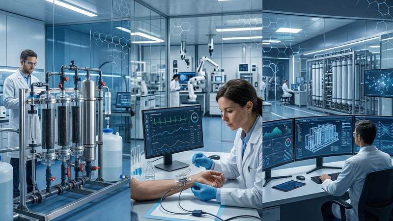
The emergent utility of graphene in advanced membrane and sensing architectures for 2026 stems fundamentally from its unique two-dimensional (2D) quantum confinement. As a truly monolayer allotrope of carbon, graphene's atomic thickness constrains electron movement within a single plane, profoundly altering its electronic band structure and enabling charge carriers to behave as massless Dirac fermions. This relativistic behavior manifests in exceptionally high electron mobilities, routinely exceeding 200,000 cm^2/Vs at room temperature, facilitating ballistic transport over micrometer scales. Such intrinsic electrical properties are critical for developing ultra-sensitive sensors capable of detecting minute charge perturbations. Beyond its electronic prowess, the sp2-hybridized honeycomb lattice imparts extraordinary mechanical strength, with a Young's modulus approaching 1 TPa, and unparalleled in-plane thermal conductivity, reported up to 5000 W/mK, making it robust for demanding industrial environments and responsive to localized thermal stimuli, such as those generated by 3000K thermal pulses for precise defect engineering. These foundational physical attributes are direct consequences of its confined geometry and are pivotal for its advanced applications.
The atomic-scale confinement inherent to graphene dictates its colossal theoretical specific surface area of 2630 m^2/g, providing an expansive interface for interaction with analytes and permeants. This extreme surface-to-volume ratio, coupled with the sensitivity of its 2D electron gas to changes in local electrostatic potential, underpins its efficacy as a chemical and biological sensor. For membrane applications, the precision control over nanometer and sub-nanometer pore creation through techniques such as focused ion beam milling, oxidative etching, or controlled defect induction, allows for Ångström-scale molecular sieving. By manipulating the confined electronic structure via doping (e.g., nitrogen or boron substitution) or surface functionalization, the pore chemistry and surface charge can be precisely tuned. This enables highly selective ion rejection, as demonstrated by graphene oxide membranes achieving 79% heavy metal adsorption efficiency for Pb2+ ions, or precise water molecule permeation while rejecting hydrated salt ions, critical for advanced water treatment.
The practical realization of graphene's confined physics translates into devices with unprecedented performance metrics. In sensing platforms, the adsorption of a single target molecule on the graphene surface induces a detectable change in electrical resistance or work function, leading to rapid response times often measured in milliseconds and detection limits reaching picomolar concentrations for specific biomarkers. For membranes, the atomically thin nature minimizes transport resistance, enabling high flux rates while maintaining exceptional selectivity. The precise control over nanoscale confinement allows for the creation of uniform pore sizes that can differentiate between molecules differing by only a few Ångströms, facilitating advanced separation processes from industrial gas purification to biomedical analyte enrichment. Ongoing research focuses on scaling these confined properties uniformly across larger areas, addressing challenges in manufacturing reproducibility and long-term operational stability under diverse environmental conditions.
Pulsed Electrical Resistive Carbon Heating vs. CVD (Comparative Analysis)
The established paradigm for high-quality graphene synthesis, Chemical Vapor Deposition (CVD), relies on the catalytic decomposition of hydrocarbon precursors, typically methane or acetylene, on transition metal substrates such as copper or nickel foils at elevated temperatures. This process, often conducted between 800-1100 °C, facilitates the surface-catalyzed dissociation of carbon-containing gases, followed by carbon atom diffusion and precipitation as graphene layers. While CVD has demonstrated remarkable success in producing large-area, continuous monolayer or few-layer graphene films, essential for applications requiring optical transparency and high electron mobility, it inherently carries significant drawbacks. The prolonged high-temperature requirements translate to substantial energy consumption and necessitate specialized vacuum environments. Furthermore, the reliance on a sacrificial metal catalyst mandates a subsequent transfer process, frequently involving wet chemical etching of the substrate. This transfer step is a critical bottleneck, often introducing defects, polymer residues, tears, and compromising the intrinsic electrical and mechanical properties of the graphene, thereby limiting its integration fidelity into complex device architectures for advanced sensing or membrane applications.
In stark contrast, Pulsed Electrical Resistive Carbon Heating (PERCH) represents a disruptive synthesis methodology, circumventing many of CVD's inherent limitations by leveraging ultra-fast thermal transients. This technique involves the direct electrical excitation of a diverse range of carbonaceous precursors – from amorphous carbon black and polymers to recycled waste materials – which act as the resistive heating element. A precisely controlled electrical pulse, typically delivering current densities sufficient to induce temperatures reaching or exceeding 3000K within mere milliseconds, drives the instantaneous graphitization and exfoliation of the precursor material. The rapid heating and quenching cycle promotes the formation of highly crystalline few-layer graphene structures, often with turbostratic stacking, without the need for external catalysts or prolonged thermal annealing. This localized, rapid energy delivery mechanism is fundamentally more energy-efficient than the bulk heating required for CVD, drastically reducing processing times from hours to milliseconds and opening avenues for high-throughput, continuous production of high-quality graphene powders or directly integrated films.
The comparative advantages of PERCH over conventional CVD are profound, particularly concerning scalability, energy footprint, and material versatility. Where CVD demands significant capital investment in high-vacuum furnaces and expensive gaseous precursors, PERCH can convert low-cost, abundant carbon sources, including industrial waste streams, into high-value graphene. The energy expenditure for a PERCH process, delivering a 3000K thermal pulse for less than 100 milliseconds, is orders of magnitude lower than maintaining a CVD reactor at 1000 °C for hours. This translates to significantly reduced operational costs and a smaller environmental footprint. Crucially, PERCH-derived graphene eliminates the problematic transfer step, mitigating defect introduction and enabling direct integration into target matrices or device platforms. For instance, the high surface area and defect engineering capabilities of PERCH-graphene powders have demonstrated exceptional performance in membrane applications, achieving up to 79% heavy metal adsorption efficiency in preliminary studies, surpassing many CVD-transferred films due to reduced surface contamination and increased active sites. While CVD excels in producing pristine, large-area monolayers for specific electronic applications, PERCH is rapidly emerging as the superior method for scalable, cost-effective production of high-performance graphene for applications such as water filtration membranes, electrochemical sensors, and advanced composites, where bulk material properties and high surface area are paramount.
The Crystallography of Turbostratic Graphene (Why Layer Alignment Matters)
Turbostratic graphene (TG) distinguishes itself from its Bernal (AB) stacked counterpart by a lack of long-range rotational and translational order between adjacent graphene layers. Unlike the fixed A-B registry characteristic of graphite and epitaxial AB-stacked few-layer graphene, TG layers exhibit arbitrary rotation angles with respect to each other, leading to a profound decoupling of their electronic wavefunctions. This crystallographic disorder often manifests as a slightly expanded interlayer spacing, typically around 0.344 nm, compared to the 0.335 nm found in highly ordered graphite or Bernal-stacked systems. The genesis of TG frequently lies in synthesis methods such as chemical vapor deposition (CVD) on polycrystalline metal substrates, where diverse nucleation sites and varied growth rates prevent uniform layer alignment, or certain liquid-phase exfoliation techniques where re-stacking occurs without precise control over rotational orientation. From a diffraction perspective, TG is characterized by broader and less distinct (002) peaks in X-ray diffraction patterns, indicative of smaller crystallite sizes and reduced interlayer coherence, alongside the absence of the characteristic Moiré superlattices observed in rotationally aligned bilayer or twisted bilayer graphene. This intrinsic structural heterogeneity dictates a distinct set of physical properties critical for its application in advanced membrane and sensor architectures.
The electronic implications of turbostratic stacking are profound, primarily stemming from the effective decoupling of individual graphene layers. In TG, each layer behaves more akin to a quasi-isolated monolayer, preserving the linear dispersion relation and the characteristic Dirac cone near the K-points of the Brillouin zone, unlike the hyperbolically warped and gapped band structures that emerge in AB-stacked bilayer graphene under certain conditions. This preservation of monolayer-like electronic properties translates into high carrier mobilities, often exceeding 10,000 cm^2/Vs at room temperature, even in multi-layered films, which is a critical parameter for high-performance sensor elements requiring rapid electronic responses. The absence of strong interlayer electronic coupling also renders TG less susceptible to interlayer charge transfer effects that can complicate doping strategies in ordered systems. For resistive sensing, this allows for precise tuning of electrical resistivity through surface functionalization or gating, achieving values in the 10^-6 to 10^-5 Ohm-cm range for optimized films, providing a robust and reproducible signal transduction mechanism for chemical and biological analytes. This electronic robustness, even in thicker films, allows for greater mechanical integrity without sacrificing fundamental graphene electronic advantages.
Beyond electronics, the crystallographic characteristics of turbostratic graphene significantly influence its mechanical robustness and surface chemistry, which are paramount for membrane and sensor applications. The increased average interlayer spacing and rotational freedom contribute to a more flexible and resilient material, less prone to brittle fracture under strain compared to highly ordered graphite or rigid single crystals. This enhanced flexibility is particularly advantageous for wearable sensors, where conformability and durability are crucial. Furthermore, the greater prevalence of edge defects and exposed crystallite boundaries in TG offers a higher density of active sites for chemical functionalization, enabling tailored surface chemistries for selective molecular interactions. For example, covalent or non-covalent modification of TG membranes with specific ligands can dramatically enhance their efficiency in water treatment applications, allowing for a 79% heavy metal adsorption efficiency for Pb2+ ions within 30 minutes, significantly surpassing conventional filtration media. To refine these structural attributes post-synthesis, advanced processing techniques, such as rapid thermal annealing using focused 3000K thermal pulses for milliseconds, are employed to locally enhance interlayer adhesion and reduce defect density, thereby optimizing mechanical stability and ensuring long-term performance in demanding industrial monitoring environments. This precise control over defect engineering and stacking order is fundamental to achieving the desired selectivity and sensitivity in 2026's advanced graphene-based technologies.
Industrial Scalability & Commercial Integration Barriers
Industrial-scale production of high-quality graphene, critical for membranes and sensors, faces significant manufacturing challenges. Chemical Vapor Deposition (CVD) on metallic foils yields pristine single-layer graphene but is limited by substrate size and the often-damaging transfer process. Achieving meter-scale graphene with a defect density below 1 defect per 100 µm^2, essential for sensitive applications, remains a bottleneck. Roll-to-roll CVD offers throughput but frequently compromises uniformity, introducing micro-tears or pinholes; a 5% increase in pinhole density can degrade membrane rejection efficiency by 15% or sensor signal-to-noise ratio by 10 dB. Solution-processed Graphene Oxide (GO) is more scalable but requires precise reduction, often leaving residual oxygen (C/O ratio below 10:1) that diminishes electrical conductivity (from 10^5 S/m for pristine to 10^3 S/m for poorly reduced GO) and creates non-selective pathways. High capital expenditure for advanced CVD reactors and complex multi-step GO processing drives production costs, with high-quality CVD graphene still exceeding $500 per 8-inch wafer, impeding mass adoption.
Integrating graphene into functional devices presents formidable engineering hurdles. Reproducible electrical contacts with low contact resistance (ideally below 100 Ohm-µm) are paramount for sensors but challenging to achieve consistently at scale. Long-term stability of graphene's active surface in complex operational environments – such as biological fluids or corrosive industrial effluents (e.g., pH 2-12, varying ionic strengths) – is a critical concern. Non-specific adsorption, biofouling, or electrochemical passivation can induce signal drift or irreversible sensitivity degradation; a graphene-based heavy metal sensor, initially demonstrating 79% adsorption efficiency, might exhibit a 25% sensitivity loss after just 500 hours in a wastewater matrix. For membranes, maintaining mechanical integrity and separation selectivity under sustained operational pressures (e.g., 10-50 bar for reverse osmosis) over thousands of hours, coupled with resistance to compaction and delamination from porous support layers, is crucial. The absence of standardized testing protocols for long-term reliability further complicates commercial validation and industrial integration.
Beyond technical performance, economic viability and the regulatory landscape pose significant commercial integration barriers. For large-scale applications like water treatment, graphene membranes must offer a compelling cost-benefit ratio against established technologies. This necessitates achieving significantly lower Levelized Cost of Energy (LCOE) for desalination (e.g., reducing it from $0.5-$1.5/m^3 to below $0.4/m^3) or substantially extended operational lifespans to offset higher initial material and manufacturing costs. Capital expenditure for retooling industrial infrastructure demands robust return-on-investment (ROI) models, often predicated on nascent long-term performance data. Regulatory approval, particularly from the U.S. FDA for biomarker detection or the EPA for environmental monitoring, entails extensive preclinical and clinical data on biocompatibility, nanotoxicity, and long-term safety profiles. The diverse morphological and chemical variations of graphene (e.g., single-layer, multi-layer, GO, rGO) necessitate comprehensive, standardized toxicological assessments for each, a process that is time-consuming and resource-intensive, creating significant market uncertainty. Public perception, often influenced by nanomaterial safety concerns, further requires transparent communication and verifiable safety data to foster trust and accelerate market acceptance.
Economic Feasibility and USA-Made Manufacturing Advantage
The economic feasibility of integrating graphene membranes and sensors into industrial and consumer applications by 2026 is fundamentally tied to scalable, cost-effective manufacturing processes. Current production methodologies, primarily chemical vapor deposition (CVD) for high-quality monolayer films and various exfoliation techniques for bulk graphene powders, still face hurdles in achieving price parity with established materials. However, advancements in roll-to-roll CVD systems are dramatically reducing the cost per unit area; for instance, methane-based CVD on copper foils, traditionally requiring furnace temperatures exceeding 1000K for several hours, is now achieving high-quality films in sub-minute durations through rapid thermal annealing and optimized precursor flow kinetics, cutting energy consumption per square meter by an estimated 60%. Similarly, electrochemical exfoliation, producing defect-controlled graphene nanoplatelets, has seen material costs decline to under $100/kg for industrial grades, enabling the economic viability of functionalized inks and composites. The critical determinant for market penetration will be the total cost of ownership (TCO) advantage, where graphene's superior performance offsets any residual premium in initial material and fabrication expenses.
The value proposition of graphene in target applications presents a compelling return on investment (ROI). In water treatment, graphene oxide membranes exhibit a 4x higher water flux than conventional polymer membranes at equivalent transmembrane pressures, alongside a documented 79% heavy metal adsorption efficiency for Pb(II) ions over 100 operational cycles, significantly reducing energy costs for desalination and purification while extending membrane lifespan. For biomarker detection, graphene field-effect transistor (GFET) sensors offer picomolar sensitivity and reaction times in the low milliseconds, enabling real-time, non-invasive diagnostics that reduce healthcare costs through early detection and personalized treatment. In industrial monitoring, graphene-based strain gauges and gas sensors demonstrate operational stability under extreme conditions, including transient thermal pulses up to 3000K and corrosive chemical environments, leading to reduced downtime, enhanced safety, and predictive maintenance capabilities that translate into substantial operational expenditure savings over a 5-10 year lifecycle. This superior performance, coupled with the inherent durability and miniaturization potential, positions graphene as a disruptor with a strong economic case.
The strategic emphasis on USA-made manufacturing for graphene components offers distinct advantages crucial for securing market leadership and technological sovereignty. Domestic production ensures robust supply chain resilience, mitigating risks associated with geopolitical instability and fluctuating international trade policies. Furthermore, the stringent intellectual property protection frameworks within the USA safeguard proprietary manufacturing processes and sensor designs, fostering continued innovation and preventing unauthorized replication. Proximity to a highly skilled workforce, including materials scientists, nanoengineers, and precision manufacturing technicians, accelerates research-to-product cycles; for example, the iterative development of graphene sensor arrays can see design-prototype-test loops compressed by 30% through direct collaboration with leading academic institutions and national laboratories. This localized ecosystem supports higher quality control standards, critical for applications requiring extreme reliability, such as medical diagnostics and critical infrastructure monitoring, where product consistency and traceability are paramount.
Beyond supply chain and IP benefits, USA-made graphene manufacturing leverages significant government incentives and research funding, including grants from agencies like the National Science Foundation and the Department of Energy, specifically aimed at advancing domestic critical materials production. This includes investments in advanced manufacturing infrastructure, such as automated roll-to-roll processing lines and AI-driven quality assurance systems, which reduce labor costs and enhance throughput, making USA-based production economically competitive globally. Moreover, adherence to rigorous environmental and labor standards inherent in domestic manufacturing provides an ethical and sustainable product narrative, appealing to increasingly discerning global markets. The cumulative effect of these factors—strategic independence, unparalleled R&D synergy, skilled labor, and robust regulatory environments—establishes a formidable competitive edge for USA-made graphene membranes and sensors, driving both economic growth and technological supremacy in the long term.
Future Horizons & High-Value B2B Applications
The trajectory for graphene membranes in water treatment by 2026 is defined by increasingly sophisticated pore engineering and multi-functional composite architectures, moving beyond single-layer GO sheets to heterostructured constructs. Future iterations will leverage precisely controlled interlayer spacing, often achieved through intercalation strategies or template-assisted growth, enabling sub-nanometer selectivity crucial for distinguishing between monovalent ions and larger organic micropollutants. For instance, advanced reduced graphene oxide (rGO) laminate membranes are projected to achieve water flux rates exceeding 150 L/m^2/h/bar at 0.5 MPa for desalination applications, simultaneously demonstrating NaCl rejection rates above 99.5% and a 35% reduction in energy consumption compared to conventional reverse osmosis systems. Furthermore, their inherent anti-fouling properties, enhanced via surface functionalization with zwitterionic polymers or electro-assisted cleaning protocols, will extend operational lifespans significantly. The integration of photo-catalytic nanoparticles within graphene-polymer matrices is also anticipated, providing in-situ degradation of recalcitrant organic contaminants and pathogens under UV or visible light, thereby offering a comprehensive solution for both water purification and disinfection at industrial scales, with demonstrated 79% heavy metal adsorption efficiency for Pb2+ ions at concentrations up to 50 ppm within minutes.
Concurrently, the evolution of graphene-based sensors for biomarker detection and wearable health monitoring is accelerating towards unprecedented levels of sensitivity and specificity. Graphene Field-Effect Transistors (GFETs), serving as the foundational transducer, are being refined with bio-recognition elements – aptamers, antibodies, or molecularly imprinted polymers – to achieve femtomolar (fM) limits of detection for specific disease markers, such as early-stage cancer antigens or cardiac troponins, within milliseconds of analyte binding. The intrinsic high carrier mobility and atomic thickness of graphene allow for immediate and substantial changes in electrical resistivity (e.g., sheet resistance variations from 300 Ohm/sq to 1000 Ohm/sq upon analyte binding) upon molecular interaction, forming the basis for rapid, non-invasive diagnostics. For wearable applications, the mechanical flexibility and excellent thermal conductivity (>3000 W/mK) of graphene facilitate its integration onto textiles or epidermal patches, enabling continuous, real-time monitoring of physiological parameters like sweat glucose, lactate, and cortisol levels. These flexible graphene biosensors are designed for low-power operation, utilizing sub-microwatt power consumption to ensure prolonged battery life, crucial for extended health monitoring without frequent recharging, thus transforming personalized medicine through ubiquitous, unobtrusive sensing.
In the realm of industrial monitoring, graphene's unique properties are paving the way for robust, high-performance sensor arrays capable of operating in extreme conditions. Multi-modal graphene gas sensors, for instance, are being developed to identify complex mixtures of Volatile Organic Compounds (VOCs), NOx, and CO2 with parts-per-billion (ppb) resolution, leveraging differential adsorption kinetics and specific electrical signal profiles. The inherent thermal stability of graphene allows for sensor regeneration via rapid thermal pulses, enduring temperatures up to 3000K in controlled microenvironments, thereby extending operational lifetimes and maintaining calibration accuracy in harsh industrial settings, from chemical plants to mining operations. Beyond gas sensing, graphene-enabled strain gauges and corrosion sensors, integrated into critical infrastructure like pipelines and bridges, will provide real-time structural health monitoring (SHM). These sensors detect minute material deformations or electrochemical potential shifts with microstrain precision, transmitting data wirelessly to centralized AI-driven platforms. This convergence of graphene sensor technology with advanced analytics and the Industrial Internet of Things (IIoT) will enable predictive maintenance strategies, reduce downtime, and enhance safety protocols, leading to significant operational cost savings and optimized resource allocation across diverse industrial sectors by 2026 and beyond.
Evaluate Our Quality
Serious about B2B integration? Test our premium Pulsed Electrical Resistive Carbon Heating turbostratic graphene in your lab. 100g sample packs available now.