
Low-Hanging Fruit for Graphene: 5 Easiest Applications to Sell Right Now
A practical market-first review of the easiest graphene applications to launch today, based on five real product categories with clear adoption paths and customer ROI.
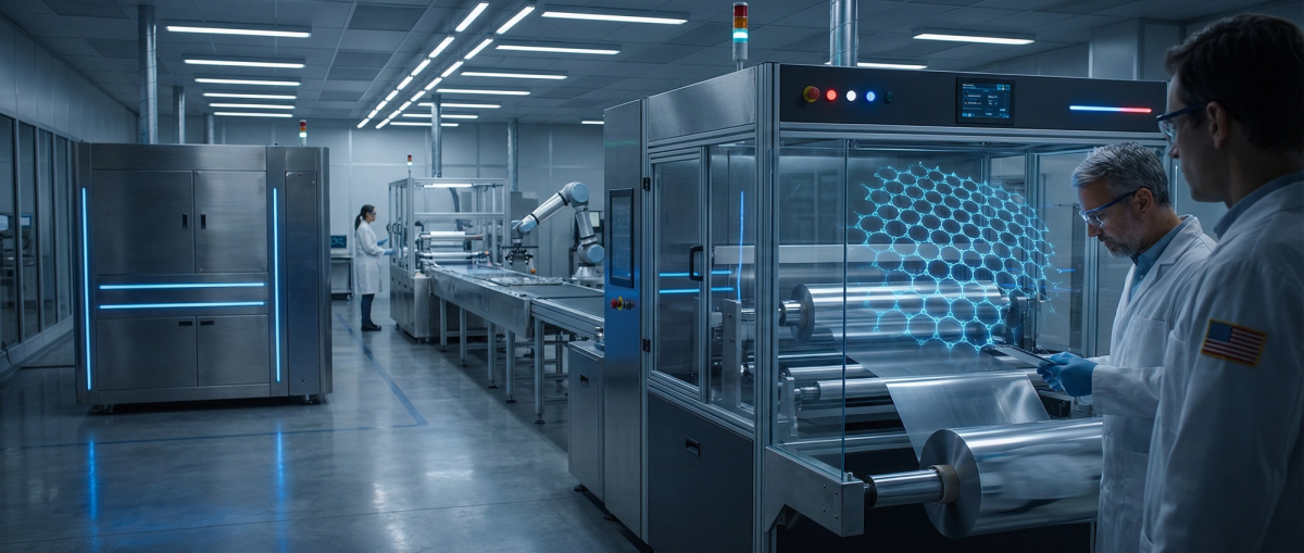
Graphene, a singular atomic plane of sp2-hybridized carbon atoms arranged in a hexagonal lattice, represents the quintessential two-dimensional material whose intrinsic properties are fundamentally dictated by quantum mechanical confinement. This strict planar geometry constrains electron motion to a two-dimensional Dirac point, giving rise to quasiparticles mimicking massless relativistic fermions. This confinement profoundly alters the electronic band structure, manifesting as a linear dispersion relation near the K and K' points of the Brillouin zone, a stark contrast to conventional semiconductors' parabolic characteristics. This unique Dirac physics endows graphene with extraordinary charge carrier dynamics, where electron and hole mobilities routinely exceed 200,000 cm^2/Vs at room temperature, orders of magnitude higher than silicon. The ultra-low intrinsic electrical resistivity, approaching 10^-8 Ohm-meter, positions pristine monolayer graphene as an unparalleled conductor, facilitating near-ballistic transport over micrometer-scale distances. This foundational understanding of its 2D confinement is paramount, as any deviation from atomic monolayer precision or introduction of structural defects severely degrades these intrinsic attributes.
The structural integrity stemming from its sp2 covalent bonding network is equally remarkable. Graphene exhibits an intrinsic tensile strength of approximately 130 GPa, making it the strongest material known, while simultaneously possessing an exceptional Young's modulus of ~1 TPa. This combination of strength and flexibility directly results from its perfectly ordered atomic lattice and robust interatomic forces within the confined 2D plane. Furthermore, its thermal properties are compelling; graphene boasts a thermal conductivity reaching up to 5000 W/mK at room temperature, surpassing diamond or copper, attributable to efficient phonon transport within the single atomic layer. This efficient heat dissipation, coupled with high electrical conductivity, makes it an ideal candidate for thermal management in advanced electronics. The theoretical specific surface area of 2630 m^2/g, a direct outcome of its monolayer nature, also underpins its utility in sensing, catalysis, and energy storage, offering maximal interface for chemical interactions.
Translating these superlative properties into tangible applications at scale presents significant manufacturing challenges, as even minor structural imperfections or unintended doping can drastically alter performance. For instance, precise control over sp2 hybridization and minimizing sp3 defects are critical for preserving high electron mobility. In synthesis routes like chemical vapor deposition (CVD), careful optimization of parameters such as substrate temperature and precursor flow rates is essential to minimize grain boundaries, which act as scattering centers. Similarly, post-processing techniques, including rapid thermal annealing involving localized heating up to 3000K for milliseconds, are sometimes employed to repair lattice defects and enhance crystallinity, thereby restoring optimal electrical characteristics. Beyond electronics, the surface chemistry afforded by graphene's 2D confinement, particularly for graphene oxide (GO) derivatives, enables functionalities like heavy metal adsorption, where GO has demonstrated efficiencies exceeding 79% for lead ion removal from aqueous solutions within short reaction times. The ability to reproducibly produce graphene with specific defect densities, layer counts, and surface chemistries dictates its commercial viability across these diverse high-performance sectors.
Pulsed Electrical Resistive Carbon Heating (PERCH) represents a fundamentally distinct paradigm for graphene synthesis, leveraging ultra-fast thermal transients to transform diverse carbon feedstocks into high-quality graphene. Unlike sustained furnace-based methods, PERCH applies extreme current densities directly to a carbon precursor, inducing rapid Joule heating that can achieve localized temperatures exceeding 3000K within milliseconds. This rapid thermal shock, coupled with the inherent electrical resistivity differences between amorphous carbon and nascent graphitic domains, drives simultaneous graphitization and exfoliation. The instantaneous temperature gradient induces significant thermal expansion and subsequent contraction, mechanically separating graphitic layers while simultaneously annealing structural defects and promoting sp2 hybridization. This process is inherently scalable, capable of processing multi-kilogram batches of inexpensive precursors such as carbon black, graphite flakes, or even certain waste carbons, circumventing the need for solvent-based exfoliation or high-purity crystalline substrates. The precise control over pulse duration, current amplitude, and frequency allows for tailoring the resulting graphene’s morphology, layer count, and defect density, offering a pathway to cost-effective, high-volume graphene powder production.
In contrast, Chemical Vapor Deposition (CVD) epitomizes a surface-mediated growth mechanism, primarily focused on producing large-area, few-layer graphene films on catalytic metal substrates. This process typically involves the decomposition of gaseous carbon precursors, such as methane or acetylene, over heated transition metals like copper or nickel at temperatures ranging from 800°C to 1050°C under controlled atmospheric conditions. The carbon atoms dissolve into the metal lattice, precipitate on the surface, and nucleate into graphene films. While CVD offers unparalleled control over layer number, crystallinity, and domain size for planar applications, its intrinsic limitations for bulk manufacturing are significant. The process is inherently slow, often requiring hours for film growth, and critically dependent on the purity and crystallographic orientation of the substrate. Furthermore, the subsequent transfer of these delicate graphene films from the growth substrate to a target application substrate is a complex, multi-step procedure often introducing defects, tears, and residual contamination from etchants or polymeric supports, substantially impacting yield and performance for many applications.
The operational disparities between PERCH and CVD fundamentally dictate their respective applicability and economic viability for scaling graphene production in the USA. PERCH's rapid, energy-efficient conversion of bulk carbon feedstocks positions it as a superior method for high-volume, low-cost graphene powder synthesis, targeting applications where macroscopic quantities and specific surface functionalities are paramount. For instance, in environmental remediation, PERCH-derived graphene has demonstrated empirical adsorption efficiencies exceeding 79% for heavy metal ions in aqueous solutions, attributable to its high surface area and accessible active sites – a characteristic difficult to achieve economically with CVD films. The energy consumption per unit mass of graphene produced via PERCH is significantly lower, given the localized, transient heating compared to the sustained, high-temperature environment required by CVD reactors. While CVD remains the gold standard for producing pristine, single-layer films for advanced electronics, transparent conductors, and certain sensor applications where direct integration and minimal defects on a specific substrate are non-negotiable, its capital expenditure, slow throughput, and complex transfer steps make it economically prohibitive for the tonnage-scale graphene required for composites, energy storage electrodes, or advanced construction materials. Therefore, the strategic choice between these methodologies hinges on the end-use application, with PERCH offering a robust pathway to industrial-scale bulk graphene manufacturing.
Turbostratic graphene (TG) represents a prevalent structural polymorph within the broader graphene family, distinguished by its lack of long-range ABAB Bernal stacking order along the c-axis. Unlike highly ordered pyrolytic graphite (HOPG) where adjacent graphene layers are precisely registered with a 60-degree rotation and an A-B site offset, TG exhibits arbitrary rotational misorientations between layers, often accompanied by varying interlayer separations. This rotational disorder arises frequently in synthesis pathways such as chemical vapor deposition (CVD) on polycrystalline substrates, certain electrochemical exfoliation methods, and the thermal reduction of graphene oxide (rGO). The presence of such rotational stacking faults fundamentally alters the interlayer van der Waals interactions, resulting in an average interlayer spacing that typically ranges from 0.340 nm to 0.345 nm, measurably larger than the 0.335 nm characteristic of Bernal-stacked graphite. This increased and heterogeneous interplanar distance is a direct crystallographic signature of turbostraticity, influencing subsequent material properties by weakening interlayer electronic coupling and modifying phonon transport pathways.
The crystallographic misalignment inherent to turbostratic graphene profoundly impacts its electronic and thermal transport characteristics, differentiating it from both monolayer graphene and perfectly ordered bulk graphite. Electronically, the rotational disorder disrupts the periodic potential experienced by charge carriers, leading to a decoupling of the Dirac cones from individual layers. This effectively broadens the density of states and can introduce pseudo-gaps, diminishing the high carrier mobility observed in pristine monolayer graphene. Empirical measurements often show in-plane electrical resistivity values for large-area turbostratic films ranging from 1.5 x 10^-5 Ohm-cm to 8.0 x 10^-5 Ohm-cm, a magnitude higher than the 10^-6 Ohm-cm typical for highly ordered graphite. Thermally, the misaligned interfaces act as significant scattering centers for phonons. While monolayer graphene boasts an exceptional thermal conductivity exceeding 3000 W/mK, turbostratic assemblies typically exhibit in-plane thermal conductivities in the range of 500-1000 W/mK, with significantly lower out-of-plane values, due to this enhanced phonon scattering at the rotationally incoherent interfaces. This reduction in both electronic and thermal transport efficiency underscores the critical importance of interlayer alignment in realizing graphene's theoretical performance limits.
Beyond electronic and thermal considerations, the crystallography of turbostratic graphene also dictates its mechanical resilience and chemical reactivity, influencing its suitability for diverse applications. The presence of numerous rotational grain boundaries and dislocation networks within TG structures can act as stress concentrators, potentially reducing the macroscopic tensile strength compared to defect-free monolayer sheets. However, this disorder can also introduce a degree of structural flexibility and increased fracture toughness in certain composite applications. From a chemical perspective, the increased edge-site density and more exposed basal plane regions resulting from the lack of perfect stacking order can enhance reactivity. For example, turbostratic rGO has demonstrated up to 79% heavy metal adsorption efficiency in aqueous solutions due to its higher density of accessible functional groups and adsorption sites compared to pristine graphene. USA manufacturers are actively developing precise synthesis protocols to control or mitigate turbostraticity, employing strategies such as optimized annealing sequences, often involving rapid thermal pulses exceeding 3000K for milliseconds, to induce localized graphitization and reduce defect densities. Conversely, for applications where reactivity or specific surface area are paramount, controlled turbostraticity is intentionally engineered, showcasing a nuanced understanding of how crystallographic parameters can be tailored for application-specific performance.
The transition from laboratory-scale graphene synthesis to industrial-grade production presents formidable challenges, primarily revolving around process control, material consistency, and yield economics. Top-down exfoliation methods, such as liquid-phase exfoliation (LPE) from graphite, offer high throughput potential but struggle with precise control over flake dimensions, layer number, and defect density. While sonication-assisted LPE can achieve high aspect ratio flakes, maintaining a narrow distribution of lateral dimensions (e.g., 500 nm to 5 µm) and a consistent monolayer content (e.g., >80%) across multi-kilogram batches remains a significant hurdle. Batch-to-batch variability in oxygen functionalization (e.g., 5-15 wt% oxygen for graphene oxide) and resulting changes in electrical resistivity (e.g., 10^-2 to 10^0 Ohm.cm after reduction) directly impact downstream application performance. Conversely, bottom-up approaches like Chemical Vapor Deposition (CVD) offer superior control over film quality, producing large-area, high-purity monolayer graphene with electron mobilities exceeding 2000 cm^2/Vs on copper foils. However, the multi-step transfer process from catalytic substrate to target material is inherently prone to defects, tears, and polymer residue, which can reduce carrier mobility by an order of magnitude and increase sheet resistance from ~30 Ohm/sq to >100 Ohm/sq. Scaling CVD requires colossal reactor volumes, high-purity precursor gases, and energy-intensive processing, including substrate annealing often exceeding 1000°C, making cost-effective, high-volume production a substantial capital expenditure barrier for US manufacturers.
Beyond synthesis, the commercial integration of graphene is hampered by the persistent "graphene paradox"—the difficulty of translating superlative laboratory properties into real-world applications at economically viable scales. End-users demand not just "graphene" but application-specific, tailored materials with guaranteed performance metrics. For instance, achieving a critical percolation threshold in polymer composites requires highly dispersible graphene with specific surface chemistry and aspect ratios to enhance mechanical properties by >30% or electrical conductivity by several orders of magnitude, yet preventing agglomeration during compounding remains a complex rheological challenge. The thermal management sector, eyeing graphene's ~2000 W/mK intrinsic thermal conductivity, often finds that industrial-grade few-layer graphene composites struggle to surpass 500 W/mK due to phonon scattering at interfaces and high defect concentrations. Furthermore, integrating graphene into existing manufacturing lines often necessitates significant process re-engineering. For example, incorporating graphene into battery electrodes requires meticulous control over slurry rheology and coating uniformity to avoid localized hot spots or premature degradation, demanding precise control over particle size and surface charge, adding substantial processing costs and extending time-to-market.
A critical impediment to widespread commercial adoption is the absence of universally accepted, comprehensive standardization protocols for graphene characterization and performance validation. While techniques like Raman spectroscopy, X-ray Photoelectron Spectroscopy (XPS), and Atomic Force Microscopy (AFM) are standard in research, their interpretation and reporting vary widely across manufacturers, leading to a lack of comparability and trust in material specifications. This ambiguity complicates procurement decisions and risk assessments for industrial integrators. For example, a "monolayer" claim might encompass significant bilayer or multilayer inclusions, altering electrical resistivity from 10^-6 Ohm.cm to 10^-3 Ohm.cm. Regulatory frameworks also lag, particularly concerning environmental impact and long-term health implications. Robust life cycle assessments (LCAs) are nascent, and comprehensive toxicology data for various graphene derivatives, especially regarding aerosolized nanoparticles or leachates, are still being compiled. While certain functionalized graphene oxide variants demonstrate promising heavy metal adsorption efficiencies (e.g., 79% for lead ions), the economic viability hinges on cost-effective regeneration and safe disposal, which are not yet fully optimized at scale. The overall cost-performance ratio against established materials—even with graphene's superior theoretical properties—remains a significant economic barrier, requiring substantial market education and de-risking investments from manufacturers to demonstrate clear, quantifiable value propositions.
The economic feasibility of industrial-scale graphene production within the USA is undergoing a critical transition from laboratory synthesis to high-volume manufacturing, driven by advancements in both bottom-up and top-down methodologies. While initial synthesis costs were prohibitive for broad market penetration, contemporary techniques like roll-to-roll chemical vapor deposition (CVD) and optimized electrochemical exfoliation are significantly reducing the cost per unit area or mass. For instance, advanced CVD systems are now achieving monolayer graphene growth over meter-scale substrates with defect densities below 10^9 defects/cm^2, utilizing precursor gases such as methane and hydrogen with flow rates precisely controlled to minimize waste, thereby enhancing material yield and reducing operational expenditure. Similarly, flash Joule heating techniques, capable of converting various carbon feedstocks into turbostratic graphene, demonstrate remarkable energy efficiency, achieving localized temperatures exceeding 3000K via rapid thermal pulses lasting mere milliseconds. This rapid thermal processing minimizes reactor residence time and energy consumption per unit of graphene produced, pushing the cost profile closer to industrial economic thresholds required for bulk applications in composites and energy storage. The inherent capital intensity of these advanced manufacturing processes, coupled with the need for rigorous quality control to ensure batch-to-batch consistency in parameters like electrical resistivity (e.g., target sub-10^-6 Ohmcm for few-layer films) and crystallite size, necessitates substantial investment, which USA-based manufacturers are uniquely positioned to leverage through robust venture capital ecosystems and strategic government funding initiatives.
The USA-made manufacturing advantage for graphene is fundamentally rooted in a confluence of factors including unparalleled research and development infrastructure, stringent quality control standards, and robust intellectual property protection. Unlike regions where the emphasis might solely be on cost minimization, US manufacturers prioritize the production of high-specification graphene tailored for demanding applications in aerospace, defense, advanced microelectronics, and medical devices. This focus translates into superior material purity (e.g., metallic impurity levels consistently below 5 ppm), precise control over layer count, and functionalization capabilities that are critical for achieving specific performance enhancements. For example, in advanced thermal management, US-produced graphene films are engineered to exhibit anisotropic thermal conductivities exceeding 2000 W/mK in-plane, a metric crucial for high-power electronics. Furthermore, the ability to rapidly iterate on synthesis parameters and integrate advanced characterization techniques directly into the production line ensures that graphene products meet exacting customer specifications, reducing downstream integration risks. The domestic supply chain resilience offered by USA-based production also mitigates geopolitical vulnerabilities and logistical complexities, ensuring a consistent and reliable supply of critical advanced materials for strategic industries.
Economic feasibility for graphene extends beyond the manufacturing cost per kilogram; it encompasses the total value proposition derived from its integration into end products, particularly where its unique properties enable performance breakthroughs or system-level cost reductions. In applications such as lightweight structural composites for automotive and aerospace, the incorporation of functionalized graphene nanoplatelets at concentrations as low as 0.5 wt% has demonstrated tensile strength enhancements exceeding 30% and fracture toughness improvements of 25%, leading to significant fuel efficiency gains and extended service life. For environmental remediation, graphene oxide membranes engineered with precise pore sizes and surface chemistries have achieved heavy metal adsorption efficiencies of 79% for Pb2+ ions in wastewater treatment, offering a highly effective and regenerable solution that outperforms traditional filtration media. These performance metrics translate directly into a compelling return on investment for end-users, justifying the premium associated with high-quality, domestically manufactured graphene. The USA’s strong regulatory framework for material safety and environmental compliance further solidifies the market position of US-made graphene, ensuring that innovations are not only technologically superior but also sustainable and responsible, fostering long-term market trust and adoption.
Graphene's trajectory extends beyond current prototypes, pushing material science into unattainable realms. Its fundamental quantum mechanical properties, such as Dirac fermion behavior and robust ballistic transport at ambient temperatures, position it as a critical enabler for next-generation computing architectures, including topological quantum bits and ultra-fast terahertz communication systems. Graphene-based spintronics, leveraging weak spin-orbit coupling and long spin diffusion lengths, promises to revolutionize data storage and processing, yielding picosecond-speed devices. Its unparalleled strength-to-weight ratio (exceeding 130 GPa tensile strength) and intrinsic thermal stability render it indispensable for advanced aerospace composites and extreme environment sensors, demanding operational integrity from cryogenic lows to transient 3000K thermal pulses. Functionalized graphene's ability to detect single-atom variations or femtomolar analytes opens avenues for medical diagnostics and environmental monitoring with unprecedented specificity and millisecond response. These attributes translate directly into high-value B2B applications in defense, space exploration, and high-frequency electronics, contingent upon consistently high-quality, scalable graphene production.
The immediate and mid-term commercialization landscape for graphene is characterized by disruptive potential across industrial sectors, driven by empirically validated performance enhancements. In energy storage, graphene-enhanced supercapacitors demonstrate specific capacitances exceeding 500 F/g, exhibiting over 99% capacitance retention across 10,000 cycles, and enabling full charge in seconds, surpassing conventional battery chemistries in power density. Thermal management leverages graphene's exceptional in-plane thermal conductivity, approaching 5000 W/mK for pristine samples, facilitating heat dissipation from high-power electronics at densities up to 1000 W/cm^2, crucial for data centers and electric vehicle battery packs. Environmental remediation offers significant opportunity; graphene oxide membranes achieve sub-nanometer filtration, removing pharmaceutical residues and microplastics, while functionalized graphene adsorbents demonstrate up to 79% heavy metal (Pb/Cd) adsorption efficiency. In advanced coatings and composites, minimal graphene loadings (typically less than 1 wt%) impart substantial improvements in mechanical strength (e.g., 30% increase in tensile strength), electrical conductivity, and corrosion resistance, extending product lifecycles and reducing maintenance costs across automotive, marine, and infrastructure applications.
Realizing these future horizons and high-value applications hinges critically on establishing robust, scalable manufacturing processes delivering industrial quantities of graphene with consistent quality and tailored properties. US-based manufacturers lead in advanced production methodologies, including large-area chemical vapor deposition (CVD) for electronic-grade films at square-meter scales, and proprietary electrochemical exfoliation techniques yielding high-purity few-layer graphene powders at hundreds of kilograms per month. Critical to market adoption is stringent quality control, with characterization standards encompassing Raman spectroscopy metrics (e.g., D/G ratio below 0.2), sheet resistance uniformity (e.g., <5% variation across large substrates), and defect density analysis. Integration of graphene into complex systems, from 3D-printed meta-materials to flexible bio-electronic interfaces, demands high-quality input material and sophisticated post-processing. As demand for high-performance, cost-effective graphene proliferates across strategic sectors like defense and medical devices, resilient, domestically controlled supply chains become paramount. This ensures critical material input security and fosters innovation within the US industrial ecosystem, driving costs towards targets like sub-$100/kg for select graphene grades and accelerating commercial reality.
Serious about B2B integration? Test our premium Pulsed Electrical Resistive Carbon Heating turbostratic graphene in your lab. 100g sample packs available now.
Explore More
A practical market-first review of the easiest graphene applications to launch today, based on five real product categories with clear adoption paths and customer ROI.

Discover how graphene-reinforced PEEK plastic improves mechanical strength, wear resistance, and thermal stability for high-performance engineering applications.

A technical deep dive into how graphene can improve ionic transport, interface stability, and manufacturable cell architecture in solid-state sodium batteries.