Electronics & Photonics
Graphene in Photonic Chips: Why a One-Atom-Thick Material Matters for the Future of Light-Based Computing
Photonic chips are often described as the next major platform for high-speed communications, sensing, and computation. Instead of relying only on moving electrons through resistive metal interconnects, photonic integrated circuits manipulate photons through waveguides, resonators, modulators, detectors, and couplers fabricated on a chip-scale platform. This offers several compelling advantages: extremely high bandwidth, reduced electromagnetic interference, and the ability to multiplex large numbers of optical channels in parallel. But photonic systems also face a persistent problem. Light is exceptionally fast and low-loss for transport, yet it is often difficult to control efficiently on chip without using materials that add size, power, fabrication complexity, or speed limitations.
That is where graphene becomes deeply interesting.
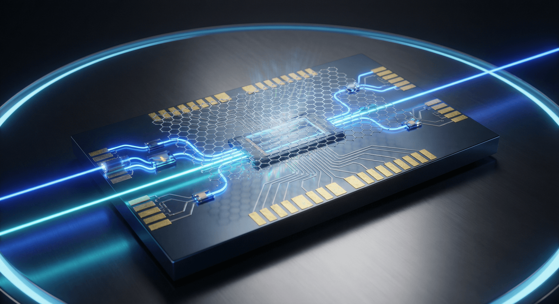
Graphene is a two-dimensional sheet of carbon atoms arranged in a hexagonal lattice, famous for its exceptional electrical conductivity, mechanical strength, thermal transport, optical tunability, and compatibility with a broad range of substrates. In electronic devices, graphene has long been discussed as a high-mobility material. In photonics, however, its value is arguably even more strategic. Graphene interacts with light over an extremely broad spectral range, from visible to infrared and terahertz frequencies. More importantly, its optical response can be tuned electrically. That combination makes graphene a strong candidate for enabling compact, fast, energy-efficient components inside photonic chips.
When people talk about “graphene and light” in an integrated chip context, the real opportunity is not simply that graphene can sit next to optical hardware. The opportunity is that graphene can become an active functional layer that changes how light is generated, modulated, detected, absorbed, switched, and thermally managed on chip. In short, graphene can help photonic chips become more compact, more reconfigurable, and more multifunctional.
Why Conventional Photonic Platforms Need Better Active Materials
Silicon photonics is the most mature integrated photonics platform today because it leverages semiconductor manufacturing infrastructure. Silicon waveguides, splitters, ring resonators, and grating couplers can be fabricated at scale with strong reproducibility. However, silicon is not ideal for every photonic function. For example, silicon’s indirect bandgap makes light emission inefficient. Electro-optic effects in silicon are comparatively limited, often forcing designers to rely on carrier injection or depletion mechanisms that can increase footprint and complexity. Thermal tuning is widely used, but it consumes static power and can introduce thermal crosstalk.
Other materials such as indium phosphide, silicon nitride, lithium niobate, phase-change materials, and III-V heterostructures all solve parts of this problem, but each brings its own manufacturing tradeoffs, process complexity, or cost structure. What the field still wants is a material that can be integrated as a thin functional layer, gives strong optical tunability, responds quickly, and does not require an entirely separate fabrication ecosystem.
Graphene fits that profile unusually well.
Because it is atomically thin, graphene can be transferred onto existing photonic architectures without requiring the entire chip to be built from graphene. This is important. In practice, graphene is not replacing the silicon photonic platform; it is augmenting it. A silicon or silicon nitride waveguide can provide the low-loss optical pathway, while graphene acts as an ultrathin active interface. Through electrostatic gating, optical pumping, or thermal interaction, graphene can modify absorption, refractive behavior, and carrier dynamics in a way that is useful for device engineering.
Graphene as an Optical Modulator Material
One of the most promising uses of graphene in photonic chips is optical modulation. A modulator encodes information onto light by changing intensity, phase, or polarization. This function is central to optical interconnects, communications, and emerging photonic computing architectures.
Graphene is attractive here because its optical absorption and conductivity can be tuned by shifting the Fermi level. In practical terms, applying an electrical bias can alter how graphene interacts with light traveling in a nearby waveguide. This makes it possible to build electro-absorption modulators and electro-refractive modulators that are compact and potentially very fast.
Compared with bulk semiconductor modulators, graphene-based modulators can offer several theoretical and demonstrated advantages:
- broadband operation, especially in telecom and mid-infrared bands,
- small device footprints due to strong light-matter interaction in integrated structures,
- potentially high-speed response because of graphene’s fast carrier dynamics,
- compatibility with hybrid integration onto existing photonic platforms.
The key engineering challenge is overcoming graphene’s atomic thinness. A single graphene layer does not interact strongly with free-space light over long distances simply because there is so little material. On-chip photonics solves this by forcing light to propagate in tightly confined waveguide modes that overlap with the graphene sheet over a defined interaction length. Designers can then optimize waveguide geometry, cladding, and electrode structures to maximize modulation depth while limiting insertion loss.
This is why graphene matters specifically in photonic chips rather than just in optical materials research. The chip architecture provides the confinement and integration environment that allows graphene’s tunable optical physics to become technologically useful.
Photodetection and Broadband Light Sensing
Graphene is also compelling for photodetectors. Most conventional photodetectors are optimized for a relatively narrow spectral region determined by a semiconductor bandgap. Graphene, in contrast, has no conventional bandgap in pristine form and can absorb light across a very wide spectral range. That opens the door to broadband detectors covering visible, telecom, infrared, and potentially terahertz regimes.
In an integrated photonic chip, graphene photodetectors can be positioned directly on or near waveguides so that guided optical modes are absorbed by the graphene layer. Detection mechanisms can include photoconductive, photovoltaic, photothermoelectric, or bolometric effects, depending on device design. This diversity is useful because different chip applications need different tradeoffs among speed, sensitivity, dark current, and wavelength range.
For example, a telecom interconnect chip may prioritize bandwidth and CMOS-compatibility, while a spectroscopy chip may prioritize broadband response. A graphene-based detector platform has the flexibility to be engineered for either case. In sensing applications, graphene’s surface sensitivity also adds another dimension: the same material system can support both optical detection and interaction with the surrounding environment, potentially enabling compact optoelectronic biosensors or chemical sensors.
Reconfigurable Photonics and Tunable Optical Elements
Another major trend in photonic chip development is reconfigurability. Future photonic systems are increasingly expected to behave less like static circuits and more like programmable optical fabrics. That means switches, tunable filters, variable attenuators, phase shifters, and adaptive routing elements are becoming more important.
Graphene offers a credible path here because its optical and electrical properties are dynamically controllable. Instead of relying only on thermal heaters to shift resonances in ring resonators or Mach-Zehnder interferometers, engineers can integrate graphene to create electrically tunable elements. This could reduce power consumption and improve switching speed compared with purely thermo-optic approaches.
In practical architectures, graphene can be coupled to:
- ring resonators for tunable resonance control,
- interferometers for phase or amplitude modulation,
- plasmonic structures for strong field confinement,
- metasurfaces and hybrid optical stacks for custom spectral responses.
The combination of graphene with resonant photonic structures is especially powerful. Resonators enhance local optical fields, allowing stronger interaction with the graphene layer than would otherwise occur. This can improve device efficiency, though it must be balanced against bandwidth limitations and fabrication tolerances.
Graphene for Photonic Chips Beyond Communications
It would be a mistake to frame graphene photonics only as a telecom story. The opportunity is broader.
Photonic chips are increasingly relevant in AI accelerators, lidar, quantum optics, spectroscopy, environmental sensing, medical diagnostics, and compact imaging. In many of these areas, graphene provides one or more useful traits that traditional materials do not combine in a single platform.
In optical computing and AI hardware, graphene-based modulators and detectors could contribute to lower-energy optical data movement between cores or memory domains. In sensing, graphene’s broadband behavior and strong surface interaction can support miniaturized spectroscopic devices. In mid-infrared photonics, where many molecules have strong absorption fingerprints, graphene can support active device concepts that are hard to implement efficiently with silicon alone. In terahertz systems, graphene’s tunable conductivity becomes even more interesting for modulators, antennas, and detectors.
There is also an underappreciated systems-level advantage: graphene is multifunctional. A material that can contribute to optical modulation, detection, thermal spreading, transparent conduction, and sensing is valuable because it reduces the need for a different specialty material at every device layer. Over time, that could simplify heterogeneous photonic integration strategies.
Thermal Management and Device Reliability
Photonic chips are not purely optical systems. They are also thermal systems. Laser sources, electrical drivers, heaters, detectors, and surrounding electronics all generate heat. Temperature drift changes refractive indices, shifts resonances, and reduces system stability. High-performance photonic packaging increasingly depends on effective heat management.
Graphene’s in-plane thermal conductivity has made it famous in thermal interface and spreading discussions. While thermal performance in real devices depends strongly on interfaces, defects, stacking, and encapsulation, graphene and graphene-derived films can still play a useful role in local heat spreading around active photonic regions. Better thermal transport does not just improve reliability; it can improve wavelength stability, reduce control overhead, and support denser integration.
For photonic chips with tightly packed active elements, this matters. The closer components are placed, the more thermal crosstalk becomes a design constraint. Materials that help localize or dissipate heat more intelligently may become enabling, not just beneficial.
Manufacturing Challenges That Still Need to Be Solved
The case for graphene in photonic chips is strong, but it is not automatic. There are real barriers between promising lab devices and scalable commercial adoption.
First, material quality and transfer consistency remain critical. Photonic devices are sensitive to contamination, wrinkles, cracks, residue, and interfacial disorder. A graphene layer with uneven doping or imperfect placement can introduce loss and variability that erase the theoretical advantage.
Second, contact engineering and gate-stack design are not trivial. To use graphene effectively in modulators or detectors, one must build reliable electrical interfaces that do not ruin optical performance. This creates a coupled design problem across optics, electronics, and fabrication.
Third, integration flow matters. A photonic foundry process must be able to incorporate graphene without destroying yield, contaminating lines, or adding too much process overhead. For graphene to become mainstream in photonic chips, it must fit into economically realistic manufacturing paths.
Fourth, device benchmarking needs to mature. It is not enough for a graphene modulator to work; it must outperform or complement established options in a clear way. Metrics such as insertion loss, modulation efficiency, drive voltage, energy per bit, speed, footprint, wavelength range, and long-term reliability all matter. Industry adoption will depend on system-level value, not only material novelty.
Why the Long-Term Outlook Is Still Strong
Despite these challenges, the strategic logic remains compelling. The future of advanced photonic chips will likely be heterogeneous. No single material system will dominate every function. Instead, chip designers will combine low-loss passive waveguide platforms with specialized active materials layered or bonded where needed.
Graphene is extremely well positioned for this future because it is not trying to replace the entire photonic stack. It is trying to make the stack smarter.
A one-atom-thick conductive optical interface that can be electrically tuned, integrated onto existing waveguides, respond over a wide spectral range, and potentially improve both active optoelectronic performance and thermal behavior is exactly the kind of enabling material that heterogeneous photonics needs. The companies and research groups that solve the integration and repeatability problem may gain a serious advantage in next-generation modulators, detectors, reconfigurable optical circuits, and compact sensing systems.
Final Perspective
Graphene in photonic chips is not hype because graphene is fashionable. It matters because photonics needs better active material interfaces, and graphene offers an unusually rich set of optical, electrical, and thermal properties in an ultrathin form factor.
If silicon photonics gave the industry a scalable optical highway, graphene may help provide the adaptive control layer that makes that highway more useful. By enabling broadband modulation, integrated detection, tunable optical response, compact reconfigurability, and better thermal engineering, graphene has the potential to become one of the most important hybrid materials in the evolution of photonic integrated circuits.
The commercial winners will not just be the groups that prove graphene works in a lab. They will be the ones that make graphene reliable, manufacturable, and system-relevant inside real photonic chips. That is where the material stops being interesting and starts being valuable.