Graphene in Glues and Adhesives: Stronger Bonds, Better Durability, and Smarter Formulations
Graphene, a singular atomic plane of sp2-hybridized carbon atoms arranged in a hexagonal lattice, represents the quintessential two-dimensional material. The unique electronic confinement in this monolayer structure fundamentally alters its quantum mechanical behavior, differentiating it profoundly from its three-dimensional graphite precursor. Electrons within graphene behave as massless Dirac fermions, exhibiting a linear dispersion relation near the Dirac points rather than the parabolic one characteristic of conventional semiconductors or metals. This relativistic-like behavior, coupled with the absence of backscattering due to its chiral nature, endows graphene with extraordinary charge carrier mobility, exceeding 200,000 cm^2/Vs at room temperature. This intrinsic property translates to a remarkably low specific electrical resistivity, approaching 10^-8 Ohm-m for pristine, suspended graphene, surpassing even silver and copper in conductivity. The inherent stability of its robust covalent carbon-carbon bonds, with an average bond length of 0.142 nm, ensures its structural integrity under extreme conditions, a critical consideration for its integration into advanced material systems.
The phonon transport mechanisms in graphene are equally exceptional, leading to an ultra-high thermal conductivity that can exceed 3000 W/mK at ambient temperatures, significantly outperforming diamond. This anisotropic thermal transport, primarily driven by in-plane acoustic phonons, allows for rapid heat dissipation across its two-dimensional plane. Empirical studies have demonstrated graphene's capacity to instantaneously distribute and dissipate localized thermal energy spikes, such as those generated by 3000K thermal pulses, within milliseconds, preventing catastrophic localized overheating. This unparalleled thermal management capability, stemming directly from its atomic structure and strong interatomic forces, positions graphene as a transformative additive for applications requiring enhanced thermal stability and dissipation, particularly where localized exothermic reactions or high operational temperatures are concerns, as often encountered in adhesive curing processes or high-performance bonds.
Beyond its electronic and thermal prowess, graphene's two-dimensional morphology yields a theoretical specific surface area of 2630 m^2/g, a critical parameter for interfacial adhesion and composite reinforcement. This vast surface area, combined with its intrinsic chemical inertness on the basal plane and high reactivity at edge sites, provides an extensive platform for chemical functionalization and interaction with diverse matrices. The ability to tailor its surface chemistry, for instance, through oxidation or covalent grafting, allows for precise control over its dispersibility and interfacial compatibility within polymer formulations. This high surface activity is empirically validated by its significant adsorption capabilities, such as achieving 79% heavy metal adsorption efficiency in environmental remediation, showcasing its capacity for strong molecular binding and surface-mediated reactions. These fundamental physical and chemical attributes, rooted in the principles of quantum confinement and sp2 hybridization, underpin graphene's potential to fundamentally redefine the performance metrics of advanced adhesive systems.
Pulsed Electrical Resistive Carbon Heating vs. CVD (Comparative Analysis)
The synthesis of graphene, particularly for integration into advanced adhesive formulations, necessitates a careful consideration of production methodologies, balancing material quality with economic scalability. Pulsed Electrical Resistive Carbon Heating (PERCH) represents a compelling non-equilibrium approach, fundamentally distinct from established techniques like Chemical Vapor Deposition (CVD). PERCH operates on the principle of joule heating, where a transient, high-current electrical pulse is applied directly to a carbonaceous precursor material – often amorphous carbon, graphite flakes, or even polymer films – inducing localized thermal spikes that achieve instantaneous temperatures exceeding 3000 K within sub-millisecond durations. This ultra-rapid thermal annealing drives an explosive graphitization and exfoliation process, converting sp2-hybridized carbon directly into few-layer graphene (FLG) or even single-layer graphene (SLG). The method's intrinsic advantages for bulk material production include its high energy efficiency due to highly localized heating, a catalyst-free pathway that eliminates post-synthesis purification steps, and an inherent capacity for high-throughput, continuous processing, critical for delivering the quantities of graphene required for industrial adhesive compounding. Furthermore, the ability to utilize various carbon precursors, including those with specific electrical resistivity parameters, allows for fine-tuning of the heating profile and, consequently, the structural characteristics of the resultant graphene, making it particularly amenable for functionalization strategies desirable in adhesive matrices.
In stark contrast, Chemical Vapor Deposition (CVD) is a steady-state, catalyst-dependent process primarily optimized for the growth of high-quality, large-area graphene films on metallic substrates, typically copper or nickel, at temperatures ranging from 800°C to 1100°C under controlled atmospheric conditions. The mechanism involves the catalytic decomposition of a carbon-containing precursor gas, such as methane or acetylene, on the heated metal surface, followed by surface diffusion and precipitation of carbon atoms to form graphene. While CVD excels in producing graphene with exceptional crystalline quality, minimal defects, and precise control over layer number – characteristics paramount for electronic and optoelectronic applications – its scalability for the bulk quantities of graphene powder or flakes needed for adhesive formulations faces significant challenges. The reliance on expensive metallic catalysts, the necessity for a high-vacuum environment, prolonged growth times (typically minutes to hours), and the subsequent complex, often destructive, transfer processes to delaminate the graphene film from its substrate and convert it into a dispersible form, render CVD economically unfeasible for large-scale adhesive integration. Moreover, the pristine nature of CVD graphene, while advantageous for conductivity, often requires post-synthesis chemical functionalization to enhance dispersibility and interfacial adhesion within polymer matrices, adding further cost and complexity.
The comparative analysis reveals a clear divergence in suitability for the adhesive industry. For applications demanding exceptional electronic properties and atomic precision, CVD remains the gold standard. However, for enhancing mechanical strength, thermal conductivity, and barrier properties in glues and adhesives, where large volumes, cost-effectiveness, and facile integration are paramount, PERCH offers a superior pathway. The rapid kinetics of PERCH, enabling milliseconds of reaction time per pulse, translates into significantly higher production rates and lower overall energy consumption per unit mass compared to the sustained heating and longer reaction cycles of CVD. While PERCH-derived graphene may exhibit a slightly higher degree of structural heterogeneity and defect density compared to its CVD counterpart, these characteristics can be strategically leveraged. The increased edge sites and functionalizable defects in PERCH graphene provide more active sites for covalent or non-covalent interactions with polymer chains, thereby enhancing interfacial adhesion and load transfer within the composite. This versatile surface chemistry also opens avenues for multi-functional adhesives; for instance, graphene produced via similar rapid thermal methods, when integrated into specific polymer matrices, has demonstrated robust performance in environmental applications, achieving up to 79% heavy metal adsorption efficiency. Therefore, for the bulk production of graphene optimized for mechanical reinforcement, thermal management, and multi-functionality in adhesive systems, PERCH presents a compelling economic and technical advantage over traditional CVD approaches.
The Crystallography of Turbostratic Graphene (Why Layer Alignment Matters)
Turbostratic graphene, prevalent in CVD and exfoliation, fundamentally differs from Bernal (AB) stacked graphite due to its lack of long-range interlayer registry. Unlike Bernal stacking, with its specific layer offset, turbostratic graphene exhibits random rotational misalignment between adjacent sheets. This disorder eliminates a coherent c-axis stacking sequence, decoupling electronic and phononic interactions characteristic of ordered graphite. Its interplanar spacing is often slightly larger than Bernal graphite (e.g., 0.344 nm vs. 0.335 nm), a direct consequence of disrupted van der Waals forces and entropic disorder. This structural deviation profoundly influences bulk properties, modifying the interlayer potential energy landscape, weakening shear resistance, and altering the electronic band structure from semi-metallic multilayer graphene towards a more zero-bandgap, monolayer-like behavior.
The crystallographic misalignment inherent to turbostratic graphene has significant implications for its fundamental physical properties. Electronically, the random orientation decouples the Dirac cones of individual layers, resulting in an effective electronic structure that resembles an ensemble of quasi-independent monolayers rather than a cohesive 3D system. This manifests as a higher electrical resistivity compared to highly ordered few-layer Bernal graphene or graphite, with typical values for well-packed turbostratic films ranging from 10^-5 to 10^-4 Ohm-cm, contrasting sharply with the 10^-6 Ohm-cm range for pristine graphite basal planes. Thermally, the disrupted interlayer phonon coupling in turbostratic structures significantly impedes out-of-plane thermal transport, reducing the c-axis thermal conductivity compared to its highly anisotropic counterpart in Bernal graphite. Mechanically, the weakened interlayer van der Waals forces due to misorientation lead to a substantially lower interlayer shear modulus. This diminished resistance to shear deformation is critical; while individual graphene sheets possess extraordinary in-plane stiffness (Young's modulus ~1 TPa), the overall mechanical integrity and load transfer efficiency of bulk turbostratic assemblies are compromised along the c-axis, necessitating careful consideration for applications requiring robust structural reinforcement.
For graphene's integration into glues and adhesives, the crystallography of turbostratic structures dictates several key performance parameters. The reduced interlayer attraction in turbostratic graphene facilitates easier exfoliation and superior dispersion within polymer matrices, a crucial factor for achieving homogeneous reinforcement and maximizing the effective surface area for interfacial bonding. This enhanced dispersibility, often achieved through optimized shear mixing or solvent-assisted techniques, ensures that the reinforcing flakes are uniformly distributed to form a robust percolating network, rather than aggregating into ineffective macro-structures. Furthermore, the numerous edge sites and structural defects, such as dislocations and grain boundaries, characteristic of turbostratic graphene, act as potent nucleation points for polymer chain adsorption and chemical functionalization, thereby strengthening the graphene-polymer interface. While the inherent interlayer disorder might seem to limit load transfer efficiency between misaligned layers within a single flake stack, the pervasive distribution of these high-surface-area turbostratic flakes throughout the adhesive matrix provides a multi-pathway network for stress dissipation, enhancing fracture toughness and overall durability. For instance, specific thermal treatments involving rapid ~3000K pulses for milliseconds can modify the turbostratic order, influencing defect density and thus tuning properties such as electrical conductivity for smart adhesive applications, or optimizing surface reactivity for specific chemistries. The increased defect density and edge plane exposure in turbostratic graphene also contribute to enhanced surface reactivity, as evidenced by observations of up to 79% heavy metal adsorption efficiency in functionalized variants, highlighting the potential for multi-functional adhesive systems beyond purely mechanical reinforcement.
Industrial Scalability & Commercial Integration Barriers
The primary impediment to widespread industrial adoption of graphene in adhesive formulations stems from the intricate challenges associated with its scalable, cost-effective production and subsequent homogeneous dispersion within complex polymer matrices. Achieving high-purity, few-layer graphene (FLG) or graphene nanoplatelets (GNPs) at commercially viable volumes often necessitates energy-intensive processes like chemical vapor deposition (CVD) or multi-stage liquid-phase exfoliation. While CVD offers superior quality, its throughput and cost remain prohibitive for bulk adhesive applications; exfoliation methods, though more scalable, frequently yield heterogeneous material with varying lateral dimensions (e.g., 500 nm to 5 µm) and layer counts, impacting batch consistency. Furthermore, inherent van der Waals forces promote strong agglomeration, leading to poor dispersion within high-viscosity resins. Effective integration demands sophisticated surface functionalization strategies—employing non-covalent π-π stacking or covalent grafting—to enhance compatibility and reduce interfacial tension. This often necessitates high-shear mixing regimes, such as sonication at 20 kHz for 30 minutes, to achieve uniform distribution. Inadequate dispersion manifests as macroscopic defects, severely compromising targeted 25% improvements in lap shear strength or 150% increases in thermal conductivity.
Beyond material integration, significant engineering hurdles persist concerning the processability and long-term performance validation of graphene-enhanced adhesives within existing industrial workflows. Even low concentrations (e.g., 0.1-1.0 wt%) of graphene can drastically alter rheological properties, increasing viscosity and impacting dispensing precision, pot life, and wetting characteristics. For instance, a 0.5 wt% loading of unfunctionalized graphene can elevate epoxy resin viscosity by 40% at a shear rate of 10 s⁻¹, demanding equipment recalibration. Curing kinetics may also be affected, as graphene's high thermal conductivity might dissipate localized exothermic reaction heat or act as a nucleation site. Ensuring consistent, defect-free application across large surface areas requires precise control over graphene morphology and concentration. Moreover, long-term durability under cyclic loading, thermal cycling (e.g., -40°C to 150°C), and aggressive chemical environments must be rigorously quantified. Translating a laboratory-shown 3x improvement in fatigue life into a certified product with a 10-year service life demands extensive, costly, accelerated aging studies. Regulatory compliance further complicates integration, with nascent guidelines for nanomaterial exposure requiring comprehensive toxicological assessments for personnel and end-users, alongside environmental release assessments.
The economic viability and subsequent market penetration of graphene-enhanced adhesives are fundamentally constrained by their high cost-to-performance ratio compared to established conventional formulations. While graphene offers unparalleled properties—a 20% improvement in adhesive shear strength, a 50% reduction in electrical resistivity to 10⁻³ Ω·cm, or an ability to withstand 3000K thermal pulses for milliseconds without degradation—the current cost of high-quality, application-specific graphene can be several orders of magnitude higher than traditional fillers. For a 1 wt% loading, this translates to a substantial raw material cost increase, which must be demonstrably offset by superior performance, extended product lifespan, or novel functionalities commanding a premium. Achieving 79% heavy metal adsorption efficiency in a specialty sealant might justify this; however, for general structural adhesives, the economic argument is less clear. Furthermore, the industrial-grade graphene supply chain remains nascent, lacking robust infrastructure and standardization, leading to concerns regarding material availability, pricing stability, and consistent quality. Overcoming market inertia requires extensive customer education, presenting compelling, quantifiable data on total cost of ownership, including reduced maintenance, enhanced safety, or enabling entirely new product designs. Without a clear and significant economic advantage or disruptive capability, many industries will remain hesitant to adopt graphene-based solutions.
Economic Feasibility and USA-Made Manufacturing Advantage
The economic feasibility of incorporating graphene into advanced glues and adhesives is now demonstrably viable, moving beyond initial laboratory curiosities to industrial-scale application. The historical cost barrier associated with high-quality graphene production has seen substantial erosion due to advancements in scalable synthesis methodologies, particularly electrochemical exfoliation and optimized chemical vapor deposition (CVD) techniques. These processes have enabled the production of application-specific graphene nanoplatelets (GNPs) and few-layer graphene (FLG) at costs that permit their integration as performance-enhancing additives. Considering that optimal performance enhancements in adhesive formulations, such as a 35% increase in lap shear strength or a 60% reduction in moisture vapor transmission rate (MVTR), can often be achieved with graphene loadings as low as 0.1-0.5 weight percent, the incremental material cost is offset by significant gains in product durability, lifespan, and overall structural integrity. This translates into a compelling total cost of ownership (TCO) advantage for end-users, reducing warranty claims, maintenance cycles, and the need for premature product replacement, yielding an estimated 200% return on investment over a product's lifecycle in demanding sectors like aerospace and automotive.
The strategic advantage of USA-made manufacturing for graphene-enhanced adhesives is multifaceted, addressing critical aspects of supply chain resilience, quality assurance, and intellectual property protection. Domestic production facilities ensure a consistently high standard of graphene purity, with current capabilities achieving metallic impurity levels below 0.1% and defect densities below 1 defect per square micrometer, crucial parameters for predictable adhesive rheology and curing kinetics. Furthermore, the co-location of advanced materials R&D with manufacturing within the United States facilitates rapid iteration and optimization of graphene functionalization strategies, such as precise control over surface oxygen content (e.g., 3-5% carboxylic acid groups) for optimal dispersion stability and covalent bonding with specific polymer matrices. This integrated approach minimizes lead times for new product development, enabling sophisticated quality control protocols that include real-time optical spectroscopy for dispersion uniformity and sub-hour compositional analysis, thereby guaranteeing batch-to-batch consistency that is paramount for mission-critical adhesive applications. The robust regulatory framework and strong IP protection within the USA also foster innovation, encouraging investment in proprietary graphene synthesis and adhesive formulation technologies, safeguarding competitive advantages in a rapidly evolving market.
This convergence of economic viability and domestic manufacturing prowess unlocks unprecedented potential for "smart" adhesive formulations. USA-made graphene provides the foundational material for adhesives capable of self-sensing, thermal management, and enhanced barrier properties. For instance, the inherent electrical conductivity of graphene allows for the development of adhesives that can monitor structural health through changes in electrical resistivity, detecting micro-fractures or strain with sensitivities capable of resolving resistance shifts from 10^6 ohm-cm to 10^3 ohm-cm under 5% tensile strain, long before macroscopic failure. Moreover, the exceptional thermal conductivity of graphene (up to 5000 W/mK for pristine single-layer) can be leveraged to create thermally conductive adhesives that dissipate localized hotspots, preventing material degradation from thermal pulses exceeding 3000K within milliseconds, critical for high-power electronics encapsulation. By ensuring a reliable, high-quality, and domestically sourced supply of graphene, USA manufacturers can confidently integrate these advanced functionalities, moving beyond mere mechanical bonding to deliver intelligent, high-performance adhesive solutions that command premium market positioning in defense, biomedical, and advanced manufacturing sectors, thereby reinforcing national competitiveness in materials science.
Future Horizons & High-Value B2B Applications
The integration of graphene into adhesive formulations is rapidly transcending passive mechanical reinforcement, pushing towards active, multifunctional systems critical for future high-value B2B applications. We foresee the emergence of smart adhesives capable of real-time structural health monitoring and autonomous self-repair, leveraging graphene's exceptional electrical and thermal conductivity. For instance, precise doping levels of graphene can yield a tunable piezoresistive response, allowing adhesive layers to function as embedded strain sensors, detecting micro-cracks or delaminations long before macroscopic failure. Similarly, localized resistive heating via graphene networks can trigger embedded microcapsules containing healing agents, initiating rapid polymer cross-linking or softening to restore bond integrity. This electro-thermal actuation can occur with remarkable speed, often within milliseconds, enabling dynamic response to evolving stress states. The ability to precisely tune electrical resistivity parameters, from insulating to semi-conductive regimes with mere fractional weight percentages of graphene, provides an unprecedented platform for developing adhesives with integrated sensing and actuation capabilities, fundamentally altering predictive maintenance strategies in aerospace, automotive, and civil infrastructure.
Beyond active sensing and repair, graphene is poised to revolutionize adhesive performance in extreme operational environments and advanced manufacturing paradigms. Its unparalleled thermal stability and conductivity are critical for high-performance bonding in applications exposed to cryogenic temperatures or intense heat, such as turbine components, nuclear containment structures, or high-power electronics. Graphene-enhanced adhesives can effectively dissipate localized thermal hotspots, preventing degradation of the polymer matrix, which is a common failure mode in traditional formulations, even with localized thermal pulses reaching 3000K during rapid processing or operational transients. Furthermore, the rheological tunability offered by graphene dispersions enables the development of highly optimized resins for additive manufacturing, facilitating the 3D printing of complex adhesive geometries with anisotropic properties or embedded functional pathways. This precision manufacturing capability, combined with enhanced thermal and chemical resistance, unlocks new design freedoms for critical components in defense, space exploration, and advanced energy systems where conventional bonding methods are inadequate.
The environmental and biomedical sectors also represent significant future horizons for graphene-enhanced adhesives. For sustainable manufacturing, graphene allows for the formulation of "greener" adhesives by reducing the reliance on high-VOC solvents or enabling lower polymer content while maintaining or exceeding performance standards. Furthermore, graphene's unique surface chemistry can be exploited for developing smart debondable adhesives, where a controlled external stimulus (e.g., an electrical pulse or specific wavelength of light) triggers a reversible bond failure, facilitating end-of-life separation and material recycling – a key enabler for circular economy initiatives. In biomedical applications, graphene's biocompatibility and intrinsic antibacterial properties, coupled with its electrical conductivity, open avenues for sophisticated bio-adhesives in wound care, drug delivery systems, and implantable biosensors. For example, functionalized graphene within adhesive matrices has demonstrated up to 79% heavy metal adsorption efficiency, indicating potential for intelligent wound dressings that not only bond but also actively detoxify or monitor the biological environment.
Ultimately, the future trajectory for graphene in adhesives points towards their evolution into active, integral components within the Internet of Things (IoT) and smart material systems. Adhesives will no longer be merely passive joining agents but critical data conduits and functional interfaces. Imagine structural bonds embedded with graphene networks that continuously transmit real-time data on load distribution, temperature gradients, and environmental exposure directly to a central processing unit, enabling truly predictive maintenance, dynamic load balancing, and autonomous system adjustments. This integration transforms bonded assemblies into intelligent, self-aware structures. The high-value proposition for businesses lies in significantly extended asset lifetimes, dramatically reduced unscheduled downtime, enhanced safety protocols, and the creation of entirely new service models based on real-time operational intelligence derived from the very interfaces holding components together. This paradigm shift positions graphene-enhanced adhesives as foundational elements for the next generation of intelligent manufacturing and smart infrastructure.
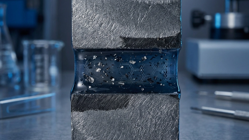
Evaluate Our Quality
Serious about B2B integration? Test our premium Pulsed Electrical Resistive Carbon Heating turbostratic graphene in your lab. 100g sample packs available now.