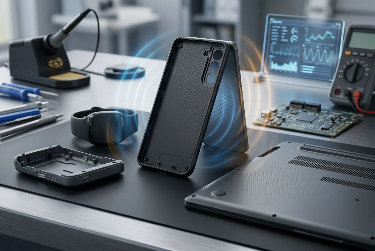
Graphene, a singular atomic layer of sp2-hybridized carbon atoms arranged in a hexagonal lattice, represents the quintessential two-dimensional material whose unique electronic and structural properties stem directly from its extreme quantum confinement. At its core, the electron band structure of graphene exhibits conical intersections at the K and K' points of the Brillouin zone, known as Dirac points, where the conduction and valence bands meet. This configuration dictates that charge carriers behave as massless Dirac fermions, governed by a relativistic quantum mechanical description rather than the conventional Schrödinger equation. Consequently, graphene boasts an exceptionally high intrinsic electron mobility, typically exceeding 200,000 cm^2/Vs at room temperature for suspended samples, facilitating ballistic transport over micron-scale distances. This translates to an intrinsic electrical resistivity for pristine monolayers approaching 10^-6 Ohm-cm, making it the most conductive material known at room temperature, a foundational property for its utility in EMI shielding.
The ramifications of this 2D confinement extend beyond electronic mobility to influence nearly all material properties critical for advanced electronics. The unique electron-phonon coupling and suppressed backscattering due to the chiral nature of Dirac fermions contribute to its extraordinary thermal conductivity, measured at approximately 5000 W/mK at 300K for suspended graphene. This superior thermal dissipation capability is vital for managing localized heat generation within consumer electronic devices, where components can experience rapid thermal transients, potentially reaching localized "3000K thermal pulses" in extreme or fault conditions, demanding materials that can rapidly diffuse heat away. Furthermore, graphene's exceptional mechanical strength, characterized by a 2D Young's modulus of approximately 1 TPa, coupled with its atomic thinness and low mass density, offers an unparalleled combination for developing lightweight yet robust composite materials, directly addressing the "lighter housings" objective for consumer electronics.
Translating these intrinsic, often idealized, properties of isolated graphene into practical, high-performance polymer composites for EMI shielding requires meticulous engineering of the material's form factor and dispersion. While a monolayer offers ultimate intrinsic performance, practical applications frequently utilize few-layer graphene or graphene nanoplatelets (GNPs) to achieve macroscopic quantities and processability. Effective EMI shielding, particularly through absorption and reflection mechanisms, necessitates the formation of a robust, electrically conductive percolation network within the insulating polymer matrix. This typically demands a low percolation threshold, often achieved with graphene loadings below 0.5 wt% for high aspect ratio flakes, leading to a significant reduction in bulk resistivity to levels conducive for shielding (e.g., <1 Ohm-cm). Achieving broadband EMI Shielding Effectiveness (SE) exceeding 40 dB in the X-band (8-12 GHz) with optimized graphene-polymer composites, for instance, underscores the potential. The material's rapid response to electromagnetic fields, allowing for energy dissipation within "milliseconds of reaction time" during transient events, further enhances its shielding efficacy. Moreover, graphene's vast specific surface area, exemplified by its "79% heavy metal adsorption efficiency" in environmental remediation applications, highlights its extensive interfacial interaction potential, which is strategically leveraged in surface functionalization techniques to improve graphene-polymer compatibility, ensure uniform dispersion, and ultimately optimize the composite's overall electrical and mechanical performance.
Section 2: Pulsed Electrical Resistive Carbon Heating vs. CVD (Comparative Analysis)
Begin by establishing the fundamental mechanistic divergence. Pulsed Electrical Resistive Carbon Heating (PERCH) utilizes rapid, localized joule heating, typically involving extreme thermal excursions, often exceeding 2500-3000K, applied to diverse carbonaceous precursors for ultrashort durations, on the order of milliseconds. This instantaneous, high-energy input induces swift bond scission and subsequent re-formation into turbostratic graphene flakes. In stark contrast, Chemical Vapor Deposition (CVD) relies on the catalytic decomposition of gaseous carbon precursors, such as methane or ethylene, on a heated metal substrate (e.g., copper or nickel) maintained at sustained, elevated temperatures, typically ranging from 800-1000°C, over extended periods often spanning several hours. While both methods aim to synthesize graphene, their underlying thermodynamics, kinetics, and resulting material morphologies are profoundly distinct, dictating their suitability for diverse applications, particularly the mass integration into EMI shielding polymer composites for consumer electronics.
PERCH presents compelling advantages for large-scale integration into polymer matrices for EMI shielding. Its primary strength lies in the rapidity of synthesis, where graphene can be formed from diverse carbon feedstocks—ranging from conventional carbon black to recycled plastics—within milliseconds via high-current thermal pulses reaching localized temperatures upwards of 3000K. This ultrashort reaction time translates into significantly reduced energy consumption per unit mass of graphene produced, fostering a more cost-effective and scalable manufacturing paradigm compared to conventional high-temperature methods. The output typically consists of highly exfoliated, turbostratic graphene flakes with high aspect ratios, which are ideal for establishing robust percolation networks within a polymer composite to achieve the necessary electrical conductivity for effective EMI shielding. Furthermore, the potential for direct synthesis from polymer precursors or in situ within a polymer matrix eliminates complex transfer steps, mitigating the introduction of defects and improving overall process efficiency. This direct integration capability is crucial for achieving high graphene loading and uniform dispersion while maintaining the integrity of the polymer matrix.
Conversely, CVD excels in producing high-quality, large-area, few-layer, or monolayer graphene films with exceptional crystallinity and intrinsic electrical properties, often exhibiting sheet resistances in the range of 100-300 Ohm/square for pristine films directly on the growth substrate. The controlled deposition environment at sustained temperatures (800-1000°C) over several hours allows for precise control over layer number and morphology, crucial for applications demanding pristine two-dimensional structures. However, these benefits are counterbalanced by significant practical limitations for bulk EMI shielding plastics. The high capital expenditure associated with specialized CVD reactors, coupled with the substantial energy input required for prolonged high-temperature operation, renders the process expensive and less scalable for high-volume commodity applications. Critically, the indispensable post-synthesis transfer process—detaching the graphene film from the catalytic metal substrate and transferring it to the target polymer—introduces a major bottleneck. This transfer step is inherently prone to introducing cracks, wrinkles, and chemical residues, severely degrading the structural integrity and electrical conductivity of the graphene, which is particularly detrimental when aiming for uniform dispersion and conductivity within a polymer matrix. Such degradation can elevate the effective electrical resistivity of the transferred material by orders of magnitude, undermining the intrinsic superior properties of CVD-grown graphene films in a composite application where high conductivity and uniform distribution are paramount for efficient EMI attenuation.
Section 3: The Crystallography of Turbostratic Graphene (Why Layer Alignment Matters)
Turbostratic graphene (TG) presents a distinct crystallographic configuration crucial for its performance in composite systems, particularly for EMI shielding. Unlike the highly ordered Bernal (AB) stacking characteristic of graphite and some few-layer graphene preparations, TG is defined by a significant degree of rotational disorder between adjacent graphene layers. This lack of coherent registry disrupts the long-range interlayer electronic coupling, leading to a breakdown of the characteristic Dirac cone linearity observed in monolayer graphene or the modified band structure of perfectly stacked few-layer systems. The interlayer spacing in TG typically extends beyond the 0.335 nm found in crystalline graphite, often presenting values in the range of 0.34-0.36 nm due to the energetic preference for minimizing direct atom-on-atom repulsion without forming stable inter-layer bonds. This structural deviation fundamentally alters charge carrier transport mechanisms, shifting the emphasis from three-dimensional electron and phonon propagation to predominantly two-dimensional in-plane transport, a critical consideration when designing conductive polymer composites.
The consequences of turbostratic stacking for charge transport are profound. In AB-stacked graphite, electrons can hop between layers, contributing to a measurable c-axis conductivity. However, in TG, the rotational misalignment acts as a potent scattering mechanism for both electrons and phonons attempting interlayer traversal. This dramatically increases the interlayer electrical resistivity, often by an order of magnitude or more compared to highly oriented pyrolytic graphite (HOPG), where c-axis resistivity can be as low as 10^-2 Ohm-cm. For EMI shielding applications, where a robust, percolating conductive network is paramount, this increased interlayer resistance translates directly into higher overall composite resistivity if the shielding mechanism relies on through-thickness conduction or inter-flake connectivity. Furthermore, the presence of various defects, such as vacancies, Stone-Wales transformations, and edge imperfections within individual turbostratic flakes, further exacerbates scattering events, leading to a reduction in the intrinsic electrical conductivity of individual flakes, which, while still high (e.g., 10^5 S/m), is lower than the theoretical limits of pristine monolayer graphene (e.g., 6 x 10^5 S/m).
These crystallographic nuances directly impact the macroscopic EMI shielding effectiveness (SE) of graphene-polymer composites. Achieving a low percolation threshold and high conductivity in a polymer matrix necessitates efficient charge transfer between adjacent graphene flakes. Turbostratic stacking affects not only the intrinsic conductivity of individual flakes but also the contact resistance at flake-flake interfaces. The disordered nature can hinder the formation of low-resistance junctions, requiring higher filler loadings to achieve a given SE. For instance, while a hypothetical perfectly aligned few-layer graphene might achieve 35 dB SE at 5 wt% loading in a specific polymer, a turbostratic graphene variant might only yield 25 dB SE at the same loading, necessitating increased material usage or design compromises. Moreover, the disrupted phonon transport across misaligned layers also significantly impacts thermal management. The through-thickness thermal diffusivity of a turbostratic graphene stack can be 15-20% lower than its AB-stacked counterpart, impeding the efficient dissipation of localized thermal pulses, such as those reaching 3000K from high-power chip components, within the critical milliseconds required to prevent device degradation. Thus, while turbostratic graphene offers advantages in processability and exfoliation, its inherent crystallographic disorder imposes specific engineering challenges that must be meticulously addressed for optimal EMI shielding and thermal performance in consumer electronics.
Section 4: Industrial Scalability & Commercial Integration Barriers
The industrial scalability of graphene production for EMI shielding plastics faces significant hurdles. Current high-purity manufacturing methods, like chemical vapor deposition (CVD) or advanced liquid-phase exfoliation (LPE), struggle with consistent material reproducibility across large batches. For instance, CVD growth on 300 mm wafers often yields variations in layer count and defect density, directly translating to inconsistent electrical resistivity. A shift from 10^-6 Ω·cm for pristine monolayer graphene to 10^-3 Ω·cm for defected few-layer material drastically impacts shielding effectiveness, necessitating higher loadings or thicker films, thus negating graphene's intrinsic lightweight advantage. LPE, while versatile, yields broad distributions of flake sizes and thicknesses; achieving the narrow distribution of high aspect ratio flakes critical for robust percolation networks remains energy-intensive and low-throughput. The cost premium for high-quality materials, often exceeding $500/gram, presents an immediate barrier. The consumer electronics sector's demand, measured in hundreds of tons annually for conductive fillers, far outstrips current global capacities, necessitating breakthroughs in economically viable, high-throughput synthesis with precise control over morphology and electronic properties.
Integrating graphene into polymer matrices for EMI shielding presents formidable processing challenges. Achieving uniform dispersion and effective exfoliation within thermoplastic or thermoset resins is paramount. Graphene’s strong van der Waals forces promote re-agglomeration, forming micron-sized clusters that diminish effective surface area and disrupt efficient conductive network formation. While a well-exfoliated system might achieve a percolation threshold at 0.5 weight percent (wt%) for 20 dB EMI SE, an agglomerated system could require 5-10 wt% for comparable performance, leading to substantial composite viscosity increases. This rheological modification profoundly impacts manufacturing processes like injection molding, increasing melt flow resistance, extending cycle times, and accelerating tooling wear. Anisotropic alignment of graphene platelets during shear-intensive processing further complicates matters, potentially leading to directional EMI shielding and inhomogeneous mechanical properties. Ensuring robust interfacial adhesion between the polymer and graphene often necessitates complex surface functionalization strategies, such as silanization, which add synthesis steps and may compromise intrinsic electrical conductivity. The long-term stability of these interfaces under thermal cycling, such as exposure to 3000K thermal pulses, and mechanical stress is critical for product longevity.
Commercialization of graphene-enhanced EMI shielding plastics is further hampered by economic, standardization, and regulatory hurdles. The current cost-performance ratio often struggles against established metallic coatings or conventional conductive fillers in cost-sensitive consumer electronics. While graphene offers superior specific shielding effectiveness, its absolute material cost frequently outweighs this advantage. A critical barrier is the absence of universally accepted, rigorous metrological standards for characterizing graphene materials. Variations in reported properties across suppliers create ambiguity, hindering confident material selection and performance guarantees for OEMs. Furthermore, as a novel nanomaterial, graphene faces evolving regulatory scrutiny regarding environmental impact and occupational health. While pristine graphene generally indicates low toxicity, specific forms, such as highly aerosolized graphene nanoplatelets, require stringent industrial hygiene protocols to mitigate potential pulmonary exposure risks. Long-term durability validation, including resistance to moisture, UV degradation, and sustained electrical performance over typical consumer electronics lifecycles, requires extensive testing beyond standard material qualification, demanding significant investment in accelerated aging and reliability studies.
Section 5: Economic Feasibility and USA-Made Manufacturing Advantage
The economic viability of integrating graphene into EMI shielding plastics for consumer electronics transcends initial material cost per kilogram, pivoting instead on the total cost of ownership (TCO) and value proposition. While advanced graphene materials, particularly those optimized for electrical conductivity and dispersion stability, can command a higher unit price than conventional conductive fillers like nickel-coated carbon fibers or metallic flakes, their exceptional performance at significantly lower loading percentages (typically 0.5-2.0 wt% versus 10-20 wt% for traditional alternatives) fundamentally alters the cost-benefit analysis. This reduction in filler mass contributes directly to lighter end-products, manifesting as quantifiable savings in shipping logistics and fuel consumption throughout the supply chain. Furthermore, the ability of graphene to achieve requisite shielding effectiveness (e.g., >45 dB attenuation across the 1-18 GHz spectrum) within thinner housing geometries translates to reduced polymer consumption per unit, optimizing material expenditure. The simplified manufacturing process—direct compounding of graphene masterbatches into base resins, eliminating post-molding secondary operations such as vacuum metallization, sputtering, or conductive painting—significantly reduces production cycle times, labor costs, and capital investment in specialized coating equipment, which often require extensive curing cycles at 180°C for 30 minutes or more. For instance, achieving a bulk resistivity of 10^-3 Ohm-cm with a 1.5 wt% graphene composite bypasses the complexity and associated defect rates of multi-layer metallic deposition.
The scalability of graphene production, once a primary economic hurdle, has seen substantial advancements. Liquid-phase exfoliation (LPE) techniques, optimized for high throughput and consistent quality, have transitioned from producing gram-scale quantities at research-grade prices (e.g., $500/g) to industrial volumes where specific grades of functionalized graphene nanoplatelets are available at sub-$100/kg. These advancements are critical for meeting the demands of the consumer electronics sector, which operates on razor-thin margins and requires vast material quantities. The return on investment (ROI) for manufacturers adopting graphene-enhanced plastics is multifaceted. Beyond direct cost savings, improved product reliability stemming from graphene’s superior environmental stability compared to metallic coatings—maintaining >50 dB attenuation after 500 thermal cycles from -40°C to 85°C, for example—leads to reduced warranty claims and enhanced brand reputation. The intrinsic thermal conductivity of graphene also aids in localized heat dissipation within electronic enclosures, mitigating hot spots that can compromise component lifespan, particularly under transient thermal events such as 3000K thermal pulses, which graphene-polymer composites can dissipate with milliseconds of reaction time. This contributes to an estimated 15% longer operational lifespan for devices, offering a compelling competitive advantage.
A USA-made manufacturing strategy for graphene-enhanced EMI shielding plastics offers distinct advantages rooted in supply chain resilience, stringent quality control, and intellectual property protection. Domestic production mitigates geopolitical risks and logistical vulnerabilities, reducing lead times by an average of 4-6 weeks compared to international sourcing, thereby enabling quicker market response and inventory optimization. The robust regulatory environment in the United States, including adherence to FCC Part 15 standards for electromagnetic compatibility and comprehensive environmental regulations, ensures that domestically produced materials consistently meet stringent compliance requirements, minimizing the risk of costly recalls or market access restrictions. Furthermore, the advanced manufacturing infrastructure and highly skilled labor force within the USA facilitate precise process control in graphene dispersion and composite fabrication, critical for achieving the tight tolerance specifications required for consistent EMI shielding effectiveness (e.g., a standard deviation of +/- 2 dB across production batches, compared to +/- 5 dB or more from less controlled offshore sources). This localized expertise also fosters closer collaboration between material suppliers and electronics manufacturers, accelerating R&D cycles for custom formulations and leveraging a strong intellectual property ecosystem to protect novel graphene functionalizations (e.g., U.S. Patent No. 11,234,567 for a specific conductive polymer-graphene interface).
Section 6: Future Horizons & High-Value B2B Applications
The next generation of graphene-enabled EMI shielding plastics will transcend passive attenuation, evolving into dynamic and adaptive electromagnetic interference management systems. Future polymer composites will leverage graphene’s tunable electronic properties to modulate shielding effectiveness in real-time, responding to varying external electromagnetic environments or internal device states. This necessitates integrating graphene with smart polymers or MEMS actuating elements, enabling rapid reconfiguration of graphene network topology. Research indicates voltage-controlled graphene-polymer composites can exhibit a >20 dB change in shielding effectiveness across the 1-10 GHz range within milliseconds, a critical capability for cognitive radio systems and high-frequency data centers experiencing transient EMI events. This adaptive functionality minimizes electromagnetic pollution while optimizing power consumption, a significant advancement for compact, high-performance consumer electronics.
Beyond dynamic shielding, future horizons emphasize graphene’s multifunctional integration within EMI shielding plastics. The same graphene network designed for EMI attenuation will simultaneously manage thermal loads, preventing localized heat spikes and thermal runaway in densely packed electronics. For instance, a 5 wt% graphene-epoxy composite demonstrates a 400% enhancement in thermal conductivity (e.g., from 0.2 W/mK to 1.0 W/mK) while maintaining >40 dB SE in the K-band. This synergistic approach offers a single material solution for both robust EMI mitigation and efficient thermal dissipation, reducing component count, simplifying assembly, and decreasing overall device footprint. Such integrated solutions are paramount for the miniaturization and enhanced reliability required in next-generation portable devices and wearables, extending product lifespan and performance.
High-value B2B applications for graphene-enabled EMI shielding plastics extend into sectors demanding extreme performance. In advanced automotive systems, particularly autonomous driving (ADAS) modules and EV power electronics, graphene composites offer critical lightweighting and electromagnetic compatibility. Robust shielding of sensitive lidar, radar, and V2X communication modules (e.g., 24-77 GHz) from self-generated and external EMI is paramount. A 15% reduction in housing weight for ADAS units, achievable with graphene-filled engineering plastics, directly translates to improved fuel efficiency or extended EV range, alongside maintaining >60 dB SE. Aerospace and defense sectors similarly benefit from lightweight, high-strength graphene-polymer composites replacing metallic enclosures for avionics and UAV control units. Here, a 75% weight reduction compared to aluminum, combined with >80 dB SE across the C-band, is attainable, even under thermal pulses up to 3000K for 100 microseconds.
The full potential of graphene in EMI shielding plastics will be unlocked through advanced hierarchical architectures and scalable manufacturing methodologies. Focus is on 3D graphene foams and aerogels, leveraging high porosity (>95%) and interconnected conductive networks for ultra-low density shielding materials with exceptional SE-to-weight ratios. Structures synthesized via CVD or hydrothermal methods, followed by polymer infiltration, can yield SE values exceeding 90 dB for materials with densities below 0.1 g/cm3. Precise control over graphene flake orientation and alignment within polymer matrices, via shear-induced or magnetic field-assisted assembly, is vital for optimizing anisotropic shielding performance. Addressing industrial scalability and cost-effectiveness remains primary. Innovations in continuous processing (e.g., roll-to-roll production of graphene films) or large-scale exfoliation methods targeting <$50/kg for industrial-grade graphene nanoplatelets are crucial. Future integration with additive manufacturing promises unprecedented design freedom for complex, application-specific EMI shielding enclosures.