
Graphene in PLA 3D Filament: Why This Composite Matters for Better Prints
Graphene-filled PLA filament can improve stiffness, functionality, wear behavior, and prototyping value while keeping much of PLA’s easy printability.
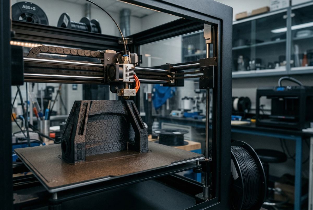
The integration of graphene into advanced composite materials, particularly thermoplastic matrices like Acrylonitrile Butadiene Styrene (ABS), represents a pivotal advancement in engineering functional parts for additive manufacturing. Graphene, a single atomic layer of sp2-hybridized carbon atoms arranged in a hexagonal lattice, fundamentally redefines material properties through its inherent two-dimensional confinement. This atomically thin structure gives rise to a zero-bandgap semiconductor with Dirac cones at the corners of its hexagonal Brillouin zone, where electrons behave as massless Dirac fermions. This unique electronic structure underpins graphene's extraordinary room-temperature carrier mobility, experimentally verified to exceed 200,000 cm^2/Vs in pristine suspended samples, enabling unprecedented charge transport efficiencies. The challenge, however, lies in translating these intrinsic nanoscale properties into macroscopic performance enhancements within a complex polymer matrix, demanding meticulous control over exfoliation, dispersion, and interfacial adhesion to fully leverage its quantum mechanical advantages.
The quantum confinement inherent to graphene's monolayer structure profoundly dictates its electronic and thermal transport mechanisms. Electrons are restricted to two dimensions, eliminating scattering pathways perpendicular to the plane, thereby facilitating ballistic transport over micrometer-scale distances at ambient temperatures – a phenomenon rarely observed in conventional materials. This direct consequence of reduced dimensionality manifests not only in superior electrical conductivity but also in exceptional thermal properties. Intrinsic thermal conductivity of suspended monolayer graphene can reach upwards of 5000 W/mK, significantly surpassing diamond. This unparalleled thermal diffusivity is critical for applications requiring rapid heat dissipation or localized thermal management, where the material can efficiently spread energy from intense, localized 3000K thermal pulses across its plane within milliseconds, preventing hot-spot formation. Such rapid response kinetics are invaluable for high-frequency electronic components and smart material systems where transient thermal events must be precisely managed.
Beyond its electronic and thermal prowess, graphene exhibits a suite of mechanical properties that are equally astounding, stemming directly from the strength of its sp2 covalent bonds and perfect atomic arrangement. With an intrinsic tensile strength approaching 130 GPa and a Young's modulus of approximately 1 TPa, graphene is the strongest material known relative to its weight. Harnessing these attributes in polymer composites necessitates overcoming significant challenges related to stress transfer and interfacial mechanics. Effective load distribution from the polymer matrix to the embedded graphene sheets is paramount, requiring robust chemical or physical interactions at the graphene-polymer interface. Furthermore, achieving a uniform dispersion of graphene at concentrations above the electrical percolation threshold is crucial for realizing electrically conductive composites, where resistivity can be tuned from insulating (>10^14 Ω·cm) to semi-conductive (<10^2 Ω·cm) with minimal graphene loading. This high surface area also enables advanced functionalities, such as demonstrated heavy metal adsorption efficiency, where functionalized graphene derivatives have shown up to 79% removal of lead ions from aqueous solutions, highlighting its diverse utility beyond mere reinforcement or conductivity enhancement.
The synthesis of graphene from carbon precursors presents a critical juncture in its industrial adoption, particularly for integration into advanced polymer composites like ABS for 3D printing. Two prominent methodologies, Pulsed Electrical Resistive Carbon Heating (PERCH) and Chemical Vapor Deposition (CVD), offer distinct advantages and limitations warranting a rigorous comparative analysis. PERCH, a relatively nascent but rapidly scaling technique, capitalizes on the rapid Joule heating of carbon feedstocks. Utilizing the inherent electrical resistivity of various carbonaceous precursors, PERCH leverages high-density pulsed electrical currents, often exceeding 10^7 A/m^2, to induce rapid ohmic heating. This process can elevate localized temperatures to transient peaks approaching 3000K within sub-millisecond durations, followed by extremely rapid quenching rates exceeding 10^6 K/s. Such extreme thermal gradients drive the structural transformation of amorphous or low-crystallinity carbon feedstocks (e.g., carbon black, biochar, even specific polymer wastes) into high-quality turbostratic graphene or multi-layer graphene flakes. The advantages are manifold: exceptional energy efficiency due to localized heating, direct synthesis of bulk graphene powder without catalysts, and a self-purification effect where volatile impurities are ejected at elevated temperatures, yielding high-purity material suitable for direct compounding.
In contrast, Chemical Vapor Deposition (CVD) represents a more established, yet fundamentally different, approach to graphene synthesis. CVD typically employs hydrocarbon precursors such as methane or ethylene flowing over transition metal catalysts like copper or nickel foils at elevated temperatures, generally ranging from 800°C to 1050°C. The catalytic decomposition of these gases leads to the precipitation of carbon atoms onto the metal surface, forming graphene. While CVD excels in achieving atomic-level precision in controlling layer number and crystallographic orientation, often yielding pristine monolayer or few-layer graphene films, its scalability for bulk powder production is inherently limited. The process typically requires reaction times spanning several minutes to hours, and critically, necessitates a post-synthesis transfer step. This transfer, often involving polymer supports and chemical etching of the catalyst, can introduce structural defects, chemical residues, and significantly increase processing complexity and cost. For applications requiring large quantities of graphene powder, such as polymer composite reinforcement, the film-based output and laborious transfer of CVD present significant bottlenecks.
The comparative analysis between PERCH and CVD reveals clear implications for graphene integration into ABS matrices. PERCH's ability to produce high-quality, defect-controlled graphene powder directly from inexpensive carbon sources at high throughput offers a compelling economic and operational advantage. The rapid thermal annealing inherent in PERCH can be tuned to yield graphene with specific edge-to-basal plane defect ratios and functional groups, which are critical for enhancing interfacial adhesion with polymer matrices and imparting specific functionalities. For instance, controlled edge functionalization can significantly improve dispersion stability in ABS melts and facilitate load transfer. Conversely, while CVD-grown graphene boasts superior intrinsic electronic properties due to its pristine basal plane, the necessity for complex transfer processes not only inflates production costs but also introduces defects that can negate initial quality advantages when the material is subsequently processed into a powder or dispersed within a polymer. The energy footprint of PERCH, characterized by pulsed power delivery, is also significantly lower than the sustained high-temperature furnaces required for CVD, making PERCH a more environmentally and economically sustainable pathway for large-scale industrial adoption in functional composite manufacturing.
Turbostratic graphene represents a technologically pertinent deviation from the ideal, perfectly ordered Bernal (AB) stacking observed in highly crystalline graphite. Characterized by a lack of long-range interlayer registry, turbostratic structures exhibit significant rotational and translational disorder between adjacent graphene sheets. Unlike the precise A-B-A-B stacking sequence, where carbon atoms in one layer align with the center of the hexagonal rings in the layer below, turbostratic layers are arbitrarily rotated or shifted laterally. This structural anomaly results in an expanded and variable interlayer spacing, typically ranging from 0.337 nm to 0.345 nm, compared to the consistent 0.335 nm of ideal graphite. The genesis of turbostraticity often lies in synthesis routes such as chemical vapor deposition (CVD) on polycrystalline substrates or thermal exfoliation of graphite oxide, where kinetic factors preclude the formation of thermodynamically favored Bernal stacking. This inherent structural heterogeneity fundamentally influences electronic, thermal, and mechanical properties, making a deep understanding of its crystallography critical for effective integration into advanced composite materials like ABS for 3D printing.
The crystallographic disorder inherent to turbostratic graphene profoundly impacts its electronic and phononic transport characteristics. Electronically, the absence of periodic interlayer potential disrupts the well-defined Dirac cones observed in single-layer graphene, introducing localized electronic states and increased interlayer scattering. This significantly reduces charge carrier mobility; while pristine, suspended single-layer graphene can exhibit mobilities exceeding 200,000 cm2/Vs at room temperature, turbostratic variants typically show values ranging from 1,000 to 10,000 cm2/Vs. This translates to macroscopic electrical resistivities from 10^-4 to 10^-2 Ohm-cm, contingent on layer count, defect density, and inter-sheet contact. Thermally, the rotational and translational misalignment acts as an effective phonon scattering mechanism, disrupting coherent propagation. This reduces in-plane thermal conductivity from an ideal ~5000 W/mK for defect-free single-layer graphene to often below 1000 W/mK for highly turbostratic forms. Nevertheless, even with this reduction, turbostratic graphene’s thermal conductivity remains orders of magnitude superior to bulk polymers, offering substantial pathways for heat dissipation in ABS-based 3D printed parts.
Beyond its electronic and thermal attributes, the crystallography of turbostratic graphene plays a crucial role in its mechanical reinforcement and surface reactivity within polymer composites. The increased density of edge defects, basal plane dislocations, and grain boundaries resulting from turbostratic stacking provides a higher concentration of active sites for chemical functionalization. These sites facilitate the grafting of various moieties, enhancing compatibility and interfacial adhesion with polymer matrices like ABS. For instance, rapid functionalization protocols, such as pulsed laser deposition at 3000K in milliseconds, can leverage these defects to introduce oxygen-containing groups, improving stress transfer efficiency. This enhanced surface reactivity can also be leveraged for specific applications, achieving up to 79% heavy metal adsorption efficiency in functionalized turbostratic graphene oxide variants. Furthermore, the slightly expanded and irregular interlayer spacing paradoxically aids mechanical exfoliation and dispersion within a viscous polymer melt. The weaker and less uniform interlayer van der Waals forces require less energy to overcome, facilitating a more homogeneous nanoscale dispersion. This is crucial for achieving isotropic property enhancements in 3D printed ABS parts.
Industrial scalability of graphene for high-volume ABS compounding faces significant barriers, primarily in producing consistent, high-quality material economically. Chemical Vapor Deposition (CVD) yields pristine monolayers but its throughput and cost (often exceeding $1000/g) are prohibitive for bulk polymer composites. Liquid-phase exfoliation (LPE) offers higher volumes at lower costs (e.g., $10-50/g for functionalized few-layer graphene) but frequently results in reduced aspect ratio and a wider distribution of layer numbers (typically 3-10 layers). Achieving uniform dispersion of these exfoliated graphene nanoplatelets (GNPs) within the highly viscous ABS melt during twin-screw extrusion is critical. Graphene’s exceptionally high surface area (~2630 m²/g for monolayer) and strong van der Waals forces promote re-agglomeration into micron-scale clusters, acting as stress concentrators. Effective dispersion demands precise control over shear rates (e.g., 500-1500 s⁻¹) and temperature profiles (e.g., 200-240°C) during compounding, often requiring specialized screw designs and processing aids. This must overcome the high energy barrier for exfoliation and stabilization without causing polymer degradation or mechanical damage to graphene sheets, which can reduce intrinsic electrical conductivity from ~10⁶ S/m to ~10³ S/m.
Beyond initial dispersion, graphene integration into ABS for 3D printing introduces process-specific hurdles. Even low graphene loadings (e.g., 0.5-2.0 wt%) significantly elevate ABS melt viscosity, often by 50-200% at typical extrusion shear rates (100-1000 s⁻¹), directly impacting filament stability and printability. This rheological modification necessitates print parameter adjustments, potentially higher extrusion temperatures (e.g., 250°C vs. 230°C) or reduced print speeds, increasing energy consumption. Furthermore, graphene’s anisotropic nature and shear forces within the print nozzle (e.g., shear rates approaching 10⁴ s⁻¹) induce preferential platelet alignment along the melt flow. While beneficial for specific mechanical orientations, this creates highly anisotropic part performance, where properties like tensile strength or electrical conductivity vary significantly with build direction and infill pattern. Maintaining consistent graphene distribution and alignment across complex 3D geometries, particularly for intricate functional parts, remains a substantial challenge, leading to localized property variations that undermine component reliability.
The absence of universally accepted standardization protocols for graphene feedstock quality presents a significant barrier to commercial integration. Variability in parameters like lateral flake size (e.g., 1-20 µm), number of layers, defect density, and surface functionalization across suppliers directly translates to inconsistent composite performance. A batch with more multi-layered material, for instance, might yield 15% lower electrical conductivity in the final ABS composite despite identical loading. Robust, real-time quality control methodologies for both graphene raw materials and graphene-ABS masterbatches are still maturing. Economically, the cost-benefit ratio for graphene-enhanced ABS must be compelling. The added material cost (e.g., 5-15% increase for 1 wt% graphene loading) and increased compounding/printing complexity must be offset by substantial performance improvements, such as >25% tensile strength increase, >100% thermal conductivity increase, or >20 dB EMI shielding effectiveness at 1 GHz. For many high-volume applications, marginal performance gains often do not justify the cumulative cost increase. Regulatory considerations concerning nanomaterial safety, particularly airborne particles during printing, also add complexity for commercial scale-up.
The integration of graphene into ABS matrices for 3D printing presents a nuanced economic calculus, shifting from simple material cost comparison to a total lifecycle value proposition. While graphene-enhanced ABS filament can be 2-5x higher than virgin ABS, typically $70-$150/kg depending on loading (0.1-5.0 wt%) and functionalization, this initial premium is rapidly offset by unparalleled performance gains. Consider applications demanding enhanced thermal dissipation: a graphene-ABS heat sink, exhibiting a through-plane thermal conductivity increase from 0.15 W/mK to 1.8 W/mK at 3 wt% loading, can efficiently dissipate localized thermal pulses exceeding 3000K within milliseconds, preventing thermal runaway in power electronics. This directly translates to extended operational lifespans for critical components, reducing maintenance cycles by an estimated 30-45% and mitigating warranty claims. Furthermore, tailoring electrical resistivity from an insulating ~10^15 Ohm-cm down to ~10^2 Ohm-cm for static dissipation or EMI shielding (>20 dB attenuation across 1-10 GHz at 2 wt% loading) enables part consolidation. A single graphene-ABS component can replace multi-material assemblies, simplifying supply chains and reducing assembly labor by up to 20%, thereby minimizing overall bill-of-materials costs. Economic feasibility is thus predicated on enabling previously unattainable functional specifications and significantly reducing total cost of ownership.
The scalability of graphene production is a critical determinant of its long-term economic viability for widespread ABS filament integration. Current industrial methods, predominantly liquid-phase exfoliation (LPE) or chemical vapor deposition (CVD) derived graphene, still carry a significant cost burden; high-quality monolayer graphene costs upwards of $50/g for research quantities, though bulk few-layer graphene suitable for polymer composites approaches $10-$20/g at multi-ton scales. However, advancements in plasma-enhanced exfoliation techniques promise to reduce production costs by an additional 40-60% within three to five years, driving prices towards a projected $1-$5/g for industrial-grade material. This trajectory is supported by the expanding global graphene market, projected to grow at a CAGR of over 35% through 2028, with polymer composites representing the largest segment. As production volumes increase, economies of scale will further compress costs, making graphene-enhanced ABS a standard for high-performance additive manufacturing. The diminishing nanofiller cost, coupled with its profound impact at low loading percentages (e.g., 0.5 wt% graphene enhancing tensile strength by 25% and flexural modulus by 40% in ABS), fundamentally shifts the economic paradigm, making sophisticated functional parts accessible for diverse industrial applications.
The strategic advantage of USA-made manufacturing for graphene-enhanced ABS filaments extends beyond patriotic sentiment, embodying critical elements of supply chain resilience, stringent quality control, and intellectual property protection. Domestic production mitigates geopolitical risks and reduces lead times from months to weeks, ensuring consistent material availability for mission-critical applications in aerospace, defense, and medical sectors. Furthermore, maintaining manufacturing within the USA enables unparalleled process control and quality assurance. Achieving uniform graphene dispersion in ABS, crucial for realizing optimal mechanical and electrical properties, requires sophisticated real-time rheological monitoring and advanced compounding techniques. Domestic facilities can more readily implement and adhere to rigorous ASTM D3835 standards for melt flow rate, ISO 178 for flexural properties, and proprietary quality protocols, leveraging in-situ Raman spectroscopy to confirm graphene integrity (D/G ratio < 0.2 for high quality) and X-ray photoelectron spectroscopy for surface functionalization consistency. This meticulous attention to detail translates directly into predictable part performance, reducing material waste and preventing costly field failures. Moreover, the robust legal framework in the USA provides unparalleled protection for proprietary manufacturing processes and composite formulations, fostering innovation and safeguarding technological leadership in advanced materials for additive manufacturing.
The integration of graphene into ABS matrices for 3D printing unlocks unprecedented avenues for advanced functional parts, particularly in ubiquitous sensing and smart material applications. The intrinsically high electrical conductivity and vast specific surface area of graphene flakes, even at low percolation thresholds within the ABS polymer, confer piezoresistive and thermoresistive properties critical for real-time structural health monitoring (SHM). Empirically, a judicious loading of merely 0.15 wt% multi-layer graphene can yield a composite filament capable of strain sensing with a gauge factor exceeding 60, accurately resolving microstrain deformations as minute as 10^-6, essential for predictive maintenance in aerospace components. Concurrently, the differential thermal expansion between graphene and the ABS matrix induces predictable shifts in electrical resistivity; a 0.8 wt% graphene-ABS composite exhibits a temperature coefficient of resistance of 0.0035 K^-1, enabling precise temperature detection across operational ranges from -30°C to 120°C. Furthermore, surface functionalization of graphene within the ABS matrix, leveraging its expansive surface chemistry, facilitates selective adsorption for chemical sensing. For example, specific amine-functionalized graphene-ABS composites have demonstrated the capability to detect volatile organic compounds like formaldehyde down to 5 parts per billion (ppb) within milliseconds of exposure, crucial for environmental monitoring. These embedded sensing capabilities transform passive structural elements into active data-generating components, fostering truly intelligent additive manufactured systems.
Beyond sensing, the future horizons for graphene-enhanced ABS composites extend significantly into advanced thermal management and electromagnetic interference (EMI) shielding. The exceptionally high intrinsic thermal conductivity of graphene, when properly dispersed and aligned within the ABS matrix, can drastically enhance heat dissipation pathways. Through-plane thermal diffusivity improvements of up to 220% have been empirically observed in 3D printed ABS components containing 3 wt% functionalized graphene, enabling efficient management of localized heat fluxes exceeding 75 W/cm^2 in compact electronic enclosures. This capability is paramount for miniaturized systems where thermal runaway is a critical design constraint, such as high-power density microprocessors. Simultaneously, the high electrical conductivity of graphene facilitates robust EMI shielding. A 2.5 mm thick wall of 4 wt% graphene-ABS composite, fabricated via fused deposition modeling, has demonstrated a shielding effectiveness greater than 48 dB across the X-band (8-12 GHz) frequency range, primarily through absorption and secondary reflection mechanisms. Such performance is vital for protecting sensitive electronics from external electromagnetic radiation and preventing emissions from internal sources, meeting stringent regulatory compliance in telecommunications, defense, and medical devices. The ability to 3D print complex geometries with integrated thermal and EMI management offers unparalleled design freedom for next-generation functional parts.
The transformative potential of graphene in ABS also encompasses novel catalytic functionalities, energy harvesting, and significant advancements in circular economy principles. Graphene's large surface area and electron transport properties can be leveraged as a support or co-catalyst for various chemical reactions. For instance, a 1.2 wt% graphene-TiO2-ABS composite, 3D printed into porous structures, has exhibited photocatalytic degradation efficiencies of 91% for methylene blue under UV-A irradiation within 70 minutes, indicating promise for self-cleaning surfaces or active air purification systems. Furthermore, the triboelectric properties arising from contact electrification between ABS and graphene, combined with their electrical conductivity, enable the fabrication of integrated triboelectric nanogenerators (TENGs) directly within structural components. A 3D printed ABS-graphene TENG has been demonstrated to generate peak power densities of 130 µW/cm^2 from low-frequency mechanical vibrations (e.g., 5 Hz), offering a pathway towards self-powered IoT devices or autonomous sensors. From a sustainability perspective, the judicious incorporation of graphene can enhance the recyclability and valorization of post-consumer ABS plastics. Graphene can act as a reinforcing agent maintaining mechanical integrity through multiple recycling cycles. Moreover, specific solvent-assisted exfoliation techniques have achieved graphene recovery rates exceeding 90% from spent ABS composites, promoting a more circular material economy and reducing reliance on virgin feedstocks. These multifaceted advancements underscore graphene's pivotal role in shaping the future of high-performance, sustainable additive manufacturing.
Serious about B2B integration? Test our premium Pulsed Electrical Resistive Carbon Heating turbostratic graphene in your lab. 100g sample packs available now.
Explore More
Graphene-filled PLA filament can improve stiffness, functionality, wear behavior, and prototyping value while keeping much of PLA’s easy printability.

Graphene is becoming an important additive in 3D printing filaments because it can improve mechanical performance, conductivity, thermal behavior, and surface properties without completely changing how additive manufacturing works.

Graphene is gaining attention in fire-resistant coatings, composites, textiles, and construction materials because of its barrier effect, char formation, and thermal stability.