Graphene Geometric Diodes: Revolutionizing Terahertz Tech
Graphene, the revolutionary two-dimensional material, continues to redefine the boundaries of what's possible in electronics and photonics. Its extraordinary electrical and optical properties position it as a cornerstone for next-generation technologies, particularly in the challenging terahertz (THz) frequency range. From ultrafast communication to highly sensitive detectors, the promise of graphene is vast and rapidly expanding. At the forefront of these advancements are Graphene Geometric Diodes, innovative devices that leverage the unique physics of graphene to achieve unparalleled speeds and functionality. These diodes are not merely incremental improvements; they represent a fundamental shift in how we approach high-frequency signal processing and energy conversion. By harnessing geometric asymmetry and graphene's exceptional charge carrier dynamics, researchers have successfully demonstrated operation at an astonishing 28 THz, paving the way for a new era of ultra-high-speed electronics and optical detection. This breakthrough signifies a critical leap, offering solutions that were previously unattainable with conventional semiconductor technologies and opening doors to a multitude of transformative applications across various sectors.
Bridging the Terahertz Gap with Graphene
The terahertz spectrum, often referred to as the 'terahertz gap,' has historically presented significant challenges for technological development. This spectral region, spanning from roughly 0.1 THz to 10 THz, lies between microwaves and infrared light, making it difficult to access efficiently with traditional electronic and photonic components. Conventional semiconductors struggle to operate effectively at these frequencies due to inherent limitations such as low carrier mobility, high parasitic capacitances, and the fundamental bandgap constraints that restrict operation speed. The lack of robust, compact, and energy-efficient THz sources and detectors has hampered the widespread adoption of THz technology, despite its immense potential.
However, graphene's unique properties offer a compelling solution to bridge this gap, unlocking new possibilities for applications ranging from advanced imaging and security screening to ultra-fast data communication. Its inherent advantages over conventional materials make it an ideal candidate for high-frequency optical applications. One of graphene's most critical attributes for terahertz electronics is its exceptionally high carrier mobility at room temperature. This allows charge carriers to move with minimal scattering, translating into faster device operation and reduced energy loss. Graphene's electrons behave as massless Dirac fermions, enabling velocities far exceeding those in silicon or gallium arsenide, which is crucial for rectifying signals at extreme frequencies.
Graphene exhibits frequency-independent absorption across a broad spectrum, ensuring consistent performance without significant signal degradation as the operating frequency increases. This unique characteristic stems from its linear electronic band structure and the absence of a bandgap, allowing it to interact efficiently with photons across a wide range of energies. Furthermore, graphene boasts an extremely low intrinsic capacitance, which is a critical factor in maintaining high-speed operation and preventing signal distortion at THz frequencies. The combination of high carrier mobility, broad spectral absorption, and minimal capacitance positions graphene as a superior material for crafting high-performance THz devices.
The material's plasmonic properties also contribute significantly to its THz capabilities. Graphene supports highly confined and tunable surface plasmons, which are collective oscillations of electrons that can be excited by incident THz radiation. These plasmons can strongly interact with the THz field, concentrating energy into nanoscale volumes and enhancing the local electric field. This enhancement is vital for efficient detection and rectification, allowing graphene-based devices to capture and convert THz signals with unprecedented sensitivity and speed. The ability to tune these plasmons via electrostatic gating adds another layer of functionality, enabling dynamic control over device performance.
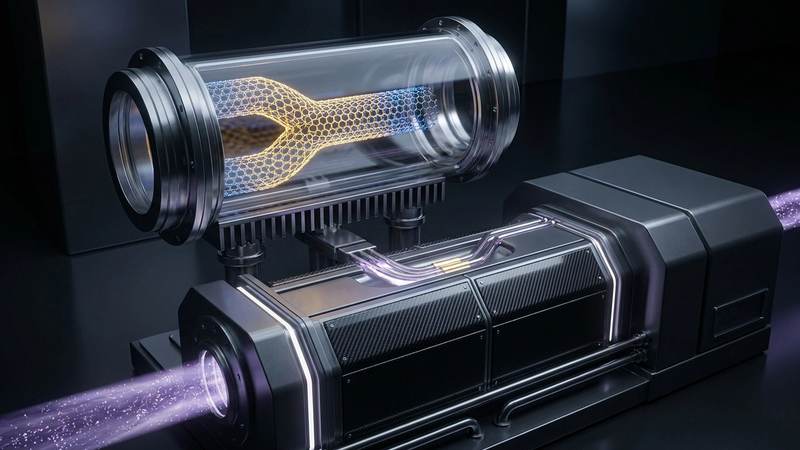
The Physics Behind Graphene Geometric Diodes
Graphene Geometric Diodes operate on a fascinating set of physical principles that leverage the material's unique electronic transport properties and the precise engineering of its physical shape. Unlike conventional p-n junction diodes, which rely on doping and bandgap differences to create rectification, geometric diodes achieve this by introducing an asymmetry in the device's physical layout. When a high-frequency AC field, such as a THz wave, is applied, this geometric asymmetry creates a preferential direction for charge carrier flow, resulting in a net DC current—the essence of rectification.
At the heart of their operation is the "hot electron" effect combined with thermoelectric phenomena. When THz radiation interacts with graphene, it excites the charge carriers (electrons and holes), raising their average energy and temperature significantly above the lattice temperature. These energetic carriers are known as "hot electrons." In a geometrically asymmetric structure, such as a bow-tie or a V-shaped antenna coupled to a narrow constriction, the hot electrons generated by the THz field experience different scattering and cooling rates depending on their direction of travel. This directional difference in energy relaxation creates an asymmetric potential profile.
Specifically, electrons moving towards the wider part of the geometric structure experience less scattering and can dissipate their energy more slowly, while those moving into a narrow constriction or sharp corner encounter higher scattering rates and cool down more rapidly. This spatial variation in electron temperature and energy relaxation leads to a thermoelectric voltage, known as the photothermoelectric effect, which drives a net current in a specific direction. The geometric design essentially acts as an "electron funnel," steering the hot carriers in a preferred direction and converting the oscillating THz energy into a measurable DC signal.
Furthermore, the interaction of incident THz radiation with graphene's intrinsic plasmons plays a crucial role in enhancing the rectification efficiency. Graphene plasmons can be excited by the THz field, resonating within the geometric structure and localizing the electromagnetic energy into subwavelength regions. This plasmonic resonance leads to a significant enhancement of the local electric field, which in turn amplifies the generation of hot electrons and strengthens the thermoelectric effect. The antenna structures typically integrated with these diodes are designed to efficiently couple free-space THz waves into these localized plasmonic modes, maximizing the device's responsivity.
The unprecedented operating frequency of 28 THz demonstrated by these diodes is a direct consequence of graphene's ultra-high carrier mobility and the extremely fast energy relaxation times of its hot electrons. The ability of charge carriers to respond and redistribute almost instantaneously to changes in the electric field, coupled with the rapid generation and flow of hot electrons, allows for rectification at frequencies far beyond the reach of conventional semiconductors. This fundamental understanding of hot electron dynamics, plasmonic enhancement, and geometric asymmetry is what underpins the revolutionary performance of graphene geometric diodes in the terahertz regime.
Manufacturing and Design Innovations
The creation of high-performance Graphene Geometric Diodes involves sophisticated manufacturing techniques and meticulous design considerations, blending advanced materials science with precision engineering. The foundation of these devices is high-quality graphene, typically produced through Chemical Vapor Deposition (CVD) methods. CVD allows for the growth of large-area, uniform graphene films on metallic substrates like copper, which can then be transferred onto various insulating substrates such as silicon dioxide (SiO2), silicon carbide (SiC), or flexible polymers. This transfer process is critical for integrating graphene into device architectures.
Once the graphene layer is established on a suitable substrate, advanced lithography techniques are employed to define the intricate geometric shapes that characterize these diodes. Electron-beam lithography (e-beam lithography) is often used for its superior resolution, enabling the patterning of nanoscale features down to tens of nanometers. This precision is essential for creating the sharp corners, narrow constrictions, and asymmetric designs that are critical for efficient THz rectification. Photolithography can also be used for larger features or in hybrid approaches, balancing resolution with throughput for scalability.
The device architecture typically includes an antenna structure integrated directly with the graphene rectifier. These antennas are designed to efficiently capture incident THz radiation and funnel it into the active graphene region. Common antenna designs include bow-tie antennas, dipole antennas, or V-shaped antennas, all optimized for specific THz frequencies. The antenna material, usually a highly conductive metal like gold, is deposited onto the graphene and substrate using evaporation or sputtering techniques, followed by lift-off processes to define the precise antenna geometry.
Optimizing the geometric shape of the graphene element is paramount for maximizing diode performance. Researchers continually explore various designs, from simple asymmetric constrictions to more complex multi-electrode structures, each aiming to enhance the hot electron flow and thermoelectric generation. The dimensions of these features—the width of the narrowest point, the angle of the V-shape, or the length of the antenna arms—are carefully engineered to resonate with specific THz frequencies and to maximize the rectification efficiency. Substrate choice also plays a role, influencing thermal management, optical coupling, and integration with other electronic components.
Further innovations in design include the integration of electrostatic gates. These gates allow for dynamic tuning of the graphene's carrier density, which in turn modulates its plasmonic response and hot electron dynamics. By applying a voltage to a gate electrode, the performance characteristics of the diode, such as its responsivity or operating frequency, can be actively controlled. This tunability opens avenues for reconfigurable THz systems. The ultimate goal is to integrate these individual diodes into large arrays for imaging applications or into complex on-chip systems for advanced signal processing, pushing the boundaries of miniaturization and functionality.
Applications: Transforming Industries with THz Technology
The advent of highly efficient Graphene Geometric Diodes operating in the terahertz regime promises to revolutionize numerous industries, unlocking applications that were previously impractical or impossible due to technological limitations. The ability to generate and detect THz waves with such high speeds and sensitivity opens up a vast spectrum of possibilities, from ultra-fast communication to advanced imaging and sensing.
One of the most immediate and impactful applications lies in ultrafast communication. As wireless data demands continue to surge, pushing beyond the limits of current 5G networks, THz frequencies offer an enormous untapped bandwidth for future generations of wireless communication, including 6G and beyond. Graphene geometric diodes can serve as critical components in THz transceivers, enabling incredibly high data rates for short-range, line-of-sight communication links. This could facilitate ultra-fast data transfer within data centers, between devices, or for specialized high-bandwidth satellite communication systems, reducing latency and increasing throughput dramatically.
In the realm of advanced imaging, THz technology offers unique advantages due to its non-ionizing nature and its ability to penetrate a wide range of non-metallic materials. Graphene geometric diodes are ideal for building compact, highly sensitive THz cameras and scanners. This technology can transform security screening, allowing for the detection of concealed weapons, explosives, or illicit drugs with high resolution and without harmful radiation exposure. In medical diagnostics, THz imaging could provide early detection of skin cancers, dental problems, or characterize tissue properties without invasive procedures. Industrial quality control would also benefit, enabling non-destructive inspection of plastics, ceramics, and composites for defects or impurities.
Spectroscopy is another area poised for significant transformation. Many molecules, particularly biological ones, have unique spectral fingerprints in the THz range corresponding to their vibrational and rotational modes. Graphene geometric diodes can be integrated into highly sensitive THz spectrometers for rapid and accurate chemical and biological sensing. This capability is invaluable for pharmaceutical quality control, environmental monitoring (detecting pollutants), food safety inspection, and even astronomical observation of molecular clouds. The compact size and high sensitivity of graphene-based detectors make them suitable for portable and field-deployable spectroscopy systems.
Beyond these established fields, graphene geometric diodes hold promise for future computing and quantum information technologies. Terahertz clock rates could lead to a new generation of ultra-fast processors, enabling computations at speeds currently unimaginable. The ability to manipulate and detect THz waves could also be crucial for developing novel memory architectures or for controlling quantum states in future quantum computers. The sheer speed and efficiency of these devices could fundamentally alter how data is processed and stored at the most fundamental levels of computing.
The Road Ahead: Challenges and Future Prospects
While Graphene Geometric Diodes have demonstrated groundbreaking performance at astonishing THz frequencies, several challenges must be addressed to transition this promising technology from laboratory breakthroughs to widespread commercial adoption. Overcoming these hurdles will pave the way for a new era of terahertz electronics and photonics, realizing the full potential of graphene.
One significant challenge lies in the scalability and uniformity of graphene production. While Chemical Vapor Deposition (CVD) has enabled large-area graphene growth, achieving wafer-scale production with consistent, high-quality material—free from defects and impurities—remains an active area of research. Reproducible transfer processes that preserve graphene's intrinsic properties are also critical. For mass manufacturing of THz devices, the ability to reliably produce millions of identical diodes with precise geometric features across large wafers is essential, requiring advanced fabrication infrastructure.
Another key area is the seamless integration of graphene geometric diodes with existing semiconductor platforms and packaging technologies. Current electronic systems are built around silicon and other III-V semiconductors. Developing robust and cost-effective methods to integrate graphene-based THz components with conventional microelectronics is vital for creating hybrid systems that leverage the strengths of both material classes. This includes considerations for signal routing, thermal management, and robust encapsulation to ensure long-term device reliability and performance in real-world environments.
Further improvements in device performance, particularly in terms of output power and noise reduction, are also ongoing research priorities. While the rectifying speeds are impressive, increasing the power handling capabilities for certain applications (e.g., THz sources) and simultaneously minimizing noise equivalent power for highly sensitive detection systems will broaden their utility. Researchers are exploring novel antenna designs, optimized graphene geometries, and heterostructures incorporating other 2D materials to enhance responsivity and signal-to-noise ratios.
The development of dynamically tunable and reconfigurable THz systems is another exciting prospect. While current devices offer some tunability via electrostatic gates, achieving broadband tunability or precise frequency selection across a wide THz range remains a goal. This would allow for adaptive THz systems that can adjust their operating parameters in real-time, offering greater flexibility for diverse applications such as multi-spectral imaging or agile communication systems. Research into novel gating schemes and hybrid material approaches is actively pursuing this advanced functionality.
Looking ahead, the future of graphene geometric diodes is incredibly bright. The continued refinement of fabrication techniques, coupled with a deeper understanding of the underlying physics, will lead to even more compact, energy-efficient, and higher-performing THz devices. We can anticipate the emergence of pervasive THz technology, integrated into everyday devices, transforming our ability to communicate, image, and sense the world around us. This technology is not just an incremental step but a fundamental leap towards unlocking the full potential of the terahertz spectrum, with graphene at its very core.
FAQ
1. What is the "terahertz gap"?
The "terahertz gap" refers to the challenging region of the electromagnetic spectrum between microwave and infrared frequencies, roughly 0.1 THz to 10 THz. Historically, it has been difficult to develop efficient, compact, and cost-effective electronic and photonic devices to generate, detect, and manipulate signals in this range, limiting its technological exploitation.
2. How do graphene geometric diodes differ from conventional diodes?
Conventional diodes, like p-n junction diodes, rely on doping and differences in semiconductor bandgaps to create a rectifying junction. Graphene geometric diodes, by contrast, are typically undoped and achieve rectification through physical asymmetry in their graphene structure. This asymmetry creates a preferential flow for "hot electrons" generated by THz radiation, converting AC signals into DC current without requiring a bandgap.
3. What makes graphene ideal for terahertz applications?
Graphene's exceptional properties make it ideal for THz applications, including its ultra-high carrier mobility, which allows electrons to move very fast with minimal scattering. It also has frequency-independent absorption across a broad spectrum, a linear electronic band structure, and supports highly confined and tunable plasmons. These attributes enable high-speed operation, efficient THz interaction, and sensitive detection.
4. What are the primary applications for this technology?
Graphene geometric diodes are poised to revolutionize several fields. Key applications include ultra-fast wireless communication (beyond 5G/6G), advanced non-ionizing imaging (security screening, medical diagnostics, industrial inspection), high-sensitivity spectroscopy (chemical and biological sensing, environmental monitoring), and potentially future high-speed computing and quantum information technologies.
5. What challenges remain for widespread adoption?
Despite their promise, challenges for widespread adoption include scaling up the production of high-quality, uniform graphene on large wafers and ensuring precise, reproducible nanoscale patterning. Seamless integration with existing semiconductor platforms and packaging is also crucial. Further improvements in output power, noise reduction, and developing dynamically tunable THz systems are active areas of research to enhance their practical utility.
Conclusion
The emergence of Graphene Geometric Diodes marks a pivotal moment in the advancement of terahertz technology, pushing the boundaries of what is possible in high-frequency electronics and photonics. By harnessing the unique quantum mechanical and electronic properties of graphene, these innovative devices have shattered previous speed records, demonstrating efficient rectification at an extraordinary 28 THz. This achievement is not merely an incremental gain but a fundamental redefinition of the operational limits for solid-state devices in the challenging terahertz spectrum.
The unparalleled carrier mobility, broad spectral absorption, and exceptional plasmonic properties of graphene provide the foundational advantages that allow these geometric diodes to bridge the long-standing terahertz gap. Through meticulous design, leveraging geometric asymmetry and hot electron dynamics, researchers have engineered devices capable of converting high-frequency electromagnetic waves into usable electrical signals with unprecedented efficiency. This scientific and engineering triumph opens vast new territories for technological exploration and application development.
As research progresses, addressing challenges related to scalability, integration, and performance optimization, the transformative potential of graphene geometric diodes will undoubtedly reshape numerous industries. From enabling ultra-fast, high-bandwidth communication networks to revolutionizing medical diagnostics, security screening, and chemical sensing, these diodes are set to become indispensable components in the next generation of technological systems. Graphene continues to assert its role as a cornerstone material for the future, and its geometric diodes stand as a testament to its extraordinary power to innovate and inspire.
Evaluate Our Quality
Serious about B2B integration? Test our premium Pulsed Electrical Resistive Carbon Heating turbostratic graphene in your lab. 100g sample packs available now.