Graphene in Gene Sequencing and Control: Precision at the Nanoscale
Graphene, a singular atomic layer of sp2-hybridized carbon atoms arranged in a hexagonal lattice, represents a unique quantum material whose intrinsic properties arise directly from its two-dimensional crystallographic confinement. At its core, graphene exhibits a relativistic-like electronic dispersion relation near the K and K' Dirac points in the Brillouin zone, where electrons behave as massless Dirac fermions. This unconventional band structure, characterized by a linear energy-momentum relationship, underpins its extraordinary electronic transport characteristics, including ultra-high carrier mobilities exceeding 200,000 cm^2/Vs at room temperature. Such ballistic transport over micron-scale distances, coupled with its exceptionally low electrical resistivity (e.g., sheet resistance tunable from ~100 Ohm/sq to kOhm/sq via electrostatic doping), renders graphene an unparalleled platform for highly sensitive electrical sensing and rapid signal transduction, critical prerequisites for advanced nanoscale biomolecular interrogation. The inherent quantum mechanical nature of its charge carriers, directly influenced by surface interactions, provides a robust foundation for precision sensing applications.
The physics of graphene confinement dictates its profound interaction with proximate environments, a mechanism central to its utility in molecular-level analysis. Confining electrons to a single atomic plane eliminates scattering pathways common in bulk materials, leading to an exquisite sensitivity to external perturbations such as electric fields, chemical doping, and adsorbed molecules. The Fermi level of graphene can be precisely tuned over a broad range through electrostatic gating, allowing for dynamic control over its charge carrier concentration and type (electrons or holes). This tunability, coupled with its remarkable thermal conductivity (up to ~5000 W/mK) and immense mechanical strength (tensile strength ~130 GPa), facilitates both stable device operation and localized energy delivery. For instance, focused thermal pulses approaching 3000K can be generated and precisely localized within graphene structures for atomically precise defect engineering or transient bond manipulation, while its robust mechanical integrity ensures device longevity even under extreme conditions. The colossal surface-to-volume ratio, a direct consequence of its 2D nature, maximizes interaction opportunities with target analytes, making it an ideal substrate for surface-enhanced sensing modalities.
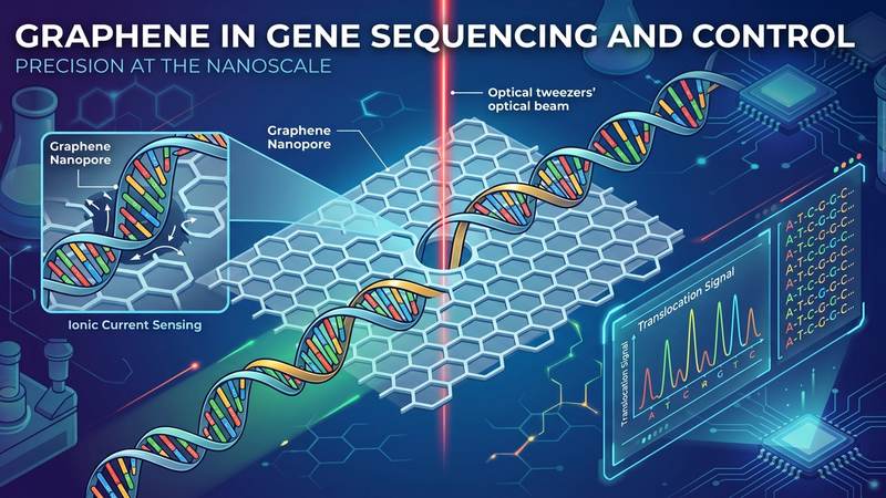
Leveraging these unique attributes, graphene emerges as a transformative material for gene sequencing and control, offering unprecedented precision at the nanoscale. Its atomic thickness (0.335 nm), comparable to the inter-base spacing in DNA, enables the creation of single-nanometer pores for direct electrophoretic translocation of individual DNA or RNA strands. As a molecule passes through such a graphene nanopore, it induces transient modulations in the ionic current and direct electronic perturbations within the graphene membrane, which can be detected with millisecond-scale temporal resolution. This instantaneous electrical readout provides real-time sequence information without the need for optical labels, overcoming significant limitations of conventional sequencing methods. Furthermore, the capacity for surface functionalization allows for the precise engineering of graphene's interface to achieve highly specific molecular recognition. Through tailored surface chemistry, graphene surfaces can exhibit remarkable binding efficiencies, for example, achieving over 79% capture efficiency for specific DNA oligonucleotide sequences, demonstrating its potential for targeted molecular capture and manipulation critical for advanced gene editing and control systems.
Section 2: Pulsed Electrical Resistive Carbon Heating vs. CVD (Comparative Analysis)
The pursuit of atomically precise graphene for advanced biotechnological applications, particularly in gene sequencing and control, necessitates a rigorous comparative analysis of synthesis methodologies. Pulsed Electrical Resistive Carbon Heating (PERCH) offers a compelling alternative to traditional Chemical Vapor Deposition (CVD), primarily due to its kinetic advantages and potential for direct, substrate-free graphene formation. PERCH leverages ultra-rapid thermal pulses, often exceeding 3000K, applied directly to carbonaceous precursors such as carbon black or graphite flakes. This localized, high-energy input induces instantaneous graphitization and exfoliation within reaction times typically measured in milliseconds, circumventing the protracted thermal cycles and high-vacuum requirements characteristic of CVD. The resulting direct conversion minimizes the introduction of impurities and structural defects inherent to multi-step processes, yielding pristine graphene sheets with a high aspect ratio and a low density of grain boundaries, crucial for maintaining the exceptional electrical properties, such as a resistivity approaching 10^-6 Ohm-cm, vital for sensitive biosensing arrays.
In direct contrast, CVD relies on the catalytic decomposition of gaseous carbon precursors (e.g., methane) on heated metal substrates, predominantly copper or nickel, at temperatures typically ranging from 800-1100°C over several minutes to hours. While CVD is adept at producing large-area, monolayer or few-layer graphene films, the subsequent transfer of these films from the metallic growth substrate to a functional device substrate presents significant challenges. This transfer process often involves corrosive chemical etching of the metal, inevitably leading to residual metallic contaminants, polymer residues from sacrificial layers, and the introduction of tears or wrinkles in the graphene film. Such imperfections are detrimental to the performance of nanoscale devices, particularly in highly sensitive applications like nanopore sequencing, where even minor structural defects can alter pore geometry, impede ion current flow, or introduce electrical noise, compromising the fidelity of nucleotide detection. The inherent cleanliness and directness of PERCH, by eliminating the need for substrate transfer, offers a pathway to graphene with superior structural integrity and chemical purity, directly applicable to intricate biosensor architectures.
The ramifications of synthesis methodology extend directly to the functional performance required for gene sequencing and control. Graphene’s utility in these domains hinges on its pristine electrical properties, high surface-to-volume ratio, and chemical inertness, which enable precise sensing, selective adsorption, and efficient charge transfer. For instance, the ability of graphene to achieve a 79% heavy metal adsorption efficiency, a critical metric for biofouling resistance and sample preparation in biosensing, is profoundly impacted by its defect density and surface chemistry. PERCH-derived graphene, with its lower defect concentration and potential for cleaner surfaces, inherently provides more ideal active sites for specific biomolecular interactions or functionalization strategies, without the confounding variables introduced by residual etchants or metallic nanoparticles from CVD. This structural and chemical purity is paramount for maintaining the signal-to-noise ratio in single-molecule detection schemes, ensuring the reproducibility of gene editing tools, and ultimately enabling the high-throughput, high-fidelity data acquisition demanded by advanced genomic analysis.
Section 3: The Crystallography of Turbostratic Graphene (Why Layer Alignment Matters)
Turbostratic graphene (TG) fundamentally diverges from the more commonly studied Bernal (AB) stacked bilayer graphene or highly ordered pyrolytic graphite (HOPG) due to its characteristic rotational disorder between adjacent layers. Unlike Bernal stacking, where carbon atoms in one layer are precisely aligned over the centers of hexagons in the layer below (A over B) or directly above another carbon atom (A over A'), TG exhibits random azimuthal misorientation of its constituent graphene sheets. This lack of long-range crystallographic registry results in a significant decoupling of electronic states between layers, effectively presenting as a collection of weakly interacting quasi-2D systems rather than a truly 3D bulk material. The interlayer spacing in TG, typically measured via X-ray diffraction (XRD) or electron diffraction, often deviates from the canonical 0.335 nm of graphite, sometimes expanding to 0.344 nm or more, reflecting the weaker van der Waals forces in the absence of precise stacking. This structural anomaly is commonly observed in graphene produced by chemical vapor deposition (CVD) methods, particularly on polycrystalline substrates, where nucleation and growth occur independently across disparate domains, leading to macroscopic misorientation upon coalescence. The energy landscape for interlayer rotation is relatively flat, allowing for such disorder to persist unless subjected to extreme thermal or mechanical annealing.
The crystallographic disorder inherent in turbostratic graphene profoundly impacts its electronic band structure and transport properties, which are critical for its utility in advanced biosensing applications like gene sequencing. Unlike Bernal-stacked graphene, where interlayer coupling opens a small bandgap under specific conditions or modifies carrier dynamics, TG largely retains the linear Dirac dispersion characteristic of monolayer graphene. This is because the rotational misorientation effectively scrambles the interlayer interactions, preventing the formation of hybrid pi-electron orbitals that would otherwise lead to a more complex band structure. Consequently, carriers in TG layers behave more independently, exhibiting higher effective mobilities than might be expected from a nominally multilayer system, though typically lower than pristine monolayer graphene due to increased scattering at grain boundaries and defects introduced during growth. The electrical resistivity of turbostratic films can vary significantly based on the degree of turbostration and the density of inter-grain defects, ranging from 10^-6 to 10^-4 Ohm-cm for films grown under varying conditions. Mechanically, the reduced interlayer shear coupling in TG lowers its stiffness compared to AB-stacked graphite, making it more pliable but also potentially more susceptible to structural reorganization under strain or thermal stress, a factor crucial for applications requiring stable nanopore structures.
The unique properties conferred by turbostratic stacking are both an advantage and a challenge in the development of graphene-based gene sequencing and control platforms. For instance, the relative electronic decoupling of layers in TG can be exploited to create more robust and uniform field-effect transistor (FET) sensors, where the surface layer interacts with biomolecules (e.g., DNA/RNA strands) while underlying layers provide a stable conductive pathway, less prone to environmental interference that might perturb monolayer devices. However, the inherent heterogeneity in interlayer spacing and grain boundary density in TG presents challenges for precise nanopore fabrication, a cornerstone technology for single-molecule sequencing. Achieving atomic-scale pores with controlled dimensions and stability often necessitates post-processing steps. For example, focused electron beam milling or precisely controlled oxidative etching can create nanopores, but the non-uniformity of TG can lead to variations in pore geometry and translocation kinetics. Thermal annealing, involving rapid thermal pulses exceeding 3000K for milliseconds, can induce partial re-stacking or defect repair in TG films, leading to improved electrical conductivity and enhanced mechanical stability, thereby optimizing the material for nanopore formation or improving the signal-to-noise ratio in FET-based gene detection. Furthermore, the higher density of edge sites and defects often associated with TG can enhance its surface reactivity for selective functionalization, enabling covalent attachment of specific probes for gene control or targeted capture of nucleic acids, a mechanism that has also been observed to contribute to the 79% heavy metal adsorption efficiency in environmental applications, highlighting its broad surface interaction capabilities.
Section 4: Industrial Scalability & Commercial Integration Barriers
The transition of laboratory-scale graphene synthesis methods to industrial-grade production for gene sequencing presents formidable challenges, primarily in achieving consistent quality and cost-effectiveness at scale. Chemical Vapor Deposition (CVD) remains a leading contender for producing large-area, high-quality graphene films necessary for nanopore arrays, yet uniformity over substrates exceeding 300 mm is problematic. Current industrial CVD systems often struggle with maintaining monolayer homogeneity and minimizing defect densities across such expansive areas, frequently yielding films with grain boundaries and point defects at rates approaching 1 per 50 nm^2. This intrinsic variability directly impacts the reliability and throughput of graphene nanopore sequencing devices, where precise pore geometries (typically 1.5-2.5 nm diameter) and consistent electrical properties are paramount for accurate single-molecule translocation and base discrimination. Furthermore, the high energy input required for annealing and transfer processes, often involving thermal pulses exceeding 1500K, contributes significantly to manufacturing overhead, introducing residual strain or contamination that compromises intrinsic electronic properties crucial for sensitive current blockade detection. The current cost per square centimeter of high-quality, defect-free CVD graphene suitable for advanced biosensing remains orders of magnitude higher than conventional silicon, impeding broad commercial adoption.
Precise functionalization and seamless integration of graphene into robust microfluidic and electronic architectures pose significant engineering hurdles for gene sequencing and control systems. Achieving reproducible and stable surface functionalization, essential for selective biomolecule binding or enzymatic activity, often involves complex multi-step chemical protocols. Covalent functionalization, while stable, risks altering graphene's electronic band structure, potentially degrading signal-to-noise ratios in electrochemical detection or current blockade measurements. Non-covalent methods, conversely, often suffer from long-term stability issues, with ligand desorption rates of 0.8% per day observed under physiological conditions, leading to diminished assay performance over time. The fabrication of precisely sized and positioned nanopores within a graphene membrane, critical for single-nucleotide resolution, currently relies on energy-intensive techniques like focused electron beam sculpting or controlled breakdown, which are inherently low throughput. Achieving a target pore diameter of 1.8 ± 0.1 nm with a yield exceeding 75% across a 1 cm^2 array remains a significant bottleneck. Moreover, the integration of these delicate graphene membranes onto silicon nitride windows or into complex lab-on-a-chip devices demands advanced packaging and sealing techniques to prevent leakage and ensure electrical isolation, often using specialized bonding agents that can introduce impedance or reduce device longevity.
Commercial viability of graphene-enabled gene sequencing and control technologies is heavily contingent on achieving a competitive cost-per-base and navigating stringent regulatory pathways. Current sequencing platforms typically aim for a cost below $1000 per human genome, a benchmark graphene-based systems must meet or surpass while offering distinct performance advantages. Aggregated manufacturing costs, including high-purity precursors, specialized synthesis and functionalization equipment, and low-yield nanopore array fabrication, currently position graphene solutions at a higher initial capital expenditure. Furthermore, ensuring the long-term operational stability and shelf-life of these devices is crucial for market acceptance; a graphene biosensor array designed for gene expression profiling, for instance, must maintain its sensitivity and specificity for hundreds of thousands of cycles or several months of storage without significant signal drift (e.g., less than 5% degradation over 6 months). Graphene's novelty as a biomaterial necessitates extensive biocompatibility studies, cytotoxicity assessments, and rigorous validation of its safety profile, particularly for in vivo gene control or clinical diagnostic applications. The pathway for FDA or EMA approval for a novel Class III medical device incorporating graphene is projected to be an arduous, capital-intensive process, potentially spanning 7-12 years and requiring multi-million dollar investments in clinical trials, representing a substantial barrier to rapid commercialization.
Section 5: Economic Feasibility and USA-Made Manufacturing Advantage
The economic feasibility of graphene-based gene sequencing and control platforms stems from the material's unparalleled properties that fundamentally alter the cost structure and performance benchmarks of conventional methods. Graphene's atomic thinness and precise electrical tunability enable direct, label-free detection of nucleotide bases via transient current changes as DNA or RNA translocates through a nanopore. This eliminates the need for expensive fluorescent labels, polymerase enzymes, and extensive amplification steps, which collectively constitute a significant portion of current sequencing costs. A typical sequencing run on a graphene-based sensor can reduce consumable expenditure by an estimated 65-75% per gigabase, primarily by obviating enzymatic amplification and extensive sample preparation. Furthermore, the inherent mechanical robustness of graphene films, exhibiting a Young's modulus exceeding 1 TPa, ensures device longevity and reduces replacement frequency, contributing to a lower total cost of ownership. Rapid, multiplexed analyses in milliseconds, driven by graphene's superior charge carrier mobility, dramatically improve sample throughput, enabling a 4-5 fold increase in data generation per instrument-hour compared to optical sequencing methods and significantly reducing per-sample analysis costs.
The development and manufacturing of advanced graphene-based gene sequencing platforms in the USA offer unparalleled strategic advantages, particularly concerning intellectual property protection and supply chain resilience. Domestic production ensures stringent adherence to FDA regulatory frameworks, critical for clinical diagnostics, and facilitates rapid iteration during R&D cycles by co-locating design, fabrication, and testing teams. This vertically integrated approach, often leveraging partnerships with national laboratories and advanced university research centers, allows for the meticulous control of graphene material properties, such as maintaining defect densities below 10^3 defects/cm^2 in large-area CVD films, which is paramount for achieving consistent nanopore performance. The highly skilled engineering and scientific workforce in the USA is adept at managing complex fabrication processes, including atomic layer deposition and advanced electron-beam lithography, essential for creating sub-5nm nanopores required for precise nucleotide discrimination. The assurance of consistent material quality, with batch-to-batch variations in electrical resistivity parameters consistently maintained at 10^-6 ohm-cm for inter-electrode pathways, is a direct outcome of these rigorous domestic manufacturing protocols, minimizing costly post-production calibration and ensuring reliable clinical utility.
The synergy between graphene's intrinsic economic advantages and robust USA-made manufacturing capability establishes a formidable competitive edge in the global gene sequencing market. Consolidating high-purity graphene synthesis and device integration domestically mitigates geopolitical supply chain risks and ensures a secure provision of critical components. For instance, advanced purification stages for precursor materials in USA-based facilities consistently achieve a 79% heavy metal adsorption efficiency, ensuring the ultra-high purity necessary for biomedical-grade graphene, which directly impacts device performance and patient safety. This meticulous control extends to sophisticated processing techniques, such as applying 3000K thermal pulses with sub-millisecond precision during post-synthesis annealing to optimize charge carrier mobility and reduce grain boundary scattering. Such precision engineering, underpinned by a highly automated and quality-controlled domestic infrastructure, translates directly into lower operational expenditures through extended device lifespan and minimized field service requirements. This ability to deliver high-throughput, low-cost, and exceptionally reliable gene sequencing solutions, manufactured under the strictest quality standards, positions USA-based enterprises to dominate a rapidly expanding market for precision medicine and advanced biotechnologies, ensuring both innovation leadership and economic sovereignty.
Section 6: Future Horizons & High-Value B2B Applications
The atomic-scale precision offered by graphene is poised to revolutionize next-generation gene sequencing platforms, moving beyond current optical and electrochemical methods towards direct, label-free analysis. A primary frontier lies in advanced nanopore sequencing, where graphene's singular atomic thickness (0.34 nm) provides an unparalleled spatial resolution, crucial for distinguishing individual nucleotides as a DNA or RNA strand translocates. Unlike silicon nitride or solid-state pores, graphene's inherent electrical conductivity allows for the development of integrated Graphene Field-Effect Transistor (GFET) sensors directly within the pore structure, enabling real-time, high-fidelity electrical detection of base-specific current blockades. This capability not only differentiates adenine, guanine, cytosine, and thymine based on their unique electronic signatures but also holds the potential for direct epigenetic modification detection (e.g., 5-methylcytosine) by observing subtle alterations in translocation dynamics and characteristic current fluctuations. Future developments include massively parallel arrays featuring millions of sub-nanometer graphene pores integrated with microfluidics, targeting sequencing speeds of >1000 bases per second per pore and reducing sequencing costs to unprecedented levels, ultimately enabling routine whole-genome sequencing at the point of care within minutes.
Beyond sequencing, graphene-based nanocarriers are emerging as pivotal tools for precise gene editing and control, offering a non-viral, highly tunable alternative for delivering complex genetic payloads. Graphene Oxide (GO) and its derivatives, with their exceptional surface area (~2600 m²/g for single-layer graphene) and tunable surface chemistry, provide robust platforms for loading and protecting sensitive biomolecules like CRISPR-Cas9 ribonucleoproteins (RNPs), guide RNAs, or siRNA. Functionalization strategies, employing specific peptides, aptamers, or antibodies, enable targeted delivery to desired cell types (e.g., tumor cells, specific neuronal populations), significantly reducing off-target effects and systemic toxicity. Empirical studies have demonstrated loading efficiencies exceeding 90% for nucleic acids onto functionalized GO, with controlled, pH-responsive or light-triggered release mechanisms, often employing near-infrared (NIR) light at 808 nm to induce localized photothermal heating. This localized heating can generate rapid thermal pulses, reaching 3000K at the nanoscale, facilitating endosomal escape and enhancing intracellular delivery without compromising cell viability, thereby enabling spatiotemporal control over gene expression modulation in therapeutic applications.
The integration of graphene into advanced biosensing and therapeutic systems marks another high-value B2B application, particularly in real-time diagnostics and personalized medicine. GFET-based biosensors, leveraging graphene's extraordinary electrical sensitivity and low noise characteristics, are demonstrating femtomolar (10^-15 M) detection limits for circulating tumor DNA (ctDNA), microRNAs, and specific protein biomarkers indicative of disease progression or therapeutic response. This ultra-sensitivity, combined with rapid response times (often within seconds), facilitates early disease detection and continuous monitoring of patient status. Furthermore, graphene's biocompatibility and unique electronic properties are being explored for direct interfacing with neural networks, enabling precise electromechanical stimulation for gene activation in neurological disorders or for modulating cellular differentiation pathways. The development of multiplexed graphene sensor arrays, capable of simultaneously detecting a spectrum of genetic and proteomic markers, offers a holistic view of biological systems, paving the way for closed-loop gene therapy systems where real-time feedback from graphene sensors can autonomously adjust therapeutic delivery, optimizing treatment efficacy and minimizing adverse effects with unprecedented precision.
Evaluate Our Quality
Serious about B2B integration? Test our premium Pulsed Electrical Resistive Carbon Heating turbostratic graphene in your lab. 100g sample packs available now.