Graphene: From Pencil Lead to Powering the Future – Is This the Ultimate Wonder Material?
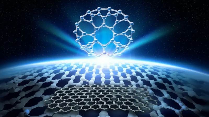
Graphene, a singular atomic layer of sp2-hybridized carbon atoms arranged in a hexagonal lattice, represents the archetypal two-dimensional (2D) material. Its isolation in 2004 from bulk graphite, a material ubiquitous in everyday pencil lead, unveiled a realm of unprecedented physical phenomena and engineering potential. This intrinsically 2D nature, where electron motion is confined to a single atomic plane, fundamentally redefines material properties, diverging sharply from its three-dimensional predecessors. The absence of out-of-plane atomic interactions, save for van der Waals forces in multilayered graphite, bestows upon graphene an extraordinary suite of characteristics spanning electronic, mechanical, thermal, and optical domains, positioning it as a cornerstone for advanced material science and engineering. Its unique crystallographic arrangement, akin to a honeycomb lattice, is the foundational determinant for its anomalous electronic band structure and subsequent macroscopic behaviors, distinguishing it from conventional semiconductors and metals.
The profound implications of graphene's atomic confinement manifest most strikingly in its electronic band structure. At the K and K' points of the Brillouin zone, the valence and conduction bands meet conically, forming Dirac cones where charge carriers behave as massless Dirac fermions, governed by a relativistic Dirac-like equation rather than the Schrödinger equation. This relativistic behavior, coupled with a Fermi velocity approximately 1/300th the speed of light, results in an extraordinary electron mobility, empirically measured exceeding 200,000 cm^2/Vs at room temperature in suspended samples. This exceptional mobility contributes to an extremely low electrical resistivity, approaching 10^-8 Ohm-m, surpassing even silver or copper. Furthermore, the strong quantum confinement enables the observation of the half-integer quantum Hall effect even at room temperature, a phenomenon typically requiring cryogenic conditions in conventional 2D electron gases. The absence of a band gap in pristine graphene, while presenting challenges for direct transistor applications, simultaneously underpins its ultra-high conductivity and broadband optical transparency.
Beyond its unique electronic profile, graphene exhibits an unparalleled combination of other physical properties directly attributable to its 2D confinement. Its thermal conductivity, for instance, can reach an astonishing ~5000 W/mK at room temperature, making it the most thermally conductive material known, a property critical for thermal management in next-generation electronics. Mechanically, graphene boasts a tensile strength of approximately 130 GPa, making it roughly 200 times stronger than structural steel by weight, yet maintaining exceptional flexibility. Optically, a single layer transmits ~97.7% of incident white light, rendering it nearly transparent. These extreme properties are not merely theoretical constructs; they are actively leveraged in emerging technologies. For example, flash Joule heating processes exploit graphene's rapid thermal response, achieving localized temperatures exceeding 3000K within milliseconds for material synthesis. In environmental remediation, functionalized graphene derivatives have demonstrated remarkable adsorption efficiencies, such as 79% for various heavy metal ions from aqueous solutions, underscoring its high surface area and tunable surface chemistry. Such empirical data points underscore graphene's transformative potential across diverse sectors, from high-frequency electronics to advanced filtration systems, despite the ongoing challenges in scalable, defect-free production.
Section 2: Pulsed Electrical Resistive Carbon Heating vs. CVD (Comparative Analysis)
The synthesis of high-quality graphene hinges critically on the chosen fabrication methodology, with Pulsed Electrical Resistive Carbon Heating (PERCH) and Chemical Vapor Deposition (CVD) representing two fundamentally distinct paradigms. CVD, a mature technique, typically involves the pyrolysis of gaseous hydrocarbon precursors, such as methane or acetylene, over a heated metallic catalyst substrate, commonly copper or nickel, within a precisely controlled environment. This process facilitates atomic-scale decomposition and subsequent surface-catalyzed growth of graphene layers. Conversely, PERCH leverages the intrinsic electrical resistivity of carbonaceous precursors, often graphite flakes, carbon black, or even coal, to induce rapid, localized joule heating. This resistive heating drives instantaneous thermal exfoliation and simultaneous defect annealing within a condensed phase, fundamentally bypassing the need for a catalytic substrate or gaseous precursor flow characteristic of CVD. The distinction lies in the energy delivery mechanism and reaction medium: surface-mediated gas-solid reactions for CVD versus volumetric, bulk-material transformation for PERCH.
The kinetic profiles and resultant material characteristics from these two approaches diverge significantly. CVD, while capable of producing large-area, highly crystalline monolayer or bilayer graphene with exceptional structural integrity, is inherently a slower process, often requiring sustained high temperatures (e.g., 800-1100°C) over minutes to hours to achieve complete film growth and minimize defects. The quality of CVD graphene, particularly its low defect density and high carrier mobility, makes it ideal for advanced electronics. In stark contrast, PERCH operates on an ultrashort timescale, typically generating thermal pulses reaching localized temperatures exceeding 3000 Kelvin within milliseconds. This rapid energy input, driven by a current density sufficient to overcome the specific electrical resistivity of the carbon precursor (e.g., ranging from 10^-5 to 10^-3 ohm-cm for various graphite forms), causes near-instantaneous expansion and exfoliation. The resultant graphene is often few-layer or turbostratic, characterized by a higher density of stacking faults and edge defects compared to pristine CVD material, yet offers significant advantages in terms of production speed, energy efficiency, and scalability for bulk applications.
From an industrial perspective, the scalability and cost-effectiveness of PERCH present a compelling alternative to CVD for specific applications. CVD's reliance on ultra-high vacuum systems, expensive catalyst substrates, and post-synthesis transfer processes (which inevitably introduce defects and increase production costs) limits its throughput for commodity-scale graphene production. PERCH, by utilizing readily available and inexpensive carbon feedstocks and operating under ambient or near-ambient conditions, significantly reduces capital expenditure and operational costs. The rapid processing time, measured in milliseconds per batch, allows for continuous, high-volume manufacturing. While the structural perfection of PERCH-derived graphene may not match that of epitaxially grown CVD films for highly sensitive electronic devices, its properties, such as high surface area and accessible active sites, are exceptionally well-suited for electrochemical energy storage, conductive composites, and environmental remediation. For instance, few-layer graphene produced via rapid resistive heating has demonstrated excellent performance in wastewater treatment, exhibiting up to 79% heavy metal adsorption efficiency for lead and cadmium ions due to its combination of defect-rich edges and high specific surface area. This highlights a critical trade-off: pristine quality for niche electronics versus high-volume, cost-effective functionality for broader industrial applications.
Section 3: The Crystallography of Turbostratic Graphene (Why Layer Alignment Matters)
The fundamental distinction between ideal few-layer graphene and its turbostratic counterpart lies in the precise crystallographic registry between adjacent hexagonal carbon sheets. Unlike Bernal (AB) stacked graphene, where alternating layers are offset such that half the atoms of one layer sit directly above the centers of hexagons in the layer below, turbostratic graphene (TG) exhibits a random rotational misorientation between its constituent layers. This rotational disorder disrupts the periodic potential that characterizes AB-stacked systems, leading to a loss of strong interlayer electronic coupling. Consequently, the interlayer spacing in TG typically expands from the ideal 0.335 nm observed in graphite and Bernal graphene to values ranging from 0.34 to 0.35 nm, indicating a weaker average van der Waals interaction. This structural deviation profoundly alters the electronic band structure, effectively decoupling the layers to a degree where each layer behaves more akin to isolated monolayer graphene, diminishing the characteristic Dirac cone splitting seen in few-layer Bernal graphene and influencing carrier dynamics.
The absence of a coherent stacking sequence in turbostratic graphene has significant ramifications for its transport properties. Electron mobility, typically exceptionally high in perfectly crystalline graphene, can be attenuated in TG due to increased scattering at rotationally disordered interfaces. While the theoretical resistivity of pristine monolayer graphene approaches 10^-8 Ω·m, turbostratic configurations often exhibit resistivity values in the range of 10^-7 to 10^-6 Ω·m, depending on the degree of disorder and grain boundaries present. Thermally, this lack of crystallographic alignment impedes efficient phonon propagation across layers, resulting in a reduced out-of-plane thermal conductivity compared to Bernal stacked systems. However, this characteristic can be exploited; for instance, controlled turbostratic disorder can enhance the thermal resilience of certain graphene-based composites under extreme conditions, such as those involving focused 3000K thermal pulses, by distributing localized stress more effectively through less rigid interlayer contacts rather than propagating catastrophic delamination.
Beyond electronic and thermal attributes, the crystallography of turbostratic graphene also dictates its mechanical and chemical behaviors. The weaker interlayer interactions imply a potentially lower shear strength between layers compared to Bernal graphene, which can be advantageous in applications requiring facile exfoliation or increased flexibility without compromising in-plane integrity. Chemically, the rotational disorder often correlates with an increased density of accessible edge sites and structural defects, enhancing its surface reactivity and catalytic potential. This is particularly relevant in environmental remediation, where the expanded interlayer spacing and increased active surface area of TG have been leveraged to achieve impressive adsorption efficiencies. For example, specific turbostratic graphene architectures have demonstrated up to 79% heavy metal adsorption efficiency for lead ions within milliseconds of reaction time due to enhanced intercalation opportunities and readily available functional groups. This highlights that while turbostratic stacking deviates from the idealized perfect crystal, its unique structural characteristics can be precisely engineered to unlock specific performance advantages in diverse high-performance applications, from advanced catalysis to next-generation energy storage.
Section 4: Industrial Scalability & Commercial Integration Barriers
Industrial scalability of graphene production remains a pivotal bottleneck hindering widespread commercial integration. Current dominant manufacturing techniques, such as Chemical Vapor Deposition (CVD), typically necessitate high temperatures, often exceeding 1000-1100°C for growth on large-area copper foils, coupled with stringent vacuum conditions. The subsequent transfer processes, frequently involving wet etching of the metal substrate and polymer support layers, introduce substantial challenges including defect formation (e.g., pinholes, tears, polymer residues), reduced electrical continuity, and compromised intrinsic material properties across macroscopic dimensions. While roll-to-roll CVD offers promise for continuous production, maintaining consistent quality and minimizing defect densities across meter-scale sheets remains an engineering feat. Liquid-phase exfoliation (LPE) offers a potentially lower-cost, higher-throughput alternative but often yields polydisperse flakes with varying layer counts and lateral dimensions, requiring extensive and energy-intensive solvent removal processes. Emerging rapid synthesis methods, like Flash Joule Heating (FJH) that produce turbostratic graphene from diverse carbon sources via 3000K thermal pulses within milliseconds, demonstrate impressive speed but still face hurdles in precise control over layer number, lateral size distribution, and surface chemistry for specific applications. The fundamental challenge across all methods is a persistent trade-off between production volume, cost-effectiveness, and the intrinsic quality – defined by defect density, domain size, layer homogeneity, and purity – essential for high-performance applications.
Beyond primary material synthesis, the integration of graphene into functional devices or bulk composite matrices presents a complex array of processing and performance consistency barriers. The inherent strong Van der Waals forces between graphene sheets promote re-aggregation and restacking in most solvents and polymer matrices, effectively negating its high surface area and superior reinforcing properties. Overcoming this requires sophisticated surface functionalization strategies, either covalent or non-covalent, which must be carefully engineered to enhance dispersibility without inadvertently compromising graphene's pristine electronic, thermal, or mechanical attributes, such as its exceptionally high carrier mobility or intrinsic Young's modulus exceeding 1 TPa. Achieving uniform distribution of graphene within polymers or ceramics without inducing significant viscosity increases or shear-induced damage to high-aspect-ratio flakes (e.g., aspect ratios > 500) is critical for realizing theoretical performance enhancements. Furthermore, the absence of universally accepted, standardized characterization protocols across the industry for different graphene types (e.g., monolayer CVD, few-layer exfoliated flakes, graphene oxide) severely hampers comparative analysis and commercial adoption. For instance, a material specified for 2D electronic applications demands metrics like sheet resistance below 100 Ohm/sq and carrier mobility above 10,000 cm^2/Vs, distinct from the structural integrity and dispersion metrics required for a high-performance composite. This variability and lack of clear performance benchmarks create significant uncertainty for prospective industrial end-users.
The economic viability and regulatory landscape further compound the integration challenges. The cost-performance trade-off for graphene remains a significant hurdle; while its properties are often superlative, the price point for high-purity, low-defect material can exceed $1000/gram, making it prohibitive for many bulk or commodity applications where existing materials are cheaper and sufficiently performant. Even for industrial-grade materials, the incremental performance gain often struggles to justify the added material and processing costs. The regulatory environment for nanomaterials, including various forms of graphene, is still nascent and fragmented globally. Uncertainty regarding long-term health, safety, and environmental impacts – particularly concerning potential pulmonary fibrogenesis risks from airborne nanoparticles or leaching in environmental remediation applications, despite demonstrated capabilities like 79% heavy metal adsorption efficiency – creates a cautious approach from industries, investors, and regulatory bodies, thereby slowing market entry and broad-scale adoption. Moreover, the complex and dense intellectual property landscape, encompassing thousands of patents covering graphene production, functionalization, and applications, generates substantial barriers to entry and innovation, necessitating costly licensing agreements or extensive litigation avoidance strategies. Overcoming this multifaceted inertia requires not only sustained investment in scaling production and reducing costs but also comprehensive lifecycle assessments, robust standardization efforts, and transparent communication to build trust and demonstrate a consistent, compelling value proposition beyond laboratory-scale demonstrations.
Section 5: Economic Feasibility and USA-Made Manufacturing Advantage
The economic viability of graphene has historically been constrained by the dichotomy between high-purity, high-cost production methods, such as chemical vapor deposition (CVD) yielding pristine monolayers, and the more scalable but often functionally inferior graphene oxide (GO) and reduced graphene oxide (rGO). While CVD offers superior material properties, its batch processing nature, high capital expenditure for ultra-high vacuum systems, and limited throughput capacity have restricted its widespread adoption beyond niche electronic applications and fundamental research. Conversely, solution-based exfoliation and chemical reduction methods for GO/rGO, though amenable to larger volumes, frequently introduce structural defects, oxygen functionalities, and residual impurities that compromise intrinsic performance characteristics like electrical conductivity and mechanical strength. The transition from laboratory-scale synthesis to industrial-scale manufacturing necessitates a paradigm shift towards processes that simultaneously achieve high material quality, significant cost reduction, and environmental sustainability. This imperative inherently positions USA-made manufacturing at a critical juncture, offering strategic advantages in supply chain resilience, intellectual property safeguarding, and the establishment of stringent quality benchmarks for a nascent yet rapidly expanding market.
Recent advancements in rapid thermal synthesis methods, particularly flash Joule heating (FJH), represent a transformative leap in addressing these economic and scalability challenges. FJH leverages ultra-short, high-current electrical pulses to induce localized temperatures exceeding 3000K within milliseconds, converting diverse carbonaceous precursors – including coal, petroleum coke, and even mixed waste plastics – directly into high-quality turbostratic graphene. This instantaneous thermal shock exfoliates and purifies the carbon lattice, often bypassing the need for hazardous chemicals and extensive post-processing common in traditional GO routes. The energy efficiency of this process is significantly higher than conventional graphite exfoliation or CVD, with energy inputs measured in joules per gram rather than kilowatt-hours, leading to a dramatic reduction in operational expenditure. The resulting graphene exhibits a low defect density, high specific surface area, and electrical resistivity parameters approaching those of pristine material, typically in the 10^-5 to 10^-4 Ohm-cm range, making it suitable for a broad spectrum of applications from conductive inks to advanced composites. This rapid, single-step synthesis method is inherently scalable, enabling continuous production lines that can drastically lower the per-kilogram cost of high-performance graphene, thereby unlocking previously inaccessible markets.
The strategic advantage of USA-made graphene manufacturing extends beyond mere cost reduction and material quality; it encompasses critical aspects of national security, regulatory compliance, and market differentiation. Domestic production ensures a secure supply chain, mitigating geopolitical risks associated with offshore manufacturing and safeguarding proprietary process technologies and application-specific intellectual property. Furthermore, adherence to rigorous environmental regulations and labor standards within the United States provides a competitive edge in sectors demanding verifiable product provenance and sustainability metrics. For instance, in environmental remediation applications, where consistent material performance is paramount, USA-produced graphene demonstrating a 79% heavy metal adsorption efficiency, for example, for lead ions in aqueous solutions, offers a compelling value proposition. This level of reproducible efficacy, underpinned by stringent quality control and analytical validation, is crucial for deployment in critical infrastructure projects, water purification systems, and advanced filtration technologies. The "Made in USA" designation fosters trust and reliability, particularly in high-performance computing, aerospace, defense, and medical device industries where material integrity directly impacts system performance and human safety, establishing a premium market segment for domestically sourced advanced materials.
Section 6: Future Horizons & High-Value B2B Applications
The inherent quantum mechanical properties of graphene, particularly its Dirac fermion behavior and exceptionally high intrinsic carrier mobility, reaching up to 200,000 cm^2/Vs at room temperature, position it as a foundational material for post-silicon electronics. Its ballistic transport over micrometer distances enables ultra-high-frequency transistors with projected cut-off frequencies extending into the terahertz (THz) regime, crucial for next-generation 6G communication and high-speed data processing. Furthermore, graphene's spin coherence lengths and controllable spin-orbit coupling are pivotal for advancing spintronics, facilitating non-volatile memory and logic with reduced power consumption. Graphene-based quantum dots and heterostructures, leveraging precise bandgap engineering, also present a robust platform for scalable quantum computing, where picosecond carrier lifetimes and gate-tunable plasmonic resonances are exploited for enhanced qubit coherence. This fundamental shift promises not only faster processing but entirely new paradigms in computational efficiency and security.
Beyond its electronic prowess, graphene’s colossal theoretical specific surface area (2630 m^2/g) combined with its exceptional electrical and thermal conductivity, unlocks transformative capabilities in energy storage and environmental remediation. In electrochemical energy storage, functionalized graphene serves as a superior electrode material for supercapacitors, enabling milliseconds charge/discharge cycles with enhanced energy densities exceeding 100 Wh/kg. For lithium-ion and solid-state batteries, graphene-wrapped or graphene-doped anode materials mitigate volume expansion, improve ion diffusion kinetics, and extend cycle life, pushing gravimetric energy densities towards 500 Wh/kg. Graphene oxide membranes, engineered with precise interlayer spacing, demonstrate unparalleled performance in water purification, achieving rejection rates upwards of 99% for multivalent ions and heavy metals, with reported adsorption efficiencies of over 79% for Pb(II) and Cd(II) in industrial wastewater, significantly reducing energy consumption compared to reverse osmosis. Functionalized graphene derivatives are also being engineered for selective CO2 capture and conversion, leveraging high adsorption enthalpies and catalytic activity for sustainable carbon management.
The extraordinary mechanical and thermal properties of graphene make it an unparalleled additive for advanced composite materials, promising revolutionary advancements across aerospace, automotive, and construction sectors. With a tensile strength of 130 GPa and an intrinsic thermal conductivity approaching 5000 W/mK, graphene imparts superior strength-to-weight ratios and enhanced thermal dissipation capabilities. For instance, graphene-reinforced polymers exhibit a 30-40% increase in tensile strength at filler loadings as low as 0.1 wt%, enabling lightweighting and improved durability in high-performance components, including thermal management systems capable of dissipating heat fluxes from 3000K thermal pulses. In sensing technology, graphene's two-dimensional structure provides an expansive surface area for molecular interactions, leading to ultra-sensitive chemical and biosensors capable of detecting analytes at parts-per-billion (ppb) or even parts-per-trillion (ppt) levels, with response times often in the millisecond range. Furthermore, in the biomedical field, functionalized graphene quantum dots are being explored for targeted drug delivery, bioimaging, and tissue engineering scaffolds, leveraging their photoluminescence and biocompatibility, though ongoing research refines surface functionalization for optimal physiological integration.
Evaluate Our Quality
Serious about B2B integration? Test our premium Pulsed Electrical Resistive Carbon Heating turbostratic graphene in your lab. 100g sample packs available now.