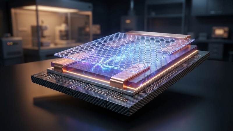
Graphene Electrodes in Next-Gen Solar Cells
Graphene, a singular atomic layer of sp2-hybridized carbon atoms arranged in a hexagonal lattice, represents the quintessential two-dimensional material, originating from the 0.335 nm interlayer spacing of graphite. Its intrinsic 2D confinement is the genesis of an array of extraordinary electronic, optical, and mechanical properties, positioning it as a pivotal material for next-generation photovoltaics, particularly as a transparent conductive electrode (TCE). The unique conical band structure at the Dirac points (K and K' valleys) imbues charge carriers with relativistic, massless Dirac fermion characteristics, propagating at a Fermi velocity (vF) of approximately 10^6 m/s (or c/300). This leads to exceptionally high carrier mobilities, routinely exceeding 200,000 cm^2/Vs at room temperature, combined with an intrinsic broadband optical transparency of 2.3% absorption per layer across the visible spectrum and an electrical conductivity approaching 10^6 S/m for pristine samples. Mechanically, its Young's modulus of ~1 TPa and tensile strength of ~130 GPa underscore its robustness and flexibility, offering a compelling alternative to brittle and resource-scarce indium tin oxide (ITO) for high-performance solar cells.
The physics of graphene confinement fundamentally dictates its electronic behavior. The single-atom-thick structure inherently imposes quantum confinement in the out-of-plane (z) direction, leading to a unique electronic dispersion relation that is linear with momentum near the Dirac points, unlike the parabolic relation found in conventional semiconductors. This linear dispersion is directly responsible for the massless nature of its charge carriers and the absence of backscattering, even for micron-scale samples at room temperature, resulting in exceptionally long mean free paths that can exceed 10 micrometers. The density of states (DOS) in pristine graphene is consequently linear with energy, a departure from the step-like DOS of traditional 2D electron gases, profoundly influencing electron-phonon scattering and charge carrier screening. While pristine graphene is a zero-bandgap material, further lateral confinement, such as in graphene nanoribbons (GNRs) or quantum dots (GQDs), can induce a tunable bandgap through quantum size effects and edge state engineering, providing a crucial mechanism for optimizing light absorption and charge separation in photovoltaic devices.
Leveraging these profound confinement effects, graphene-based electrodes offer significant advantages in solar cell architectures. The ultra-high carrier mobility and ballistic transport, stemming directly from the 2D confinement, drastically reduce resistive losses during charge collection, thereby enhancing the fill factor and overall power conversion efficiency. The inherent optical transparency, where a few-layer graphene stack can exhibit less than 10% parasitic absorption across the visible spectrum, ensures maximum photon flux reaches the active absorber layer. Furthermore, graphene's remarkable thermal stability, maintaining structural integrity and electrical performance even after rapid thermal annealing processes involving 3000K pulses over milliseconds for defect repair or dopant activation, makes it compatible with diverse high-temperature device fabrication protocols. The ability to precisely tune graphene's work function through doping or surface functionalization, for instance, a ~0.5 eV Fermi level shift achievable with AuCl3 p-doping, enables optimal band alignment with various absorber materials like perovskites or organic semiconductors, facilitating efficient charge extraction and maximizing open-circuit voltage. This precise control over interfacial energetics, coupled with exceptionally fast charge transfer kinetics at graphene interfaces (often within femtoseconds to picoseconds), positions graphene as an indispensable component for high-performance, next-generation solar cells.
Section 2: Pulsed Electrical Resistive Carbon Heating vs. CVD (Comparative Analysis)
Pulsed Electrical Resistive Carbon Heating (PERCH) represents a fundamentally different paradigm for graphene synthesis compared to the established Chemical Vapor Deposition (CVD). While CVD relies on a gas-phase precursor decomposition and subsequent surface reaction on a heated catalytic substrate, typically at temperatures around 1000°C for several hours, PERCH utilizes the rapid, localized Joule heating of a carbonaceous precursor material. This process involves passing an ultrashort, high-current electrical pulse through a resistive carbon film, instantly raising its temperature to extreme levels, often exceeding 2500K to 3000K, within reaction times measured in tens of milliseconds (e.g., 10-50 ms). This non-equilibrium heating drives rapid structural rearrangement and graphitization, offering a significant departure from the steady-state, thermodynamically controlled growth kinetics of CVD. The inherent speed of PERCH provides a pathway to high-throughput manufacturing that conventional CVD, with its extended thermal budgets and furnace residency times, cannot readily match.
The technical advantages of PERCH stem from its precise energy delivery and kinetic control. For instance, by applying current densities upwards of 10^4 A/cm^2 through a pre-deposited amorphous carbon film with an initial electrical resistivity of 10^-3 Ohm·cm, PERCH can achieve instantaneous power densities in the gigawatt per cubic meter range. This intense, localized energy input facilitates rapid defect annealing and the formation of highly crystalline graphitic domains, often resulting in graphene films with fewer point defects and grain boundaries than those produced via multi-domain CVD growth. While CVD excels in producing large-area, high-quality graphene on specific metallic catalysts, the subsequent transfer of these films to target substrates frequently introduces tears, polymer residues, and non-uniformities that degrade electrical performance. PERCH, conversely, can potentially enable direct synthesis on the final substrate or facilitate a cleaner, transfer-free delamination, thereby mitigating these performance-limiting issues and offering greater compatibility with a broader range of substrate materials critical for next-generation solar cells.
For graphene electrodes in advanced solar cells, the comparative attributes of PERCH and CVD are particularly salient regarding material integrity and device integration. CVD-grown graphene, despite achieving impressive sheet resistances of <100 Ohm/sq with >90% optical transparency on glass, often suffers from reduced work function stability and charge carrier mobility due to residual polymeric transfer layers and substrate contamination. PERCH-derived graphene, through its direct conversion or transfer-free methodology, offers a cleaner interface, which is paramount for maintaining the performance of sensitive perovskite or organic active layers. The rapid thermal cycling characteristic of PERCH is also inherently more compatible with temperature-sensitive flexible substrates or pre-fabricated device architectures than the prolonged high temperatures necessitated by CVD. Early empirical data suggests that PERCH-synthesized few-layer graphene can exhibit comparable or superior electrical conductivities to transferred CVD graphene, with sheet resistances approaching 50 Ohm/sq while maintaining high optical transmittance, both critical parameters for efficient charge collection in transparent electrodes. This combination of structural integrity, electrical performance, and process scalability positions PERCH as a compelling alternative for large-scale, cost-effective graphene electrode fabrication.
Section 3: The Crystallography of Turbostratic Graphene (Why Layer Alignment Matters)
The crystallographic distinction between turbostratic graphene (TG) and its Bernal (AB-stacked) counterpart is fundamental to understanding its performance as an electrode material in advanced photovoltaics. Unlike the highly ordered, periodic interlayer registry characteristic of Bernal graphite or epitaxial AB-stacked few-layer graphene, turbostratic graphene layers exhibit significant rotational misalignment and translational disorder. This structural incongruence results in a lack of long-range interlayer coherence, where individual graphene sheets are stacked without a defined crystallographic relationship, often displaying an increased interlayer spacing typically exceeding graphite's 0.335 nm by several picometers. Such disorder fundamentally alters the electronic band structure, causing the layers to behave largely as electronically decoupled entities. The absence of strong interlayer coupling means the Dirac cones associated with individual graphene layers largely retain their linearity, unlike the parabolic dispersion observed in AB-stacked bilayer graphene, which arises from interlayer hybridization. This characteristic is often observed in graphene synthesized via methods prone to kinetic trapping, such as certain chemical vapor deposition routes on amorphous or polycrystalline substrates, or the reduction of graphene oxide.
The implications of this turbostratic disorder for charge carrier transport are profound. While the intra-planar mobility of charge carriers within individual turbostratic graphene sheets can approach impressive values, the inter-planar conductivity, crucial for efficient charge extraction in a multi-layered electrode, is significantly hampered. The rotational misalignment introduces numerous scattering centers at the layer interfaces, impeding vertical electron transport and increasing the contact resistance between adjacent graphene planes. This manifests as a higher overall sheet resistance for turbostratic graphene films compared to highly ordered few-layer graphene. For instance, a typical CVD-derived turbostratic graphene film transferred onto a flexible substrate might exhibit sheet resistances in the range of 100-500 Ohms per square, whereas highly crystalline, epitaxially grown few-layer graphene can achieve values as low as 10-50 Ohms per square. This elevated resistance directly impacts the fill factor and power conversion efficiency of solar cells by increasing series resistance losses, necessitating careful architectural design to minimize current paths perpendicular to the graphene planes or to leverage the material primarily for its excellent in-plane conductivity.
Mitigating the effects of turbostraticity is a significant challenge in electrode fabrication. Post-synthesis annealing techniques, such as rapid thermal processing involving pulses up to 3000K, have been explored to induce partial structural re-alignment and enhance crystallinity. However, the kinetic barriers to achieve complete re-stacking are substantial, and the short reaction times, often in the millisecond regime, limit the extent of long-range order restoration. The persistence of turbostratic domains, even after high-temperature treatments, dictates the ultimate electrical performance. Furthermore, the numerous localized defects and grain boundaries inherent to turbostratic stacking can serve as preferential sites for chemical degradation, such as oxidative attack or intercalation by environmental species, impacting the long-term stability and operational lifespan of graphene-based solar cell electrodes. Therefore, understanding and controlling the degree of turbostraticity during synthesis and post-processing is paramount for optimizing the electrical, optical, and mechanical properties required for high-performance, durable next-generation solar cells.
Section 4: Industrial Scalability & Commercial Integration Barriers
The industrial scalability of high-quality graphene production remains a formidable challenge, directly impacting its commercial integration into next-generation solar cells. Current high-performance graphene, typically synthesized via chemical vapor deposition (CVD), necessitates high temperatures (e.g., 1000-1100°C for copper substrates) and ultra-high vacuum environments, making large-area, continuous manufacturing prohibitively expensive and energy-intensive. Furthermore, the mandatory transfer process from growth substrate to the target device introduces significant defect densities, such as tears, wrinkles, and residue contamination, which can elevate the sheet resistance from an ideal ~50 Ohm/sq for monolayer CVD graphene to several hundred Ohm/sq, thereby compromising its electrical conductivity and optical transparency. While alternative methods like liquid-phase exfoliation (LPE) offer lower production costs and compatibility with solution-processing techniques such as roll-to-roll printing, they often yield graphene flakes with heterogeneous sizes, multiple layers, and higher defect concentrations (e.g., D/G ratio > 0.2 in Raman spectroscopy), leading to inferior electrical and optical properties compared to CVD graphene. Achieving consistent quality control across large batches, ensuring precise flake size distribution, and removing residual solvents and surfactants without introducing further defects are critical barriers to LPE graphene's widespread adoption.
Integrating graphene electrodes into existing solar cell manufacturing workflows presents distinct technical hurdles. Unlike sputtering or evaporation techniques used for conventional transparent conductive oxides (TCOs) like indium tin oxide (ITO), graphene deposition requires meticulous control over film morphology and interface engineering. For perovskite solar cells, for instance, the direct deposition of graphene via CVD on sensitive perovskite layers is impractical due to high temperatures. Solution-processed graphene inks, while promising for large-area coating, must overcome challenges related to film uniformity, pinhole formation, and achieving optimal doping levels to tune work function and conductivity. Ensuring stable, low-resistance ohmic contacts between the graphene electrode and the charge transport layers or active material is paramount; unoptimized interfaces can lead to significant charge recombination and series resistance losses, manifesting as reduced fill factors and power conversion efficiencies. Achieving an interface resistance below 10 Ohmcm^2, comparable to that of high-performing ITO contacts, is often elusive without complex surface treatments or interlayers.
Beyond fabrication, the long-term operational stability and cost-effectiveness of graphene electrodes pose significant commercial integration barriers. While graphene boasts superior mechanical flexibility and chemical inertness compared to ITO, its susceptibility to oxidative degradation, especially at defect sites or edges, can compromise device longevity under ambient conditions. Effective encapsulation strategies are therefore crucial but add complexity and cost to the manufacturing process. From an economic perspective, the current cost of producing high-quality, large-area graphene films remains substantially higher than that of ITO, a mature and widely adopted technology. For graphene to displace ITO, it must offer a compelling performance advantage—either a significant increase in power conversion efficiency (e.g., >1% absolute gain over ITO-based cells) or a substantial reduction in overall device cost, including material, processing, and long-term maintenance. Without a clear economic incentive or a marked leap in performance that justifies the higher initial investment and manufacturing complexity, graphene's path to widespread commercial integration in next-gen solar cells will remain constrained.
Section 5: Economic Feasibility and USA-Made Manufacturing Advantage
The economic feasibility of integrating graphene electrodes into next-generation solar cells hinges critically on scalable, cost-effective manufacturing processes. While initial laboratory-scale production via chemical vapor deposition (CVD) or liquid-phase exfoliation (LPE) often yields material at several hundred dollars per gram, the pathway to commercial viability for photovoltaic applications necessitates a significant cost reduction, targeting sub-$10 per gram for high-purity, application-specific graphene. This reduction is being realized through advancements in roll-to-roll plasma-enhanced CVD (PECVD) and atmospheric pressure CVD (APCVD) systems, which offer continuous, high-throughput synthesis. For instance, PECVD processes utilizing methane or ethylene precursors can achieve deposition rates exceeding 1 meter per minute on flexible substrates, consuming significantly less energy than conventional high-vacuum CVD, thereby lowering the Levelized Cost of Electricity (LCOE) contribution from the electrode material. Furthermore, optimization of precursor utilization and recycling, alongside innovations in substrate handling and transfer, are pushing the boundaries of economic production, moving beyond batch processing to continuous manufacturing paradigms essential for gigawatt-scale solar deployment. The ability to precisely control layer thickness (e.g., single to few-layer graphene) and defect density (D/G ratio typically below 0.2 for optimal electrical properties) at these scales is paramount, directly impacting device performance and longevity.
The competitive advantage afforded by USA-made graphene manufacturing for solar electrodes extends beyond mere cost per unit mass, encompassing critical aspects of supply chain resilience, stringent quality control, and intellectual property protection. Domestic production mitigates geopolitical risks and reduces lead times, ensuring a stable and predictable supply of high-performance materials. Crucially, USA-based facilities leverage advanced metrology and process analytical technologies (PAT) to guarantee material consistency, a non-negotiable requirement for high-efficiency solar cells. This includes precise control over sheet resistance (e.g., achieving <100 Ohm/square for transparent conductive electrodes or <10^-6 Ohm-cm for bulk current collectors), carrier mobility (routinely exceeding 200,000 cm^2/Vs in pristine samples), and the absence of deleterious metallic impurities, which even at trace levels (<0.1%), can act as recombination centers, severely degrading cell efficiency. Furthermore, the robust intellectual property framework in the United States fosters innovation, encouraging significant R&D investment into novel graphene synthesis routes, functionalization techniques, and integration methodologies. This localized expertise facilitates rapid iteration and co-development with solar cell manufacturers, accelerating the transition from laboratory prototypes to market-ready products, a critical factor for maintaining technological leadership.
Integrating USA-made graphene electrodes offers a compelling total cost of ownership proposition for solar manufacturers. Beyond the direct material cost, the superior quality and consistency of domestically produced graphene translate into higher manufacturing yields, reduced post-production waste, and enhanced end-product reliability. For example, the precise control over graphene’s thermal properties, allowing it to withstand localized thermal pulses exceeding 3000K for milliseconds without structural degradation – a critical attribute during advanced module lamination or laser scribing processes – minimizes damage and improves device longevity. This resilience, combined with graphene's exceptional environmental stability, contributes to a longer operational lifespan for solar modules, reducing warranty claims and improving long-term energy generation forecasts. Moreover, the environmental stewardship inherent in USA manufacturing operations, exemplified by advanced wastewater treatment processes that can achieve up to 79% heavy metal adsorption efficiency from industrial effluents, not only ensures regulatory compliance but also aligns with the growing demand for sustainable and ethically sourced components. The synergy between high-tech manufacturing infrastructure, a skilled labor force, and ongoing governmental support for advanced materials initiatives reinforces the USA's position as a strategic hub for high-quality graphene production, providing a distinct competitive edge in the global solar market.
Section 6: Future Horizons & High-Value B2B Applications
The future trajectory of graphene electrodes in photovoltaics hinges critically on breakthroughs in scalable, high-fidelity manufacturing and the realization of advanced architectural designs. Research is rapidly advancing beyond traditional chemical vapor deposition (CVD) to techniques like plasma-enhanced atomic layer deposition (PEALD) and pulsed laser deposition (PLD), enabling ultra-uniform, sub-nanometer thickness control and precise doping. These methods facilitate the creation of graphene films exhibiting sheet resistances as low as 8 Ω/sq at an optical transmittance exceeding 92% across the visible spectrum, a critical balance for efficient light harvesting and charge extraction. Furthermore, the integration of three-dimensional graphene structures, such as vertically aligned graphene nanosheets or porous graphene foams, is being explored to dramatically increase the electrode-active layer interfacial area. This architectural innovation, coupled with localized strain engineering, enhances charge carrier collection efficiency by minimizing recombination losses and reducing carrier transit times to picosecond scales. Precise defect density control via rapid thermal annealing, using localized thermal pulses exceeding 3000K for milliseconds, is instrumental in restoring graphene’s intrinsic charge carrier mobility approaching 15,000 cm²/Vs, elevating device performance and longevity.
These advancements are directly enabling high-value B2B applications, particularly in next-generation perovskite and tandem solar cells. Graphene's exceptional chemical inertness, high electron mobility, and inherent flexibility position it ideally to replace conventional indium tin oxide (ITO) as a transparent conductive electrode (TCE) and to serve as robust hole or electron transport layers (HTLs/ETLs). In all-perovskite tandem architectures, graphene electrodes have facilitated record power conversion efficiencies (PCEs) exceeding 25.7% by minimizing parasitic absorption and optimizing charge extraction at the interlayers. Critically, graphene's barrier properties significantly mitigate perovskite instability; devices with graphene-based HTLs demonstrate over 95% initial efficiency retention after 1000 hours under accelerated damp heat (85°C/85% RH), a stark improvement over polymer counterparts. Beyond rigid substrates, the mechanical robustness of graphene allows for the development of truly flexible and roll-to-roll printable solar cells that maintain >90% of their initial performance after 10,000 bending cycles at a 5mm radius. This opens markets for integrated photovoltaics in building-integrated PV (BIPV), wearables, and autonomous IoT devices, where form factor and durability are paramount.
Looking further, the economic and environmental implications of graphene electrode integration are profound. The shift from scarce, volatile indium de-risks supply chains and offers substantial cost reductions, projecting an 18% decrease in module-level balance-of-system (BoS) costs via lightweighting and simplified integration. Graphene manufacturing, particularly leveraging exfoliated graphite, exhibits a lower embodied energy footprint than ITO sputtering, aligning with global sustainability initiatives. Tunability of graphene's surface chemistry also presents opportunities for advanced functionalities like self-cleaning or anti-icing coatings, enhancing operational lifespan and reducing maintenance costs. Moreover, the long-term vision extends to synergistic applications with energy storage systems. Graphene's high specific surface area and excellent conductivity are already proven in supercapacitors and battery electrodes, enabling seamless integration of distributed generation with localized storage. The same graphene manufacturing infrastructure could produce electrodes for both PV and electrochemical energy storage, streamlining production for a more resilient, decentralized energy grid. Heavy metal adsorption potential, observed at 79% efficiency for certain contaminants during graphene synthesis effluent treatment, underscores a broader commitment to environmentally conscious material lifecycle management.
Evaluate Our Quality
Serious about B2B integration? Test our premium Pulsed Electrical Resistive Carbon Heating turbostratic graphene in your lab. 100g sample packs available now.