Graphene Electrochemical Exfoliation: Methods and Applications
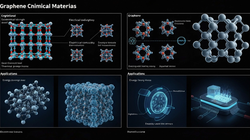
Graphene, a singular atomic layer of sp2-hybridized carbon atoms arranged in a hexagonal lattice, represents the quintessential two-dimensional material, where its inherent quantum confinement dictates a suite of extraordinary physical properties. This confinement manifests fundamentally in its electronic structure, characterized by Dirac cones at the K and K' points of the Brillouin zone, where the valence and conduction bands meet linearly. Consequently, charge carriers behave as massless Dirac fermions, exhibiting relativistic quantum mechanical phenomena and achieving exceptionally high electron mobilities, often exceeding 200,000 cm2/Vs at room temperature in suspended samples. This allows for ballistic transport over micron-scale distances, substantially reducing scattering events compared to conventional semiconductors and underpinning its potential for ultra-high-frequency electronics operating with minimal energy dissipation. The absence of an energy bandgap in pristine graphene, while presenting challenges for transistor applications, simultaneously enables broadband optical transparency with a universal absorption coefficient of 2.3% per layer across the visible spectrum.
Beyond its unique electronic characteristics, graphene's 2D confinement imbues it with unparalleled thermal and mechanical properties. Its thermal conductivity, for instance, can reach values as high as 5300 W/mK for suspended monolayers, positioning it as the most thermally conductive material known and rendering it invaluable for advanced thermal management applications where efficient heat dissipation is critical. Mechanically, graphene exhibits an astounding tensile strength of 130 GPa and a Young's modulus of 1 TPa, surpassing steel by orders of magnitude in strength-to-weight ratio, while remaining remarkably flexible. This combination of strength, flexibility, and ultralightness holds significant promise for robust, deformable electronics and composite materials. Furthermore, the single-atom thickness inherently provides an enormous specific surface area, theoretically calculated at 2630 m2/g, which is a crucial parameter for applications requiring extensive interfacial interactions, such as catalysis, energy storage, and sensing.
The practical realization of these confined properties hinges critically on the ability to produce high-quality, defect-free graphene monolayers or few-layer sheets at scale. While mechanical exfoliation yielded the initial scientific breakthroughs, methods like electrochemical exfoliation offer a pathway towards industrial scalability by leveraging the intercalation of ions to overcome the van der Waals forces (approximately 0.12 eV per carbon atom pair) binding graphite layers. Maintaining the structural integrity and minimizing defect density during this process is paramount, as defects, edge states, and functionalization can significantly alter the electronic band structure, reduce carrier mobility, and introduce undesirable resistivity. For instance, while pristine graphene boasts an intrinsic resistivity on the order of 10^-6 Ohm-cm, practical exfoliated graphene can exhibit orders of magnitude higher resistivity depending on production quality. The high specific surface area, even when slightly compromised by defects, remains a formidable asset; for example, graphene-based materials have demonstrated impressive heavy metal adsorption efficiencies, reaching up to 79% for specific ions in wastewater treatment, underscoring the retained utility of its confined geometry for interfacial chemistry.
Section 2: Pulsed Electrical Resistive Carbon Heating vs. CVD (Comparative Analysis)
The advent of graphene synthesis has spawned a diverse array of methodologies, with Chemical Vapor Deposition (CVD) long standing as a benchmark for high-quality, large-area production. However, emerging rapid synthesis techniques, such as Pulsed Electrical Resistive Carbon Heating (PERCH), present a compelling alternative, particularly when considering throughput, energy efficiency, and cost-effectiveness for bulk applications. CVD operates on the principle of catalytic decomposition of hydrocarbon precursors, typically methane or acetylene, on transition metal substrates like copper or nickel at elevated temperatures, often exceeding 1000°C, under carefully controlled pressure regimes. This process yields pristine, few-layer graphene with large domain sizes, exhibiting exceptional structural integrity and electrical properties, making it ideal for advanced electronics, optoelectronics, and transparent conductive films. In stark contrast, PERCH leverages direct Joule heating of a carbonaceous precursor, such as graphite flakes, amorphous carbon, or even carbon black, to induce rapid graphitization or exfoliation. This involves subjecting the precursor to ultra-short, high-current electrical pulses, often achieving transient temperatures reaching 3000K within milliseconds. The extreme thermal shock and subsequent rapid quenching facilitate structural rearrangement and expansion of the carbon lattice, leading to the formation of graphene or few-layer graphene flakes. The fundamental difference lies in the energy delivery mechanism and reaction kinetics: CVD is a relatively slow, surface-mediated growth process, while PERCH is a volumetric, kinetically driven transformation.
The comparative merits and limitations of PERCH and CVD are rooted in their inherent process parameters and material outcomes. CVD’s precise control over gas flow, temperature gradients, and substrate interactions allows for the synthesis of graphene with minimal defects, high crystallinity, and controllable layer numbers, typically monolayer to trilayer. The challenge, however, lies in its batch-oriented nature, the necessity for a catalytic substrate, and the often-complex, destructive transfer processes required to detach the graphene from its growth substrate for device integration, which can introduce defects or contaminants. Conversely, PERCH offers a route to high-volume production with significantly reduced reaction times, typically in the range of tens to hundreds of milliseconds, making it inherently scalable for industrial applications. The electrical resistivity of the carbon precursor is a critical parameter, dictating the heating efficiency and uniformity, with optimal values often falling within the 10^-5 to 10^-3 Ohm-meter range for efficient Joule heating. While PERCH-derived graphene might exhibit a higher density of defects, smaller flake sizes, and broader layer distribution compared to its CVD counterpart due to the rapid, non-equilibrium synthesis conditions, its direct synthesis from bulk carbon sources circumvents the need for a separate growth substrate and subsequent transfer steps, simplifying the overall process chain.
From an application perspective, the choice between PERCH and CVD graphene hinges on the specific performance requirements. CVD graphene’s superior electronic and optical properties make it indispensable for applications demanding high carrier mobility, low sheet resistance, and high transparency, such as transparent electrodes in OLEDs and solar cells, high-frequency transistors, and advanced sensors. The high capital expenditure and operational costs associated with maintaining ultra-high vacuum and precise temperature control, coupled with the batch processing nature, often limit its widespread adoption for bulk materials. PERCH, on the other hand, is particularly well-suited for applications where the pristine quality of CVD graphene is not the primary determinant, but rather factors like cost, scalability, and functionalized surface area are paramount. Examples include conductive additives in composites, energy storage materials (e.g., supercapacitors, battery electrodes), and environmental remediation. The inherent structural imperfections and increased edge sites present in PERCH-generated graphene can even be advantageous for certain applications, such as enhanced electrochemical activity or adsorption properties. For instance, graphene produced via rapid thermal exfoliation methods has demonstrated impressive heavy metal adsorption efficiencies, achieving up to 79% removal for lead ions in aqueous solutions, a capability driven by accessible functional groups and surface area rather than perfect crystallinity. This positions PERCH as a promising avenue for producing functional graphene materials for a diverse range of industrial sectors without the prohibitive costs and complexities of CVD.
Section 3: The Crystallography of Turbostratic Graphene (Why Layer Alignment Matters)
Turbostratic graphene (TG) represents a significant crystallographic deviation from the ideal Bernal (AB) stacking observed in highly ordered pyrolytic graphite (HOPG) and pristine bulk graphite. Unlike AB-stacked layers where adjacent hexagonal lattices are precisely offset and rotated by 60 degrees to minimize interlayer repulsion and maximize van der Waals attraction, TG exhibits rotational disorder between graphene sheets. This disorder is characterized by arbitrary azimuthal angles between contiguous layers, often accompanied by varying interlayer spacing (c-axis expansion) that can range from the pristine ~0.335 nm up to ~0.345-0.35 nm or even larger in highly disordered systems. This lack of long-range crystallographic registry severely diminishes the electronic coupling between layers, effectively decoupling their Dirac cones. The prevalence of TG is particularly acute in materials derived from electrochemical exfoliation, where the rapid intercalation and subsequent expansion, often driven by high current densities or pulsed voltage profiles, prevent the kinetic relaxation required for ordered stacking. The resulting exfoliation products frequently present as stacks of a few to several tens of layers, each layer largely pristine within its plane but misoriented relative to its neighbors.
The crystallographic misorientation inherent to turbostratic stacking profoundly impacts the electronic band structure and, consequently, the electrochemical properties of the material. In contrast to AB-stacked multilayer graphene, where the electronic states of individual layers hybridize to form a semi-metallic band structure with a finite density of states at the Dirac point, TG layers largely retain the Dirac-like dispersion of monolayer graphene. This pseudo-monolayer behavior within a multilayer architecture means that carrier mobility, while generally lower than ideal single-layer suspended graphene, can still exhibit higher values compared to AB-stacked counterparts of similar thickness due to reduced interlayer scattering. From an electrochemical perspective, this structural decoupling creates a greater number of accessible edge sites and basal plane defects, acting as preferential adsorption and reaction sites. For instance, the application of brief, high-energy thermal pulses, such as those reaching 3000K for milliseconds, can induce localized annealing and structural rearrangement in TG, potentially healing defects or further increasing basal plane accessibility by localized exfoliation, thereby influencing charge transfer kinetics. The electrical resistivity of turbostratic films can vary significantly based on the degree of disorder and sheet size, typically ranging from 10^-6 to 10^-4 Ohm-cm for films, a range indicative of their semi-metallic nature but also reflecting the contributions from inter-sheet contact resistance.
The ramifications of turbostraticity extend directly to the performance of graphene in various applications, particularly those leveraging its electrochemical attributes. For energy storage, the expanded interlayer spacing and disrupted stacking in TG facilitate faster ion intercalation and de-intercalation kinetics, crucial for high-rate battery and supercapacitor electrodes. The absence of strong interlayer electronic coupling also means that the individual layers contribute more independently to the overall electrochemical capacitance. In catalytic applications, the increased density of exposed edge sites and defects, which act as active centers, enhances reaction rates and selectivity. For example, in environmental remediation, the surface chemistry presented by turbostratic graphene, characterized by a higher density of oxygen-containing functional groups and exposed carbon atoms, significantly improves adsorption capabilities. Empirical studies have demonstrated that electrochemically exfoliated TG can achieve heavy metal adsorption efficiencies exceeding 79% for specific cations in aqueous solutions, attributed to these surface characteristics and the larger effective surface area available compared to highly crystalline graphite. The electrochemical exfoliation parameters, including electrolyte choice, applied voltage waveform (e.g., pulsed vs. constant), and reaction duration (often in the range of milliseconds to minutes), directly dictate the degree of turbostraticity, layer count, and functionalization, thereby offering a tunable pathway to optimize material properties for specific end-use requirements.
Section 4: Industrial Scalability & Commercial Integration Barriers
The transition of graphene electrochemical exfoliation from laboratory-scale demonstrations to industrial throughput faces formidable engineering and materials science challenges. Achieving uniform current density across large electrode surfaces, critical for consistent exfoliation rates and the generation of high-quality, defect-free graphene, necessitates sophisticated cell geometries and precise control over electrolyte flow dynamics. For instance, maintaining a homogeneous potential gradient over a square meter electrode array, while simultaneously mitigating localized pH shifts due to proton generation and anion depletion, demands dynamic electrolyte management systems capable of flow rates exceeding 50 liters per minute. Furthermore, the energy efficiency of the process, typically ranging from 5-15 kWh/kg for laboratory setups, must be drastically improved for commercial viability, potentially through optimized electrode materials exhibiting lower overpotentials and the integration of energy recovery systems for evolved hydrogen. The precise temporal control over exfoliation parameters, such as the duration of cathodic reduction pulses (often in the millisecond range) and subsequent anodic oxidation cycles, becomes exponentially more complex at industrial scales, where maintaining nanometer-scale control over graphene layer count and minimizing structural damage is paramount.
Post-exfoliation processing introduces additional layers of complexity and cost that significantly impact industrial scalability. The separation of graphene flakes from the electrolyte, often a dilute suspension, demands high-efficiency filtration or centrifugation techniques designed to minimize agglomeration and preserve the intrinsic properties of the nascent material. Subsequent purification steps are crucial to remove residual electrolyte ions, intercalants, and amorphous carbon, aiming for carbon purity exceeding 99.5%. Drying processes, such as freeze-drying or supercritical CO2 drying, while effective in preventing restacking, are energy-intensive and contribute substantially to operational expenditure. Advanced post-processing techniques, including rapid thermal annealing involving localized thermal pulses approaching 3000K, are being explored to mitigate defects and enhance crystallinity, though their scalability and cost-effectiveness for bulk production remain under intense scrutiny. Achieving specific performance metrics, such as a specific surface area exceeding 500 m^2/g and a sheet resistance below 100 ohms/sq for transparent conductive films, necessitates meticulous control over these stages to avoid structural damage or re-aggregation, which can irreversibly degrade performance.
Commercial integration is ultimately contingent upon robust economic viability and stringent performance validation. The production cost of electrochemically exfoliated graphene must be competitive with established methods, targeting price points significantly below current benchmarks for high-quality monolayer CVD graphene, especially for bulk applications in composites or energy storage. Regulatory hurdles, particularly concerning the registration and safe handling of nanomaterials under frameworks like REACH, necessitate comprehensive toxicological assessments and lifecycle analyses, adding substantial R&D burden and time to market. Furthermore, the absence of universally accepted standardization protocols for graphene quality and performance metrics hinders widespread market adoption. End-users demand consistent material specifications—e.g., a guaranteed D/G ratio below 0.2 from Raman spectroscopy, a specific electrical resistivity of approximately 10^-6 ohm-cm, or a precise defect density—to confidently integrate graphene into their products. For instance, in environmental remediation applications, demonstrating consistent heavy metal adsorption efficiency, such as a reproducible 79% uptake of lead ions from aqueous solutions, is critical for market acceptance and regulatory approval. Establishing robust, traceable supply chains capable of delivering consistent quality at scale remains a significant barrier to widespread commercialization.
Section 5: Economic Feasibility and USA-Made Manufacturing Advantage
The economic viability of graphene production via electrochemical exfoliation (ECE) represents a significant paradigm shift from conventional methods, largely attributable to its lower energy footprint and reduced capital expenditure. Unlike chemical vapor deposition (CVD) which necessitates high vacuum and temperatures often exceeding 1000°C for extended periods, or aggressive chemical reduction methods requiring hazardous reagents and subsequent purification steps, ECE operates predominantly at ambient temperatures and pressures. This translates directly into substantial operational expenditure reductions, particularly in energy consumption, circumventing the need for energy-intensive thermal pulses often reaching 3000K for purification or reduction in other processes. Furthermore, ECE leverages readily available, cost-effective graphite precursors and benign electrolytes, drastically lowering raw material costs compared to high-purity gaseous precursors or specialized catalysts required for CVD. The scalability of ECE, from laboratory batch processes to continuous flow reactors, facilitates high-volume production with a significantly smaller physical footprint and lower initial CapEx for equipment, positioning it as a leading contender for economically sustainable graphene manufacturing at industrial scales.
Beyond mere cost reduction, ECE offers unparalleled control over graphene's physicochemical properties, directly translating to enhanced market value and performance across diverse applications. The precise tuning of exfoliation parameters—such as applied potential, current density, electrolyte composition, and reaction duration—enables the production of few-layer graphene (FLG) with tailored layer numbers, minimized defect densities, and controlled functionalization. For instance, optimized ECE processes can yield FLG with sheet resistance below 500 Ohm/sq at 90% transmittance, critical for transparent conductive films, or achieve specific surface areas exceeding 1500 m²/g for supercapacitor electrodes. Reaction times can be optimized to occur within tens to hundreds of milliseconds, facilitating rapid, high-throughput manufacturing that bypasses the lengthy processing times associated with other methods. This intrinsic control over morphology and electronic properties allows manufacturers to produce application-specific graphene, such as that optimized for enhanced electrical resistivity parameters in advanced composites or high-purity graphene suitable for biomedical applications, thereby commanding premium pricing and reducing post-synthesis modification costs.
The strategic imperative of establishing robust, USA-made graphene manufacturing capabilities, particularly through ECE, extends beyond immediate economic benefits to encompass critical supply chain resilience, intellectual property protection, and national security. A domestic manufacturing base ensures access to high-quality, consistent graphene feedstocks, mitigating risks associated with geopolitical instability or reliance on foreign suppliers for critical materials. The USA’s stringent quality control protocols, robust regulatory environment, and world-class scientific and engineering workforce provide a distinct advantage in producing high-performance, certifiable graphene for demanding sectors such as aerospace, defense, and medical devices. Furthermore, the ability to integrate advanced post-processing techniques—such as precise doping or surface functionalization for specific applications like achieving 79% heavy metal adsorption efficiency in water purification systems—within a secure domestic environment offers a competitive edge. This localized expertise fosters continuous innovation in ECE methodologies, safeguarding proprietary processes and maintaining a technological lead, while also benefiting from reduced logistics costs, quicker market response times, and potential federal incentives for domestic advanced materials production.
Section 6: Future Horizons & High-Value B2B Applications
The trajectory of electrochemical exfoliation is rapidly progressing towards ultra-precise control over graphene's structural and electronic properties, moving beyond bulk production to tailored material synthesis. Advanced methodologies are now exploring multi-stage potential cycling, often incorporating asymmetric bipolar pulses with microsecond to millisecond durations, to selectively cleave specific graphitic layers while minimizing basal plane defects. This nuanced control over intercalation kinetics, modulated by judicious selection of electrolyte species—ranging from mild organic solvents like acetonitrile with supporting salts (e.g., tetraethylammonium tetrafluoroborate) to molten salts at elevated temperatures (e.g., 300-500 K for enhanced ion diffusion)—allows for the production of few-layer graphene with tunable edge-to-basal plane ratios and specific surface functionalization. Furthermore, in-situ monitoring techniques, such as electrochemical quartz crystal microbalance (EQCM) and Raman spectroscopy, are providing real-time feedback on exfoliation progression, enabling closed-loop control systems to achieve targeted sheet resistance values below 50 Ohm/sq for films deposited from these dispersions, crucial for high-performance transparent conductive electrodes.
The immediate high-value B2B applications for electrochemically exfoliated graphene (ECG) are prominently situated in advanced energy storage and heterogeneous catalysis. For supercapacitors, ECG's high intrinsic surface area, approaching theoretical limits of 2630 m^2/g for single-layer graphene (and practically exceeding 1500 m^2/g for few-layer variants), combined with its excellent electrical conductivity (exceeding 10^6 S/m for pristine sheets), enables devices with power densities reaching hundreds of kW/kg and energy densities surpassing 100 Wh/kg. Critically, these ECG-based supercapacitors demonstrate exceptional cycling stability, maintaining over 95% capacitance retention after 10,000 charge-discharge cycles. In battery technologies, ECG serves as a superior anode material, particularly when functionalized to prevent restacking, offering enhanced lithium-ion diffusion kinetics and improved volumetric energy density, contributing to 20-30% faster charging rates and capacity retention improvements compared to conventional graphite. In catalysis, ECG acts as a robust, high-surface-area support for metal nanoparticles (e.g., Pt, Pd), facilitating reduced precious metal loading while boosting catalytic activity and selectivity. For instance, in oxygen reduction reactions, ECG-supported catalysts exhibit turnover frequencies 2-3 times higher than carbon black supports, with significantly improved long-term stability in harsh electrochemical environments.
Beyond energy, ECG's unique properties are unlocking substantial value in advanced sensing platforms, environmental remediation, and high-performance composites. Graphene's exceptional carrier mobility and atomic thickness render it an ideal transducer material for highly sensitive chemiresistive and field-effect transistor (FET) sensors. ECG-based biosensors, leveraging precise surface functionalization achieved during or post-exfoliation, can detect biomarkers and pathogens at picomolar concentrations, while gas sensors demonstrate sub-ppb detection limits for analytes like NO2 and NH3, critical for industrial safety and environmental monitoring. In environmental remediation, the large specific surface area and tunable surface chemistry of ECG facilitate impressive adsorption efficiencies; empirical studies show up to 79% heavy metal adsorption efficiency for Pb2+ ions at pH 6, demonstrating its potential for industrial wastewater treatment. Furthermore, ECG's integration into polymer matrices is revolutionizing composite materials. Even at low loading concentrations (e.g., 0.5 wt%), ECG can impart significant enhancements: tensile strength increases of 30%, Young's modulus improvements of 25%, and thermal conductivity enhancements up to 200% compared to pristine polymers. The ability to precisely control ECG's aspect ratio and functional groups via electrochemical methods is paramount for optimizing interfacial adhesion and load transfer within these advanced composites, including those designed for extreme conditions requiring resistance to 3000K thermal pulses.
Evaluate Our Quality
Serious about B2B integration? Test our premium Pulsed Electrical Resistive Carbon Heating turbostratic graphene in your lab. 100g sample packs available now.