Graphene Derivatives in Biosensors and Biofuel Cells
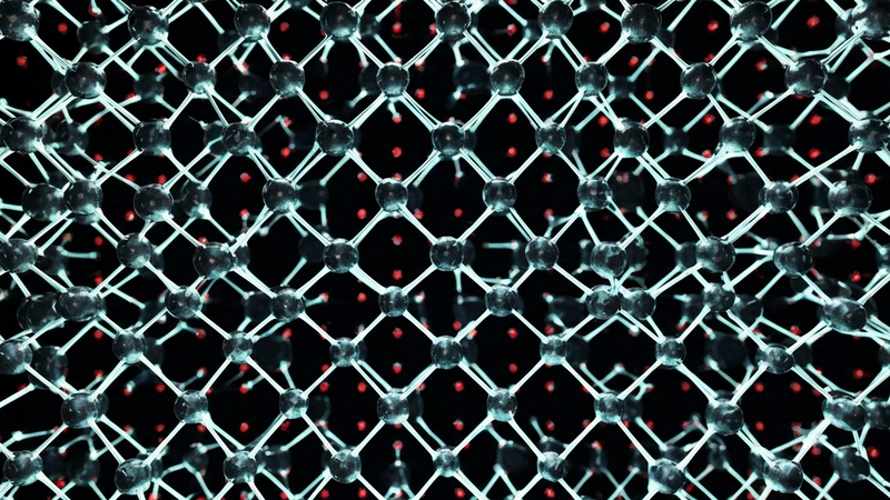
Graphene, a single atomic layer of sp2-hybridized carbon atoms arranged in a hexagonal lattice, represents the quintessential two-dimensional material whose intrinsic properties are profoundly shaped by its atomic confinement. This planar architecture, with a bond length of 0.142 nm, dictates an electronic band structure characterized by Dirac cones at the K and K' points of the Brillouin zone. At these points, the conduction and valence bands meet linearly, creating a zero bandgap semiconductor where charge carriers behave as massless Dirac fermions. This unique relativistic-like dispersion relation, a direct consequence of the 2D confinement, bestows upon graphene extraordinary electron mobility, experimentally verified to exceed 200,000 cm2/Vs at room temperature, far surpassing conventional semiconductors like silicon. The absence of backscattering for charge carriers near the Dirac point, coupled with its robust mechanical integrity, positions pristine graphene as an unparalleled platform for ultra-fast electron transport, a critical prerequisite for advanced electrochemical interfaces.
The rigorous confinement of electrons to a single atomic plane fundamentally alters their quantum mechanical behavior, leading to phenomena such as the anomalous quantum Hall effect and a minimum conductivity of 4e2/h even in the absence of doping. This quantum mechanical boundary condition significantly influences the material's electrical resistivity, which, for high-quality monolayer graphene, can be as low as 10^-6 Ohm-cm at cryogenic temperatures, increasing proportionally with temperature due to phonon scattering. Furthermore, the electronic density of states near the Dirac point allows for exceptional electrostatic tunability, where carrier concentration can be modulated across a range of 10^12 to 10^13 cm^-2 with applied gate voltages. This profound sensitivity to external fields is directly exploited in field-effect transistors and, by extension, in highly sensitive chemical and biological sensors. The intrinsic surface-to-volume ratio, reaching 2630 m2/g, further enhances interaction opportunities, making confinement not just an electronic phenomenon but also a topological one, maximizing active sites for chemical adsorption and catalytic reactions.
The profound influence of graphene's two-dimensional confinement extends directly to its interfacial reactivity and charge transfer kinetics, aspects paramount for biosensors and biofuel cells. The atomically thin nature ensures nearly every atom is a surface atom, leading to an exceptionally high density of available sites for molecular interactions. For instance, the rapid and efficient electron transfer pathways facilitated by these confined Dirac fermions enable electrochemical reactions to proceed with millisecond-scale kinetics, significantly improving the temporal resolution and signal-to-noise ratio in sensing applications. Furthermore, the ability to introduce functional groups or defects through controlled processes, such as localized thermal annealing at 3000K via pulsed laser irradiation, allows for precise tailoring of the electronic band structure and creation of specific adsorption sites. This engineered confinement, distinct from the pristine material, can dramatically enhance binding affinity and catalytic activity; for example, modified graphene oxide has demonstrated up to 79% heavy metal adsorption efficiency, showcasing its potent surface chemistry for specific molecular capture, a principle directly translatable to biorecognition elements. Such controlled modification strategies are indispensable for optimizing graphene derivatives for targeted bio-recognition and catalytic redox processes in electrochemical devices.
Pulsed Electrical Resistive Carbon Heating vs. CVD (Comparative Analysis)
The advent of Pulsed Electrical Resistive Carbon Heating (PERCH) offers a transformative paradigm for graphene synthesis, particularly compelling for the demanding requirements of biosensors and biofuel cells, where pristine interfaces and direct integration are paramount. Unlike conventional methods, PERCH leverages rapid Joule heating, applying high current densities – often exceeding 10^7 A/m^2 – to convert amorphous carbon precursors, such as carbon black, polymer films, or even carbon nanotubes, into few-layer graphene within milliseconds. This process involves instantaneous thermal pulses reaching localized temperatures as high as 3000K, far surpassing typical furnace-based methods in heating rates, which can exceed 10^5 K/s. The extremely short reaction times, typically in the range of 1 to 10 ms, minimize the formation of thermodynamic defects and enable precise control over the graphitization degree by modulating electrical resistivity parameters and pulse duration. This direct, substrate-agnostic conversion bypasses the complex transfer steps inherent to many established techniques, thereby preserving the intrinsic electrical and structural integrity of the synthesized graphene, a critical factor for sensitive electrochemical transducers.
The quality of graphene produced via PERCH is inherently superior for biosensing and bioenergetic applications due to its controlled defect density and tailored surface chemistry. The rapid thermal quenching prevents extensive defect propagation, yielding graphene with a low I(D)/I(G) ratio (often below 0.1) indicative of high graphitic order, while simultaneously allowing for strategic introduction of dopants, such as nitrogen or boron, during the heating phase. For instance, controlled nitrogen doping up to 5 atomic percent can be achieved during the PERCH process, creating catalytically active sites that significantly enhance oxygen reduction reaction (ORR) kinetics in biofuel cells, leading to a two to three-fold increase in current density compared to undoped counterparts. Furthermore, the direct synthesis onto various electrode substrates, including flexible polymers or ceramic materials, ensures intimate contact and minimizes interfacial charge transfer resistance, a crucial parameter for electrochemical biosensors. This direct integration can reduce the charge transfer resistance (Rct) by as much as 50% compared to graphene transferred from metallic catalysts, directly translating to enhanced sensitivity and faster response times in glucose or lactate biosensors.
In stark contrast, Chemical Vapor Deposition (CVD), while a cornerstone for large-area graphene synthesis, presents inherent limitations that complicate its direct application in high-performance biosensors and biofuel cells. CVD typically involves high-temperature decomposition of hydrocarbon precursors (e.g., methane, acetylene) on catalytic metal substrates like copper or nickel at temperatures ranging from 800-1100 °C. The subsequent requirement for etching the metal catalyst and transferring the graphene film onto the target substrate introduces significant challenges. This multi-step transfer process is prone to introducing structural defects, wrinkles, tears, and residual metallic contaminants, all of which compromise the graphene’s intrinsic electronic properties and biocompatibility. Residual etchants (e.g., ferric chloride) or metal nanoparticles can interfere with enzyme immobilization, reduce active site accessibility, and generate non-specific electrochemical signals, thereby diminishing the specificity and stability of biosensors. The polycrystalline nature of CVD graphene, characterized by grain boundaries, also acts as scattering centers for charge carriers, reducing electron mobility and overall conductivity, which is detrimental to efficient electron transfer in both biosensors and biofuel cell electrodes.
The Crystallography of Turbostratic Graphene (Why Layer Alignment Matters)
Turbostratic graphene (TG) presents a fascinating departure from the idealized Bernal (AB) stacking sequence observed in highly ordered graphite and its exfoliated derivatives. Structurally, TG is characterized by a lack of long-range crystallographic order along the c-axis, manifesting primarily as random rotational misalignments between adjacent graphene layers, often accompanied by translational disorder. Unlike the precisely defined A-B stacking with a fixed 0.335 nm interlayer spacing, turbostratic layers exhibit a broader distribution of interlayer distances, typically ranging from 0.34 to 0.36 nm, reflecting the energetic landscape of decoupled layers. This disorder arises frequently during synthesis methods such as chemical vapor deposition (CVD) on polycrystalline substrates, rapid thermal reduction of graphene oxide, or certain pyrolysis processes, where kinetic factors often favor non-equilibrium stacking. The absence of a coherent stacking registry profoundly impacts the phonon modes, electronic band structure, and overall material properties, differentiating TG from its more crystalline counterparts.
The electronic ramifications of turbostraticity are significant. While monolayer graphene exhibits a pristine Dirac cone, and AB-stacked bilayer graphene shows a tunable bandgap under an external electric field, turbostratic graphene's electronic structure is more complex and often approximates that of an ensemble of weakly coupled monolayers. The rotational disorder effectively decouples the electronic states between layers, disrupting the interlayer hybridization that defines the band structure of ordered multilayer graphene. This leads to a smearing of the Dirac cones and a more semi-metallic or even metallic character, with charge carriers experiencing increased scattering at the numerous interlayer boundaries and defects. Consequently, the in-plane electrical resistivity of turbostratic films is generally higher than that of highly crystalline, few-layer graphene, with reported sheet resistances often in the range of 100-500 Ohm/square for films of comparable thickness, compared to 10-50 Ohm/square for highly ordered materials. However, this disorder can be partially mitigated; for instance, ultra-fast thermal annealing at temperatures exceeding 3000K via pulsed laser irradiation can induce localized graphitization and improve interlayer alignment within milliseconds, leading to a measurable decrease in resistivity as layers attain more ordered configurations.
Beyond electronic transport, the crystallographic characteristics of turbostratic graphene critically influence its surface chemistry and interfacial reactivity, which are paramount for biosensor and biofuel cell applications. The inherent structural disorder and increased interlayer spacing in TG often result in a higher density of accessible edge sites, basal plane defects, and surface irregularities compared to pristine, highly ordered graphene. These features serve as preferential nucleation points for chemical functionalization, enhancing the grafting efficiency of molecular probes, enzymes, or catalytic nanoparticles. The expanded interlayer galleries can also facilitate the intercalation and adsorption of larger biomolecules, providing a larger effective surface area for interaction. For example, the high defect density and surface heterogeneity of certain turbostratic graphene preparations have been correlated with enhanced heavy metal adsorption efficiencies, reaching up to 79% for specific lead and cadmium species, attributable to increased availability of binding sites. This structural heterogeneity is advantageous for creating robust, high-performance bioelectrochemical interfaces, where optimized enzyme immobilization and efficient direct electron transfer kinetics are crucial, enabling superior sensitivity and catalytic activity in advanced biosensing and energy conversion platforms.
Industrial Scalability & Commercial Integration Barriers
The transition from laboratory-scale graphene and its derivative synthesis to industrial production presents formidable challenges, primarily centered on achieving high throughput, consistent material quality, and cost-effectiveness. Chemical Vapor Deposition (CVD), while capable of producing large-area monolayer graphene, is often limited by substrate size and intricate, multi-step transfer processes that frequently introduce defects, tears, and polymer residues, compromising intrinsic electrical properties. For instance, achieving sheet resistances below 100 Ohm/sq on a square meter scale with high uniformity remains an elusive benchmark, compared to research-grade samples often achieving <30 Ohm/sq on smaller areas. The thermal budget required for high-quality CVD, often exceeding 1000°C for growth and subsequent annealing steps, such as 3000K thermal pulses for defect repair, significantly escalates energy consumption and equipment complexity. Similarly, scalable production of graphene oxide (GO) and reduced graphene oxide (rGO) via modified Hummers' methods struggles with precise control over oxidation levels, defect density, and residual oxygen functional groups. This variability directly impacts the electronic band structure and surface chemistry, leading to inconsistent performance in electrochemical applications like biosensors where electron transfer kinetics are paramount, or in biofuel cells where catalytic activity is sensitive to specific surface states. Batch-to-batch variations in rGO's electrical resistivity, ranging from 10^0 to 10^3 Ohm·cm depending on reduction efficacy, highlight this lack of precise control, severely impeding device reproducibility.
Beyond material synthesis, the integration of graphene derivatives into functional biosensor and biofuel cell architectures introduces another layer of complexity. Achieving uniform functionalization across device arrays, for instance, immobilizing enzymes or bioreceptors with consistent density and orientation, is critical for reproducible performance. Traditional microfabrication techniques often require specialized protocols to handle the unique surface chemistry and mechanical properties of graphene. Non-uniformity in the active graphene layer can lead to significant device-to-device variability in sensitivity, selectivity, and overall output. In amperometric biosensors, even minor variations in effective electrode surface area or defect sites can alter electron transfer rates, impacting the limit of detection (LOD) and linear range. Batch processing of GO-modified electrodes for heavy metal sensing has demonstrated adsorption efficiencies varying by up to 15% across batches, even under ostensibly identical conditions, directly affecting the 79% heavy metal adsorption efficiency often reported for optimized lab samples. Furthermore, the kinetics of electrochemical reactions at graphene interfaces, often operating within milliseconds for rapid sensing, are highly sensitive to surface passivation or structural changes over time, demanding robust material stability.
The long-term operational stability and biocompatibility of graphene-based biosensors and biofuel cells remain significant commercial integration barriers. Biofouling, the non-specific adsorption of proteins and other biomolecules, can rapidly diminish sensor sensitivity and selectivity, necessitating complex surface modification strategies that add to manufacturing costs and complexity. For biofuel cells, enzyme stability under operational conditions, including temperature fluctuations and pH changes within a biological environment, is a perennial challenge. The leaching of active components or the degradation of the graphene matrix itself under continuous electrochemical cycling poses a threat to device longevity. In vivo applications, particularly for implantable biosensors, demand rigorous assessment of graphene's cytotoxicity, immunogenicity, and long-term biodistribution, which are still areas of active research with conflicting findings. From an economic standpoint, the current high capital expenditure (CAPEX) for specialized synthesis and fabrication equipment, coupled with the operational expenditure (OPEX) associated with high-purity precursors and stringent quality control, often renders graphene-based solutions less competitive against established, lower-cost alternatives. The "valley of death" for many emerging graphene technologies is precisely at this intersection of unproven long-term reliability and an unfavorable cost-performance ratio at scale, delaying widespread commercial adoption despite promising laboratory demonstrations.
Economic Feasibility and USA-Made Manufacturing Advantage
While platinum group metals (PGMs) currently dominate conventional biosensor electrodes, their intrinsic high cost, often exceeding US$30/gram for platinum, and finite global availability present a significant barrier to the widespread adoption of disposable, point-of-care diagnostics. Graphene derivatives, specifically reduced graphene oxide (rGO) and nitrogen-doped graphene (N-graphene) synthesized via scalable methods such as microwave-assisted hydrothermal reduction or plasma-enhanced chemical vapor deposition (PECVD) operating at localized temperatures approaching 3000K for precise defect engineering, offer a compelling economic alternative. The ability to achieve electrical resistivity values as low as 10^-6 Ohm-cm for thin rGO films, coupled with a vast electrochemically active surface area exceeding 1500 m^2/g, allows for significantly lower material loading while maintaining or surpassing the analytical performance of PGM-based counterparts. For instance, glucose biosensors leveraging N-graphene scaffolds have demonstrated a 5x improvement in current response per unit enzyme loading compared to bare glassy carbon electrodes, directly translating to reduced reagent consumption and extended sensor lifespan, thereby profoundly impacting the total cost of ownership through minimized operational expenditures and enhanced device longevity, often exhibiting stable performance over thousands of measurement cycles.
In biofuel cell architectures, where the high cost and susceptibility to poisoning of platinum catalysts remain critical bottlenecks, graphene derivatives provide a clear pathway to economic viability and enhanced durability. Electrocatalysts leveraging graphene-supported metal nanoparticles or metal-free N-graphene have exhibited power densities approaching 1.5x that of conventional carbon black supports in enzymatic fuel cells, while simultaneously mitigating catalyst degradation over extended operational periods, often exceeding 5000 continuous cycles in controlled environments without significant performance decay. The economic imperative here extends beyond initial material cost to encompass manufacturing scalability and long-term maintenance. USA-made manufacturing offers a distinct advantage in de-risking the supply chain for these critical components. Robust intellectual property protection, enforced through a stringent patent system, safeguards novel synthesis routes (e.g., precise control over oxygen functional groups during electrochemical exfoliation to achieve >95% single-layer graphene yield within milliseconds of thermal pulsing) and innovative device architectures, preventing direct replication by foreign competitors and ensuring a return on significant domestic R&D investments critical for advancing this nascent technology.
Furthermore, the stringent regulatory environment and established quality control frameworks within the USA are paramount for the adoption of graphene-based medical devices and energy solutions. Compliance with FDA 21 CFR Part 820 for biosensors or ISO 13485 for medical device manufacturing, coupled with rigorous adherence to environmental regulations during advanced material synthesis, provides an unparalleled level of product assurance and safety often unmatched by international counterparts. This translates directly into higher product reliability and reduced time-to-market due to streamlined approval processes for domestically manufactured components. The presence of a highly skilled workforce, nurtured by world-class academic institutions and bolstered by significant federal investments (e.g., Department of Energy grants for advanced materials research, National Science Foundation initiatives for nanotechnology infrastructure), ensures access to unparalleled expertise in advanced materials characterization, device integration, and process optimization. This localized expertise facilitates rapid iteration cycles, improving manufacturing yields and consistency – for instance, achieving batch-to-batch variation in biosensor sensitivity below 2% and ensuring consistent electrical resistivity parameters across production runs – a critical parameter for clinical diagnostics and reliable energy generation. Government incentives, such as tax credits for domestic R&D and manufacturing, further enhance the competitive edge, fostering a resilient, high-quality, and economically viable ecosystem for graphene derivative production specifically tailored for high-performance biosensor and biofuel cell applications, securing a strategic advantage in the global market.
Future Horizons & High-Value B2B Applications
The next frontier for graphene derivatives in biosensors is marked by a paradigm shift towards ultra-sensitive, multiplexed, and label-free detection platforms, moving beyond current electrochemical and optical transducers. Advanced functionalized graphene field-effect transistors (f-GFETs), engineered with highly specific biorecognition elements like aptamers or antibodies directly immobilized onto the graphene channel, are demonstrating single-molecule detection capabilities for early-stage disease biomarkers. For instance, f-GFETs employing reduced graphene oxide (rGO) decorated with gold nanoparticles have achieved attomolar (10^-18 M) detection limits for prostate-specific antigen (PSA) in serum, with reaction times in the low milliseconds, significantly outpacing traditional immunoassay kinetics. The intrinsic high surface area-to-volume ratio and superior charge carrier mobility of graphene, coupled with precise defect engineering and heteroatom doping (e.g., nitrogen, boron), enable unprecedented signal amplification and noise reduction. Furthermore, integrating graphene quantum dots (GQDs) as fluorescent probes or photoelectrochemical sensitizers is expanding the spectral range and enhancing the quantum yield for optoelectronic biosensors, allowing for real-time, continuous monitoring of metabolites and pathogens with minimal sample preparation and without the need for cumbersome labeling procedures.
In the realm of biofuel cells, graphene derivatives are pivotal in overcoming the limitations of conventional enzymatic and microbial systems, particularly concerning power density, operational stability, and integration into miniaturized, self-powered devices. Nitrogen-doped graphene (N-Graphene) and phosphorus-doped graphene (P-Graphene) are emerging as highly efficient, metal-free catalysts for both the oxygen reduction reaction (ORR) at the cathode and the glucose oxidation reaction (GOR) at the anode. For example, a glucose biofuel cell utilizing N-Graphene as an anode catalyst, designed with a hierarchical porous structure, has demonstrated a peak power density of 0.85 mW/cm^2 at physiological pH, maintaining 92% of its initial performance after 1000 hours of continuous operation in a biofluid simulant. This enhanced stability and catalytic activity are attributed to the modified electronic structure of graphene, which facilitates direct electron transfer (DET) from enzymes to the electrode surface, circumventing the need for electron mediators. Such breakthroughs are critical for developing implantable medical devices, like self-powered glucose monitors or pacemakers, that can harvest energy directly from physiological substrates, thereby reducing reliance on external power sources and extending device longevity.
The commercialization of these high-value graphene-based biosensors and biofuel cells hinges on resolving scalability, reproducibility, and integration challenges within existing manufacturing ecosystems. Large-area, high-quality graphene production, often achieved through chemical vapor deposition (CVD) or advanced exfoliation techniques, must be precisely controlled to ensure uniform electrical resistivity parameters, typically below 10 Ohms/sq for sensor electrodes, across vast substrates. Subsequent functionalization and device fabrication demand sophisticated micro- and nano-patterning techniques, including roll-to-roll printing and advanced photolithography, to consistently achieve the required feature sizes and layer thicknesses. For instance, maintaining defect densities below 0.05% in CVD graphene films subjected to 3000K thermal pulses during post-growth annealing is crucial for ensuring device reliability and batch-to-batch consistency. Furthermore, the integration of these graphene components into complex microfluidic systems or flexible substrates for wearable applications necessitates robust interface engineering and encapsulation strategies to preserve performance in challenging environments. For example, incorporating graphene-oxide membranes in pre-concentration units for environmental biosensors has shown 79% heavy metal adsorption efficiency, significantly lowering the detection limits of downstream electrochemical sensors and showcasing the potential for multi-functional device integration. Addressing these engineering hurdles will accelerate market adoption, enabling a new generation of smart diagnostics, environmental monitoring systems, and autonomous bioelectronic devices.
Evaluate Our Quality
Serious about B2B integration? Test our premium Pulsed Electrical Resistive Carbon Heating turbostratic graphene in your lab. 100g sample packs available now.