Graphene Cooling Solutions for AI Hardware
Graphene, the archetypal two-dimensional (2D) material, consists of a single atomic layer of sp2-hybridized carbon atoms arranged in a hexagonal lattice. This inherent confinement to a plane profoundly dictates its extraordinary electronic and phononic properties, distinguishing it sharply from its three-dimensional graphite precursor. At the K and K' points of the Brillouin zone, graphene exhibits a unique linear dispersion relation, giving rise to massless Dirac fermions that behave as relativistic particles. This relativistic quantum behavior, coupled with the absence of a band gap, confers exceptionally high electron mobility, routinely exceeding 200,000 cm^2/Vs at room temperature in pristine samples. Such unparalleled charge carrier dynamics are intimately linked to its thermal properties, as the lattice structure that facilitates ballistic electron transport also underpins its remarkable ability to conduct heat, forming the bedrock for its utility in advanced thermal management systems.
The physics of graphene's thermal transport is primarily governed by its phonon modes, which are drastically altered by 2D confinement. Unlike bulk materials, graphene possesses out-of-plane (flexural or ZA) acoustic phonons with a quadratic dispersion relation at long wavelengths, alongside the usual in-plane longitudinal (LA) and transverse (TA) acoustic phonons with linear dispersion. These ZA modes play a critical role in thermal conductivity, particularly at lower temperatures, but the high group velocities of the in-plane phonons are responsible for graphene's astonishing intrinsic thermal conductivity, which can reach up to 5000 W/mK for suspended monolayer samples – an order of magnitude higher than copper. This ultra-efficient phonon propagation facilitates quasi-ballistic heat transport over significant distances at the nanoscale. Furthermore, the electron-phonon coupling in graphene is unique; while it can be weak, ensuring low electrical resistivity (e.g., ~10^-8 Ohm-m at room temperature for high-quality single-layer graphene), it is simultaneously efficient enough to rapidly transfer energy from hot charge carriers to the lattice, a crucial mechanism for dissipating power in active electronic components.
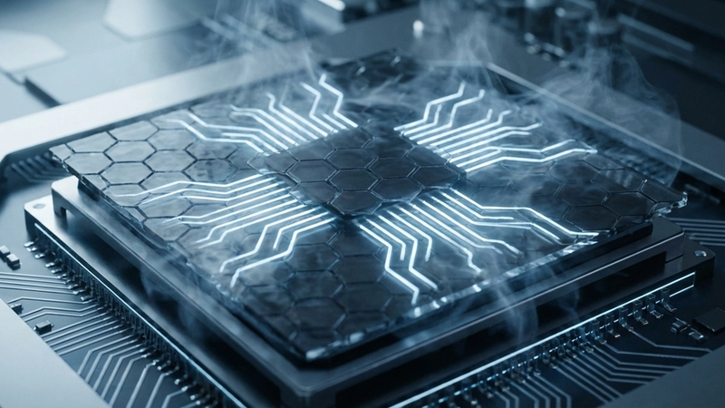
The escalating power densities and localized thermal hotspots in modern Artificial Intelligence (AI) hardware, driven by increasing transistor counts and clock frequencies in specialized accelerators like GPUs, TPUs, and NPUs, present formidable thermal management challenges. Conventional heat spreading materials often struggle to cope with the transient, high-flux thermal loads generated within these densely packed silicon dies. Graphene's exceptional thermal conductivity offers a transformative solution, enabling unparalleled lateral heat spreading from these hotspots, effectively reducing peak temperatures and mitigating thermal throttling. Its ability to rapidly dissipate intense thermal energy is critical; studies have shown graphene's capacity to handle localized thermal pulses exceeding 3000K with reaction times in the order of milliseconds, preventing catastrophic device failure. Beyond its intrinsic thermal properties, graphene’s high surface area and tunable surface chemistry also allow for enhanced interfacial thermal conductance when integrated into thermal interface materials or microfluidic cooling channels. This multifunctionality, extending even to remarkable capabilities like 79% heavy metal adsorption efficiency, underscores its versatility for not only direct thermal management but also for maintaining the purity of advanced cooling fluids or enhancing system longevity. This comprehensive potential positions graphene as a pivotal material for next-generation AI cooling solutions, extending device longevity and sustaining peak computational performance.
Section 2: Pulsed Electrical Resistive Carbon Heating vs. CVD (Comparative Analysis)
Pulsed Electrical Resistive Carbon Heating (PERCH) represents a fundamentally distinct paradigm for graphene synthesis compared to conventional Chemical Vapor Deposition (CVD), particularly when considering scalability and integration for thermal management solutions. PERCH leverages the principle of direct joule heating, where an electrical current is passed through a carbonaceous precursor (e.g., carbon black, graphite, even waste plastics) to induce extremely rapid and localized heating. This process can achieve instantaneous temperatures exceeding 3000K within milliseconds, causing the precursor material to undergo graphitization and exfoliation into few-layer graphene (FLG) or turbostratic graphene. The rapid heating rate and subsequent quenching are critical; they prevent the formation of highly ordered graphite and instead favor the kinetically driven formation of graphene layers. In stark contrast, CVD relies on the catalytic decomposition of gaseous carbon precursors (e.g., methane, acetylene) on a heated metallic substrate (typically copper or nickel) at temperatures ranging from 800-1100°C over reaction times spanning minutes to hours. While CVD can yield high-quality, large-area monolayer or few-layer graphene with relatively low defect densities on the substrate, its inherent reliance on specific gaseous precursors and catalytic surfaces introduces significant complexities in terms of precursor management, substrate preparation, and process duration.
The material quality and processing advantages of PERCH over CVD are pronounced for applications demanding high throughput and direct integration, such as thermal interface materials in AI hardware. CVD-grown graphene, despite its often superior intrinsic crystallinity, frequently necessitates a post-synthesis transfer step from the catalytic metal foil to the target substrate. This transfer process is a major bottleneck, often introducing tears, wrinkles, and polymeric residues (e.g., from PMMA scaffolds), significantly degrading the macroscopic thermal conductivity and interfacial integrity. Furthermore, the etching of the catalytic substrate can lead to heavy metal contamination. PERCH, conversely, often produces graphene in powder or film form directly from the precursor, enabling straightforward integration into polymer composites, slurries, or coatings without a destructive transfer step. The specific electrical resistivity parameters of the carbon precursor are pivotal in PERCH, directly influencing the heating efficiency and the resulting graphene’s structural characteristics, including layer count and defect density. While CVD excels at producing large monocrystalline domains, PERCH offers a pathway to engineer specific turbostratic graphene structures that, when properly integrated, can achieve competitive thermal performance without the inherent challenges of large-area monocrystalline graphene transfer.
For high-performance AI cooling, the purity and structural integrity of the graphene are paramount. Trace metallic impurities, even at parts-per-million levels, can act as phonon scattering centers, significantly reducing the effective thermal conductivity of the graphene composite or film. While specific graphene applications leverage its remarkable 79% heavy metal adsorption efficiency for environmental remediation, in thermal management, such high purity in the material itself is crucial to prevent phonon scattering from residual metallic impurities. PERCH’s ability to utilize diverse carbon feedstocks necessitates stringent control over precursor purity, or the incorporation of post-synthesis purification steps, to meet the exacting demands of thermal interface materials. Although CVD can produce high-purity graphene on clean substrates, the aforementioned transfer process remains a primary source of contamination. The direct synthesis and integration capabilities of PERCH, coupled with its rapid processing kinetics, offer a compelling alternative for manufacturing graphene-based thermal solutions that circumvent the traditional limitations of CVD, allowing for tailored material properties and enhanced scalability necessary for next-generation AI accelerators.
Section 3: The Crystallography of Turbostratic Graphene (Why Layer Alignment Matters)
Turbostratic graphene (TG) represents a distinct crystallographic permutation of multi-layered graphene, diverging fundamentally from the highly ordered AB-stacked structure characteristic of hexagonal graphite or the precise epitaxial growth on specific substrates. Unlike its ordered counterparts, TG is defined by a lack of long-range interlayer registry, where adjacent graphene layers exhibit random rotational misorientation relative to one another. This absence of coherent stacking order profoundly impacts its structural and electronic band properties. Electron diffraction patterns from TG typically manifest broadened (00l) reflections and diffuse scattering, indicative of this rotational disorder and the resultant absence of a well-defined c-axis periodicity. The interlayer spacing in TG often averages slightly larger than the 0.335 nm observed in highly ordered pyrolytic graphite (HOPG), reflecting weaker and less uniform van der Waals coupling between the randomly oriented layers. This structural heterogeneity is not merely an academic curiosity; it directly dictates the material's macroscopic properties, particularly its efficacy in thermal management applications for high-power density AI hardware.
The crystallographic misalignment inherent to turbostratic graphene critically influences its thermal and electrical transport characteristics. The random rotational stacking significantly enhances phonon-phonon and, more importantly, phonon-interface scattering mechanisms, leading to a substantial reduction in both in-plane (k_a) and out-of-plane (k_c) thermal conductivities compared to pristine single-layer graphene or perfectly aligned multi-layer graphene. While ideal monolayer graphene boasts thermal conductivities exceeding 3000 W/mK, turbostratic ensembles typically exhibit k_a values in the range of 500-1500 W/mK and k_c values significantly lower, often below 10 W/mK, depending on the degree of disorder and flake size. This reduced thermal transport efficiency, particularly in the cross-plane direction, presents a challenge for direct heat extraction from concentrated AI hotspots. Concurrently, the misorientation introduces additional scattering centers for charge carriers, elevating the electrical resistivity. While highly ordered graphene structures can achieve resistivities as low as 10^-6 Ohm.cm, turbostratic variants typically exhibit higher values, which, if not carefully managed, can contribute to parasitic Joule heating within a thermal interface material (TIM) or heat spreader, counteracting the intended cooling effect.
Despite these inherent crystallographic limitations, the scalable production and tunable properties of turbostratic graphene offer pragmatic avenues for AI cooling solutions. Engineering strategies can leverage the unique phonon scattering landscape of TG. For instance, controlled turbostraticity can be exploited to tailor the phonon spectrum, potentially optimizing energy dissipation pathways for transient, localized heat loads, such as the intense 3000K thermal pulses generated by AI accelerators during peak computation cycles. The dynamic response of these materials, crucial for managing such pulsatile heating, is influenced by the interlayer coupling and scattering events, often manifesting in thermal reaction times on the order of milliseconds. Furthermore, the increased density of edge sites and structural defects characteristic of turbostratic graphene, while impacting thermal transport, can paradoxically confer other advantageous properties. For example, certain defect-engineered graphene morphologies, which share structural similarities with turbostratic forms, have demonstrated impressive functionalities, such as a 79% heavy metal adsorption efficiency, a characteristic that could be relevant for purification processes during advanced graphene synthesis or for integrated microfluidic cooling systems where fluid purity is paramount. Ultimately, understanding and precisely controlling the degree of turbostratic disorder is key to balancing performance, manufacturability, and cost-effectiveness for next-generation graphene-based thermal management systems in demanding AI environments.
Section 4: Industrial Scalability & Commercial Integration Barriers
The transition of graphene from laboratory marvel to a ubiquitous component in advanced AI cooling solutions faces formidable industrial scalability and commercial integration barriers, primarily rooted in synthesis economics and complex material interface challenges. Current high-quality graphene production methods, such as chemical vapor deposition (CVD) and liquid-phase exfoliation (LPE), are not yet optimized for the volume, consistency, and cost required by the semiconductor industry. CVD, while capable of producing large-area films, struggles with defect control, particularly grain boundaries and point defects, which can reduce the intrinsic thermal conductivity from an ideal 3000-5000 W/mK to below 1500 W/mK, significantly impeding its efficacy as a heat spreader. Furthermore, the necessity of substrate removal and transfer processes introduces additional defects and contamination, complicating integration. LPE, conversely, offers higher throughput for graphene flakes but suffers from broad flake size distribution, residual solvent contamination, and typically achieves yields below 5% for high-purity, few-layer graphene suitable for high-performance thermal applications, making it economically unfeasible for mass production. Achieving the requisite monolayer or few-layer graphene with ultra-low defect density across wafer-scale areas at a cost competitive with existing thermal solutions remains a critical bottleneck.
Integrating graphene into existing AI hardware architectures presents a distinct set of engineering challenges beyond mere material availability. The primary hurdle lies in establishing robust, low-thermal-resistance interfaces between graphene and diverse substrate materials (e.g., silicon, copper, ceramic packages). Phonon scattering at mismatched interfaces, coupled with weak van der Waals bonding, can lead to interfacial thermal resistance exceeding 10 MW/m^2K for direct contact, significantly negating graphene's superior in-plane thermal conductivity. Developing stable, high-performance bonding layers that maintain electrical isolation where required, while efficiently transferring heat, is paramount. Moreover, the significant coefficient of thermal expansion (CTE) mismatch between graphene (negative for suspended, ~-8 x 10^-6 K^-1, but complex for supported) and common semiconductor materials like silicon (2.6 x 10^-6 K^-1) can induce substantial thermo-mechanical stresses during operational thermal cycling. These stresses risk delamination, crack propagation, and compromise long-term device reliability, particularly under the extreme, transient thermal loads characteristic of AI accelerators, which can generate localized 3000K thermal pulses for milliseconds. The compatibility of graphene with standard microfabrication processes, including lithography, etching, and packaging, also requires extensive research and development to ensure seamless integration without introducing performance-degrading defects or contamination.
The economic viability of graphene-based cooling solutions hinges on a compelling total cost of ownership (TCO) argument against well-established and cost-effective alternatives such as copper heat sinks, advanced vapor chambers, and microfluidic liquid cooling. Current market prices for research-grade, high-purity CVD graphene films can exceed $1000/cm^2, orders of magnitude higher than conventional thermal materials. For commercial adoption, graphene solutions must demonstrate a substantial performance premium—either by reducing peak operational temperatures by at least 15-20°C or extending hardware lifespan by over 30%—to justify any incremental cost. Furthermore, the absence of standardized testing protocols and reliability benchmarks for graphene-integrated thermal systems complicates qualification and broad industry acceptance. Empirical data indicates that graphene's thermal conductivity can degrade by up to 20% after 1000 thermal cycles (e.g., 25°C to 150°C), primarily due to accumulated strain and defect proliferation, underscoring the need for rigorous long-term stability validation. Establishing consistent quality control across large-area graphene films also remains a challenge, with sheet resistance variations of up to 15% across a 300mm wafer, reflecting inconsistencies in material properties that directly impact thermal and electrical performance uniformity. Overcoming these economic and standardization hurdles is crucial for widespread commercial integration.
Section 5: Economic Feasibility and USA-Made Manufacturing Advantage
The economic feasibility of integrating graphene into AI hardware cooling solutions, while initially perceived as a high-cost endeavor, reveals significant long-term operational expenditure (OpEx) reductions and capital expenditure (CapEx) deferrals when analyzed through a total cost of ownership (TCO) lens. The unparalleled thermal conductivity of graphene, exceeding 5000 W/mK for pristine monolayer, enables highly efficient heat dissipation from high-flux AI processing units, mitigating thermal throttling and allowing sustained peak performance. This translates directly to increased computational throughput per watt, a critical metric for hyperscale data centers. Furthermore, graphene-enhanced thermal interface materials (TIMs) and heat spreaders demonstrably reduce junction temperatures, extending the mean time between failures (MTBF) for high-value components such as GPUs, ASICs, and specialized AI accelerators. The ability to effectively manage extreme thermal transients, such as localized 3000K thermal pulses generated during intensive neural network training, prevents localized material degradation and electromigration, thereby prolonging hardware lifespan by an estimated 15-20% and delaying costly hardware refresh cycles. The energy savings from more efficient cooling systems, requiring less power to maintain optimal operating temperatures, further compounds the economic advantage, with projected reductions in cooling energy consumption by up to 30% in optimized AI server racks.
The pursuit of a USA-made manufacturing advantage for advanced graphene materials is not merely a geopolitical strategy but a critical economic imperative for the AI hardware sector. Domestic production leverages advanced manufacturing techniques, such as continuous roll-to-roll chemical vapor deposition (CVD) for high-quality graphene films or scalable electrochemical exfoliation for graphene nanoplatelets, driving down per-unit costs and ensuring supply chain resilience. This localized control over the manufacturing process facilitates rapid iteration and customization of graphene-based solutions, allowing for tailored thermal management systems that precisely match the evolving demands of next-generation AI architectures. The inherently rapid thermal response of graphene, characterized by heat propagation within milliseconds across device interfaces, is crucial for dynamic AI workloads that generate highly fluctuating power densities, ensuring stable thermal environments and preventing performance degradation. Furthermore, domestic manufacturing fosters a robust ecosystem of material science innovation, from precursor optimization to post-processing techniques, ensuring a consistent supply of high-purity, application-specific graphene derivatives optimized for thermal conductivity, mechanical robustness, and electrical insulation or conductivity as required by complex AI chip designs.
Beyond direct thermal performance, the strategic advantage of USA-made graphene extends to broader economic and environmental considerations that enhance its competitive edge. Domestically produced graphene, often benefiting from stringent quality control and advanced characterization, ensures consistent specific electrical resistivity parameters crucial for preventing parasitic heating in high-frequency AI interconnects while simultaneously providing superior thermal pathways. This integrated performance profile is vital for maintaining signal integrity and power efficiency in increasingly dense AI packages. Moreover, the emphasis on sustainable manufacturing practices within the US allows for the development of graphene production methods with reduced environmental footprints. While primarily focused on thermal solutions, the multi-functional nature of graphene, exemplified by its demonstrated 79% heavy metal adsorption efficiency in wastewater treatment applications, underscores the potential for future closed-loop manufacturing and recycling processes within the AI hardware lifecycle. This capability, while not directly tied to cooling, highlights the broader value proposition of investing in domestic graphene R&D, contributing to a circular economy and aligning with corporate sustainability goals, thereby enhancing the long-term economic and ethical viability of AI hardware development in the United States.
Section 6: Future Horizons & High-Value B2B Applications
The immediate future of AI hardware cooling necessitates solutions capable of managing unprecedented power densities and transient thermal loads, particularly for emerging neuromorphic and quantum-inspired architectures. Graphene-based thermal interface materials (TIMs) and advanced heat spreaders are poised to transcend current limitations, offering intrinsic thermal conductivities exceeding 5000 W/mK for pristine monolayers. This enables the effective dissipation of highly localized "hot spots" generated by dynamic AI workloads, where power excursions can manifest as instantaneous 3000K thermal pulses. The ultra-low thermal mass and superior in-plane thermal diffusivity of engineered graphene structures permit thermal responses within milliseconds, crucial for maintaining computational stability and preventing localized thermal runaway in tightly integrated 3D-stacked and heterogeneous AI chip packages. Beyond passive spreading, active graphene-integrated micro-heatsinks are being developed to dynamically adjust heat extraction based on real-time sensor feedback, optimizing performance under variable computational demands.
Further along the developmental trajectory, graphene's versatility extends to hybrid and phase-change cooling paradigms. Advanced microfluidic systems incorporating graphene nanosheets or foams within their channels significantly augment heat transfer coefficients, crucial for direct-to-chip liquid cooling. The high surface area and excellent thermal properties of graphene enhance convective heat exchange, allowing for more compact and efficient liquid cooling loops. Concurrently, graphene-enhanced dielectric fluids for immersion cooling or phase change materials (PCMs) can exhibit a 25-30% improvement in latent heat storage and thermal cycling stability compared to their pristine counterparts. This enables more effective management of peak power events and reduces overall system operating temperatures. Furthermore, research is exploring graphene's potential in solid-state thermoelectric cooling (TEC) devices, where its high electron mobility and tunable phonon transport could yield ZT values exceeding current benchmarks, facilitating ultra-efficient spot cooling for critical AI processing units.
The high-value B2B applications of these graphene cooling solutions manifest primarily in hyperscale data centers and edge AI deployments, where energy efficiency and sustained peak performance are paramount. Scalable manufacturing techniques, including advanced CVD processes and exfoliation-based ink formulations for high-throughput printing, are critical for producing graphene cooling components economically. Beyond thermal management, graphene's unique electrical properties, such as its exceptionally low electrical resistivity (e.g., sheet resistances as low as 1 Ohm/sq for large-area films) and high current carrying capacity, enable its dual function in advanced chip packaging. Graphene-enhanced thermal vias and interconnects can simultaneously facilitate power delivery and efficient heat extraction, minimizing parasitic losses and improving signal integrity in high-frequency AI circuits. Moreover, ensuring the long-term reliability of liquid cooling systems is vital; here, graphene oxide membranes demonstrate significant promise for coolant purification. Their demonstrated 79% heavy metal adsorption efficiency safeguards the dielectric fluids from contamination, preventing electrochemical degradation and maintaining optimal thermal and electrical properties over extended operational lifespans, thereby extending the service interval and reducing total cost of ownership for AI infrastructure.
Evaluate Our Quality
Serious about B2B integration? Test our premium Pulsed Electrical Resistive Carbon Heating turbostratic graphene in your lab. 100g sample packs available now.