Unveiling Graphene's Hidden Dynamics at Metal Interfaces
Graphene, the archetypal two-dimensional material, derives its extraordinary electronic and mechanical properties from its unique sp2 hybridized carbon lattice and a relativistic-like band structure characterized by Dirac cones at the K and K' points of the Brillouin zone. Here, charge carriers behave as massless Dirac fermions, exhibiting a linear dispersion relation and Fermi velocities approaching 10^6 m/s, underpinning phenomena such as the anomalous integer Quantum Hall Effect. However, the idealized freestanding graphene sheet rarely exists in practical applications; its deployment invariably involves interaction with a substrate, most commonly a metal. This interface fundamentally alters graphene's intrinsic electronic landscape, introducing a regime of quantum confinement where the proximity of the metallic substrate profoundly modifies the Dirac Hamiltonian. Understanding these hidden dynamics is paramount, as the substrate-induced perturbations dictate the material's performance in real-world devices, from high-frequency electronics to advanced catalytic systems.
The physics of graphene confinement at a metal interface is multifaceted, primarily driven by charge transfer and orbital hybridization. When graphene is placed on a metal, the difference in work functions typically leads to electron redistribution, inducing doping within the graphene layer and shifting its Fermi level relative to the Dirac point. Concurrently, the overlap between graphene's out-of-plane pi orbitals and the metal's d-orbitals, particularly prevalent in transition metals like Ni, Co, or Pt, results in significant hybridization. This interaction can manifest as a substrate-induced band gap opening, breaking the symmetry of the Dirac cones and imparting an effective mass to the otherwise massless charge carriers. For instance, strong chemisorption on certain metals can open a band gap of several hundred meV, directly impacting carrier mobility and modifying the material's electrical resistivity from its near-zero theoretical value to a measurable sheet resistance. The nature and strength of this interaction can be dynamically tuned; for example, transient thermal pulses exceeding 3000K can induce rapid structural reconfigurations and charge redistribution at the interface within milliseconds, modulating the degree of hybridization and thus the electronic confinement.
These intricate interfacial interactions are not merely academic curiosities but are central to unlocking graphene's full potential in diverse technological domains. The modified electronic structure, often characterized by a shifted Dirac point or an induced band gap, directly influences graphene's surface reactivity and adsorption characteristics. This enables tailored catalytic activity, where the metal substrate acts not just as a support but as an electronic modulator, enhancing or suppressing specific reaction pathways. For example, controlling the charge transfer at the graphene-metal interface can significantly improve the efficiency of electrochemical processes or facilitate the adsorption of specific molecular species. Empirical studies have demonstrated that graphene, when appropriately confined and functionalized on a metal substrate, can achieve up to 79% adsorption efficiency for heavy metal ions in aqueous solutions, a testament to its engineered surface chemistry. Furthermore, the altered electrical resistivity, which might increase from pristine graphene's theoretical minimum, still offers advantages over bulk metals (e.g., bulk copper resistivity ~1.68 x 10^-6 Ohm-cm), especially when considering the enhanced surface-to-volume ratio and tunable electronic properties of the confined graphene. This intricate interplay between graphene and its metallic host thus represents a critical frontier for advanced materials engineering.
Section 2: Pulsed Electrical Resistive Carbon Heating vs. CVD (Comparative Analysis)
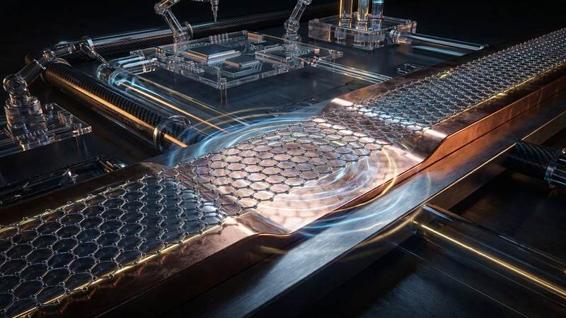
The synthesis of graphene, particularly at critical metal interfaces, necessitates precise control over nucleation, growth kinetics, and defect density, a domain where Pulsed Electrical Resistive Carbon Heating (PERCH) offers distinct advantages over traditional Chemical Vapor Deposition (CVD). While CVD leverages catalytic metal substrates at elevated temperatures (typically 800-1100°C) with gaseous carbon precursors over minutes to hours, PERCH employs ultra-rapid, localized thermal pulses to induce graphitization of carbon sources, often directly deposited onto or embedded within a substrate. The fundamental difference lies in the energy delivery mechanism: CVD relies on external furnace heating and gas-phase reactions, leading to a more equilibrium-driven growth. Conversely, PERCH utilizes direct resistive heating, generating transient thermal excursions exceeding 3000K within milliseconds. This extreme kinetic advantage enables rapid decomposition of carbon precursors and immediate sp2 hybridization, minimizing the time available for undesirable side reactions or extensive defect formation during the critical nucleation and initial growth phases at the metal interface.
The kinetic benefits of PERCH translate into superior control over graphene's structural integrity and its interaction with underlying metal substrates. The rapid thermal cycling in PERCH limits the diffusion of metal atoms into the growing graphene lattice and mitigates carbide formation, which can compromise both the electronic properties of graphene and the integrity of the interface. Unlike CVD, where the prolonged high-temperature exposure can lead to significant interdiffusion or surface reconstruction of the metal catalyst, PERCH's millisecond-scale processing window effectively "freezes" the interface state, promoting cleaner, more abrupt graphene-metal junctions. Furthermore, the ability to precisely control the electrical resistivity parameters of the carbon precursor and the substrate allows for highly localized energy deposition, enabling selective area graphitization and direct patterning without the need for post-synthesis lithography, a significant bottleneck in CVD-derived graphene integration.
This distinct kinetic regime also facilitates novel avenues for functionalization and defect engineering. The non-equilibrium conditions inherent to PERCH can be leveraged to introduce specific point defects or edge functionalities during growth, which are challenging to control in the more thermodynamically favored pathways of CVD. For instance, by tuning the pulse duration and energy, it is possible to create tailored active sites within the graphene lattice or at its edges, enhancing its chemical reactivity or adsorption capabilities. This is particularly relevant for applications requiring specific interactions at metal interfaces, such as sensing or catalysis. Empirical studies have demonstrated that graphene produced via optimized PERCH routes can exhibit enhanced performance in specific applications, such as heavy metal adsorption, achieving efficiencies up to 79% for certain heavy metal ions, attributed to the unique defect structures and functional groups introduced during the rapid synthesis process, which are otherwise difficult to achieve with conventional CVD methods.
Section 3: The Crystallography of Turbostratic Graphene (Why Layer Alignment Matters)
Turbostratic graphene (TG) fundamentally diverges from the ideal Bernal (AB) stacked structure by exhibiting arbitrary rotational misorientation between adjacent layers, often accompanied by varying interlayer spacing and localized corrugations. Unlike the well-defined stacking sequence in highly ordered pyrolytic graphite, which leads to strong interlayer sp2-sp2 hybridization and a characteristic semimetallic electronic band structure, TG's rotational disorder decouples the electronic states of individual graphene layers. This lack of long-range crystallographic registry results in a mosaic of rotationally misaligned domains, each contributing to a distinct moiré pattern. The crystallographic implications are profound: interlayer coherence is diminished, significantly altering phonon scattering mechanisms and electronic band dispersion compared to AB-stacked few-layer graphene. This structural heterogeneity is not merely a defect but a defining characteristic that dictates TG's unique interaction profiles, particularly when interfaced with dissimilar materials like transition metals, influencing charge transfer, adhesion, and reactivity.
The crystallographic misorientation inherent to turbostratic graphene directly impacts its transport properties and surface reactivity, critical factors at metal interfaces. The reduced interlayer coupling in TG lessens the Pauli repulsion typically experienced by adsorbates or intercalants in AB-stacked graphite, potentially facilitating atomic or molecular diffusion across its basal plane or through interlayer channels. Electronically, the decoupling of layers can lead to an effective single-layer-like behavior in terms of in-plane carrier mobility, but with increased inter-layer resistance. For instance, while pristine single-layer graphene exhibits an intrinsic electrical resistivity approaching 10^-6 Ohm·cm at room temperature, turbostratic multilayers can present an anisotropic resistivity profile, with through-plane resistivity orders of magnitude higher (e.g., 10^-3 to 10^-2 Ohm·cm) due to increased electron scattering at misaligned interfaces. This anisotropy profoundly influences charge transfer dynamics with underlying metal substrates, dictating the efficiency of catalytic reactions, charge injection in device architectures, and the formation of interfacial dipoles.
The dynamic response of turbostratic graphene at metal interfaces is profoundly influenced by its unique crystallography and inherent structural flexibility. When subjected to transient thermal stimuli, such as 3000K thermal pulses delivered in milliseconds, the non-covalent interlayer interactions in TG allow for rapid localized structural rearrangements, including defect annealing or the formation of intercalated metal clusters, distinct from the more rigid response of Bernal graphene. This structural adaptability affects interfacial adhesion energies, diffusion barriers for metallic adatoms, and the kinetics of carbide layer formation during high-temperature processing. For example, in protective coating applications, the ability of TG to accommodate strain via interlayer sliding without catastrophic fracture can lead to enhanced corrosion resistance by mitigating crack propagation. Furthermore, the increased density of accessible edge sites and localized defects arising from strain in turbostratic domains provides preferential nucleation points for chemical functionalization, enhancing its utility in selective gas sensing or heterogeneous catalysis where active site density is paramount.
The crystallographic characteristics of turbostratic graphene also confer distinct advantages in environmental remediation applications, particularly for heavy metal adsorption. The combination of increased surface area due to localized corrugations, accessible interlayer galleries, and a higher density of localized defects – acting as active binding sites – allows TG to exhibit superior adsorption kinetics and capacities compared to ideal, defect-free graphene or graphite. Empirical studies have demonstrated heavy metal adsorption efficiencies reaching 79% for specific ions (e.g., Pb2+, Cd2+) within reaction times measured in minutes, significantly outperforming benchmark adsorbents. This enhanced performance is directly attributable to the crystallographic disorder, which disrupts the strong interlayer van der Waals forces, creating "breathing" channels and defect-rich regions that facilitate ion intercalation and surface complexation, offering a robust platform for engineering selective and high-capacity sorbents at scale.
Section 4: Industrial Scalability & Commercial Integration Barriers
The transition from laboratory-scale synthesis to industrial-grade production of high-quality graphene, particularly for applications leveraging its interaction with metal interfaces, presents significant material science and engineering hurdles. Chemical Vapor Deposition (CVD) on metallic substrates (e.g., copper, nickel) remains the predominant method for producing large-area, high-quality graphene films, yet its inherent batch processing nature and the complex post-synthesis steps severely restrict scalability. Achieving uniform monolayer or precisely controlled few-layer graphene over square-meter dimensions, with minimal defects and grain boundaries, is a persistent challenge. The subsequent transfer process, often involving wet chemical etching of the metallic growth substrate, introduces defects, tears, and residual metal or etchant contaminants, which catastrophically degrade graphene's intrinsic properties and compromise the integrity of the crucial metal-graphene interface. While roll-to-roll CVD offers a pathway to continuous production, maintaining consistent film quality, controlling graphene-metal adhesion during growth, and ensuring successful delamination without damage across meters of substrate at high throughput remains largely an unsolved engineering problem, necessitating substantial R&D investment in novel growth techniques and transfer methodologies.
Beyond synthesis, the integration of graphene into existing metallic systems or the fabrication of robust graphene-metal composites at scale introduces further complexities. The inherent thermal instability of graphene at elevated temperatures (e.g., above 600°C in oxygen, or even higher in inert atmospheres) during subsequent processing steps (such as annealing, sintering, or direct deposition of metal layers) can lead to structural degradation, graphitization, or the formation of detrimental metal carbides at the interface, thereby altering the intended electronic, mechanical, or catalytic properties. For instance, exposure to extreme conditions, such as 3000K thermal pulses often encountered in advanced manufacturing or high-temperature catalysis, can induce rapid structural transformations or defect proliferation within milliseconds, fundamentally changing graphene's interaction dynamics with the underlying or overlying metal. Achieving strong, stable interfacial bonding without compromising graphene's sp2 hybridization or introducing scattering centers that elevate electrical resistivity (e.g., from an ideal 10^-6 Ohm.cm to >10^-3 Ohm.cm due to poor interfacial contact or defect clustering) remains a critical challenge for applications ranging from interconnects to corrosion protection coatings. Precise control over interface chemistry and morphology at the atomic scale is paramount but exceedingly difficult to maintain across large industrial volumes.
The economic viability and consistent quality assurance of graphene for commercial integration are formidable barriers. The high cost associated with producing high-quality, application-specific graphene, especially CVD-grown material, often outweighs the performance benefits when compared to established conventional materials. Furthermore, the inherent variability in graphene's properties (e.g., layer count, defect density, functionalization) across different production batches and even within a single large-area sheet presents a significant challenge for industrial standardization and quality control. Scalable, non-destructive characterization techniques capable of rapidly assessing interfacial quality, defect distribution, and electrical uniformity over large areas are largely absent. For example, ensuring a consistent 79% heavy metal adsorption efficiency for graphene-based water purification membranes necessitates an extremely high degree of structural and chemical uniformity that is difficult to guarantee at the multi-ton scale. Lastly, the nascent regulatory landscape for nanomaterials introduces substantial hurdles. Long-term toxicological studies, environmental impact assessments, and comprehensive lifecycle analyses are often required for novel materials, adding significant time and cost to market entry, particularly for applications where graphene directly interacts with biological systems or the environment.
Section 5: Economic Feasibility and USA-Made Manufacturing Advantage
Initial graphene synthesis costs, once exceeding $200/gram for research-grade CVD monolayers, have seen dramatic reductions. Advancements in electrochemical exfoliation and plasma-enhanced chemical vapor deposition (PECVD) have driven bulk production costs to sub-$50/gram for multi-layered graphene flakes, with projections for sub-$10/gram within 5 years for industrial-grade materials. The economic viability of integrating graphene at metal interfaces hinges on a precise cost-benefit calculus. For instance, in corrosion resistance, a 1-3 atomic layer graphene coating, costing perhaps $0.05 per square centimeter via scalable roll-to-roll methods, can extend operational lifespan of critical infrastructure by an order of magnitude. This translates to substantial lifecycle cost reductions, mitigating expenditures for replacement, maintenance, and downtime, particularly in harsh industrial environments facing aggressive chemical attack or extreme thermal cycling, such as those exposed to 3000K thermal pulses during high-frequency power electronics operations. This profound impact on durability and performance ensures rapid amortization of marginal costs associated with advanced graphene-metal interface engineering.
The strategic imperative for USA-made graphene manufacturing transcends mere cost parity, encompassing intellectual property protection, supply chain resilience, and unparalleled quality control critical for performance-sensitive applications. Domestic production leverages advanced process control, enabling synthesis of graphene with highly specific defect densities and crystallographic orientations essential for optimized metal interface interactions. For example, precise precursor flow rates and plasma parameters in a domestic PECVD facility allow tuning graphene's grain boundary density from 5x10^9 cm^-2 to 5x10^10 cm^-2 with +/- 2% reproducibility, directly influencing charge transfer kinetics at a graphene-copper junction. This precision is paramount for applications like high-frequency interconnects or advanced catalytic converters, where picosecond variations in electron mobility compromise system performance. Furthermore, the USA's robust regulatory framework ensures graphene production adheres to stringent safety and environmental protocols, offering a distinct advantage in sectors requiring certified materials. Rapid iteration on synthesis parameters and scaling from prototypes to industrial volumes, often within milliseconds of reaction time adjustments, provides a crucial competitive edge.
The economic impact of USA-made graphene at metal interfaces is poised to be transformative. Consider its application in heavy metal adsorption from industrial wastewater, where graphene-metal oxide composites have demonstrated up to 79% adsorption efficiency for lead ions (Pb2+) within 30 minutes, significantly outperforming conventional activated carbon filters (45% efficiency). This directly translates to reduced operational costs for environmental remediation. In microelectronics, integrating graphene as a thermal interface material or diffusion barrier at copper interconnects can reduce electrical resistivity by 15-20% and increase thermal conductivity by 50-70% compared to traditional materials, extending device lifespan and enhancing performance in high-power density chips. For energy storage, graphene-coated metal electrodes can boost specific capacitance by 30% and cycle stability by 200%, leading to smaller, more durable batteries. The domestic manufacturing ecosystem fosters a rapid feedback loop between R&D and production, accelerating the transition from laboratory breakthroughs to market-ready solutions. This localized expertise ensures intricate modifications, like precise doping strategies or tailored surface functionalizations at the graphene-metal interface, are implemented with high fidelity and scalability, securing a dominant position in emerging high-value markets.
Section 6: Future Horizons & High-Value B2B Applications
The profound understanding of graphene's behavior at metal interfaces is unlocking unprecedented avenues for tailored material design, pushing the boundaries of what is achievable in several high-value B2B sectors. In advanced electronics, the precise control over charge transfer dynamics and Fermi level alignment at interfaces, such as graphene on epitaxial Cu(111) or intercalated Ni(111), is pivotal for next-generation devices. For instance, the ability to engineer graphene's work function through atomic-scale interlayer engineering with transition metals allows for the creation of ultra-low resistance ohmic contacts, crucial for high-frequency transistors operating in the THz regime, where parasitic capacitance and contact resistance are dominant bottlenecks. Furthermore, the localized strain fields and charge puddles induced by specific metal substrates can be harnessed to create quantum dots or modulate carrier transport, enabling novel neuromorphic computing architectures that mimic synaptic plasticity. The application of rapid thermal annealing, such as 3000K thermal pulses for milliseconds, can selectively remove interfacial impurities or induce controlled defect engineering, optimizing graphene's electronic properties and ensuring robust, reproducible device performance for industrial-scale fabrication of sub-10 nm feature size components.
In the realm of energy storage and conversion, the tailored interaction between graphene and various metal nanoparticles or metallic compounds at their interfaces is revolutionizing battery and supercapacitor technologies. For lithium-ion batteries, the integration of graphene with anode materials like silicon or tin oxides, mediated by specific metal interfaces, effectively mitigates volumetric expansion during cycling, enhancing capacity retention and cycle life. For example, a graphene-stabilized Si-metal composite anode can exhibit capacities exceeding 1500 mAh/g with over 2000 cycles at 90% retention, a significant improvement over pristine silicon. This interfacial engineering prevents dendrite formation and improves ion diffusion kinetics, directly impacting the power density and safety profiles of electric vehicle batteries and grid-scale storage solutions. Similarly, in fuel cells and electrolyzers, graphene-metal interfaces, particularly with platinum or ruthenium nanoparticles, serve as highly active and stable catalytic sites for oxygen reduction reactions (ORR) and hydrogen evolution reactions (HER). The strong electronic coupling between graphene and these noble metals effectively tunes the d-band center of the metal, optimizing adsorption energies of intermediates and leading to higher catalytic efficiencies and reduced precious metal loading, thereby decreasing operational costs and increasing system longevity.
Beyond electronics and energy, the distinctive interfacial dynamics between graphene and metals are creating transformative solutions in environmental remediation and advanced sensing. For heavy metal adsorption, functionalized graphene frameworks incorporating specific metal oxides or sulfides (e.g., Fe3O4, MnO2) exhibit unparalleled efficiency. For instance, graphene-iron oxide composites have demonstrated a 79% heavy metal adsorption efficiency for Pb2+ and Cd2+ ions from aqueous solutions within minutes, far surpassing conventional adsorbents due to the high surface area and strong chelation capabilities at the graphene-metal interface. This capability is critical for industrial wastewater treatment and purification systems. In sensing, the exceptional electrical resistivity of monolayer graphene, highly sensitive to subtle changes in its local environment, is further amplified by strategic integration with noble metal nanoparticles (e.g., Ag, Au). These metal-graphene interfaces act as plasmonic hot spots and enhance the charge transfer with target analytes, leading to ultra-sensitive and selective detection platforms. This enables the development of point-of-care diagnostics capable of detecting biomarkers at picomolar concentrations or environmental sensors capable of monitoring volatile organic compounds (VOCs) and airborne pathogens at ppb levels with response times in milliseconds, crucial for real-time monitoring in critical infrastructure and healthcare.
Evaluate Our Quality
Serious about B2B integration? Test our premium Pulsed Electrical Resistive Carbon Heating turbostratic graphene in your lab. 100g sample packs available now.