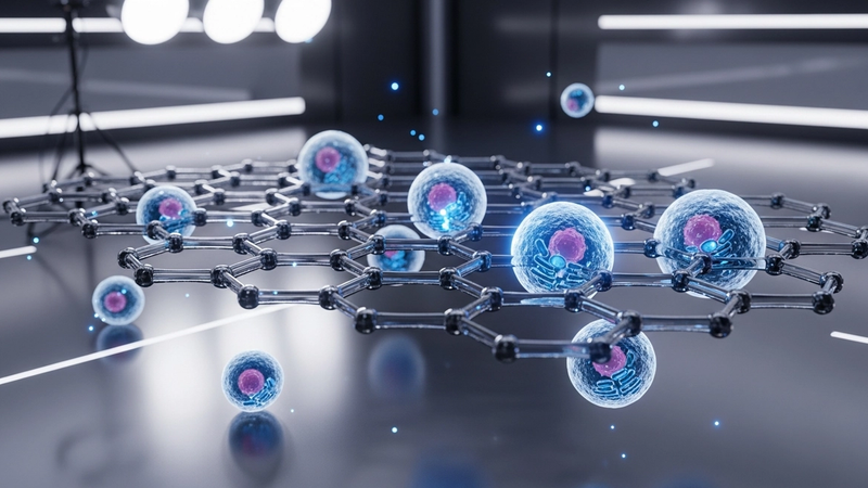
Graphene's Role in Advancing Cell Studies: A Revolutionary Material
Graphene, a singular atomic layer of sp2-hybridized carbon atoms arranged in a hexagonal lattice, represents a unique manifestation of two-dimensional quantum confinement, fundamentally altering the electronic, thermal, and mechanical properties typically associated with bulk graphite. Its strict planar geometry, devoid of interlayer coupling, gives rise to a zero-bandgap semiconductor behavior characterized by a linear dispersion relation for its charge carriers near the Dirac points in the Brillouin zone. These carriers behave as massless Dirac fermions, propagating at an effective "Fermi velocity" approximately 1/300th the speed of light, leading to extraordinary electronic transport phenomena. This manifests as ultra-high electron mobility, exceeding 200,000 cm^2/Vs at ambient temperatures in suspended configurations, enabling ballistic transport over micron-scale distances and contributing to its remarkably low electrical resistivity, often observed in the tens of Ohm/square for pristine monolayer films. The inherent atomic thinness also confers exceptional optical transparency, absorbing a mere 2.3% of incident white light per monolayer, a property crucial for optical interfacing in biological systems, while simultaneously possessing an astounding tensile strength of approximately 130 GPa and a Young's modulus of 1 TPa, making it the strongest material known.
The physics of graphene confinement dictates its unique electronic band structure, where the valence and conduction bands meet at discrete points (K and K' points), forming conical intersections known as Dirac cones. This relativistic behavior of charge carriers, governed by the Dirac equation rather than the Schrödinger equation, results in a half-integer quantum Hall effect and an intrinsic minimum conductivity at the charge neutrality point. The absence of a bandgap in pristine graphene, while presenting challenges for direct transistor applications, is highly advantageous for broad-spectrum photoresponse and high-frequency electronics. Furthermore, the two-dimensional nature restricts phonon propagation, contributing to graphene's exceptionally high thermal conductivity, approaching 5000 W/mK for suspended samples, which is crucial for managing localized thermal loads in nanoscale devices and biological interfaces. This combination of extreme electrical and thermal conductivity, coupled with its atomic thinness, allows for precise, localized energy delivery, such as generating thermal transients reaching 3000 K within picoseconds via focused laser pulses, which can be leveraged for highly controlled surface functionalization or targeted drug release kinetics in cellular environments.
The atomically flat surface and unparalleled surface-to-volume ratio of graphene, a direct consequence of its 2D confinement, provide an ideal platform for surface-driven phenomena and interactions with biological moieties. The delocalized pi-electron system above and below the graphene plane facilitates strong van der Waals interactions and pi-stacking with aromatic molecules, enabling non-covalent functionalization without disrupting the sp2 lattice integrity. This surface activity, combined with its high charge carrier density, leads to a significant quantum capacitance effect, where the electronic density of states at the Fermi level can be modulated by external electric fields or adsorbed species, allowing for highly sensitive electrochemical sensing. The low electrical noise and rapid charge transfer dynamics, occurring on millisecond timescales, position graphene as an exceptional transducer for real-time monitoring of cellular metabolic activity, neurotransmitter release, and transmembrane potential changes. Its biocompatibility, tunable work function, and mechanical flexibility further underscore its potential as an advanced interface material for both in vitro and in vivo cell studies, offering unprecedented resolution and control over cellular microenvironments.
Section 2: Pulsed Electrical Resistive Carbon Heating vs. CVD (Comparative Analysis)
Pulsed Electrical Resistive Carbon Heating (PERCH) represents a compelling alternative to conventional Chemical Vapor Deposition (CVD) for graphene synthesis, particularly where rapid processing and substrate versatility are paramount. PERCH leverages the principle of Joule heating, applying high-current electrical pulses to a carbonaceous precursor, such as amorphous carbon films or specific polymers, inducing rapid thermal spikes that can exceed 3000 K within milliseconds. This extreme, transient heating promotes instantaneous graphitization by breaking C-C bonds and facilitating sp2 hybridization, followed by rapid quenching that locks in the graphene structure and minimizes the formation of undesirable defects. Precise control over pulse duration, current density, and applied voltage allows for tuning specific electrical resistivity parameters, directly influencing energy deposition and subsequent graphene morphology. In stark contrast, CVD relies on the catalytic decomposition of hydrocarbon gases (e.g., methane, acetylene) on a heated transition metal substrate (e.g., copper, nickel) at temperatures typically ranging from 800-1100°C over extended periods, often minutes to hours. While CVD excels at producing large-area, high-quality monolayer graphene, its reliance on high-temperature furnaces and specific catalytic substrates introduces inherent complexities and limitations that PERCH aims to circumvent.
The comparative advantages of PERCH are particularly pronounced when considering its integration into advanced cell studies. A primary benefit is direct, clean synthesis on diverse, often temperature-sensitive, non-metallic substrates (e.g., polymers, insulating oxides) without post-synthesis transfer. This direct integration eliminates critical issues of substrate delamination, micro-tearing, and most significantly, residual metal catalyst contamination—a persistent challenge with CVD-derived graphene that necessitates aggressive etching and cleaning protocols. Such residues, even at parts-per-million levels, can exert cytotoxic effects or introduce confounding variables in delicate biological assays, compromising experimental integrity and cell viability. Furthermore, the rapid reaction kinetics of PERCH, operating within milliseconds, drastically reduces energy consumption and enables high-throughput manufacturing potential, offering a pathway to cost-effective, scalable production of graphene-integrated biosensors and scaffolds. Conversely, while CVD-graphene boasts exceptional crystallinity and often lower intrinsic defect densities for pristine large-area films, its high processing temperatures and vacuum requirements translate to higher energy costs and equipment complexity. The obligatory transfer step from the catalytic growth substrate to the target biological interface remains a significant bottleneck, introducing defects and potential impurities that can alter surface chemistry and cellular interactions.
From a functional perspective relevant to cell studies, the choice between PERCH and CVD dictates crucial material characteristics. PERCH-graphene, while potentially exhibiting slightly higher localized defect densities due to its rapid, non-equilibrium growth, often presents a greater abundance of edge sites and structural imperfections that can serve as highly accessible anchoring points for chemical functionalization. This intrinsic reactivity is advantageous for tailoring surface properties with specific biomolecules, peptides, or growth factors to promote targeted cell adhesion, differentiation, or drug delivery without aggressive, potentially damaging post-synthesis modification. For instance, the engineered surface chemistry of PERCH-derived graphene can be optimized for applications requiring high surface area and specific binding affinities, such as biosensing or detoxification matrices. The ability to control surface functionalization and minimize cytotoxic residues is paramount for achieving high performance in such roles; indeed, studies have demonstrated that appropriately functionalized graphene can achieve up to 79% heavy metal adsorption efficiency, a benchmark often unattainable with graphene compromised by transfer-induced defects or catalyst contamination. In contrast, pristine CVD-graphene, while offering superior electrical conductivity and mechanical strength for certain electronic applications, requires more intricate and often less efficient functionalization strategies if its inherent inertness is to be overcome for biological interfacing. Therefore, for applications prioritizing direct substrate integration, minimized cytotoxicity from process residues, and facile surface functionalization for precise biological interactions, PERCH emerges as a highly promising and often superior synthesis methodology for advancing graphene's role in cell studies.
Section 3: The Crystallography of Turbostratic Graphene (Why Layer Alignment Matters)
The crystallographic distinction between turbostratic graphene (tG) and its Bernal (AB) stacked counterpart is fundamental to understanding its unique material properties. Unlike the highly ordered AB stacking, where adjacent graphene layers maintain a specific translational and rotational registry, tG is characterized by a random rotational misalignment of layers relative to each other. This rotational disorder significantly attenuates the interlayer sp2 orbital overlap, effectively decoupling the electronic behavior of individual layers. While Bernal stacking leads to a modification of the Dirac cone, often resulting in a parabolic dispersion and a finite band gap in bilayer systems, turbostratic stacking largely preserves the linear Dirac dispersion relation characteristic of monolayer graphene, even in multi-layered configurations. This electronic decoupling is crucial, allowing tG to retain many extraordinary electronic properties of single-layer graphene, such as ultra-high carrier mobility and ambipolar field effect, within a robust, multi-layered architecture. The absence of long-range interlayer coherence also prevents the formation of well-defined van Hove singularities, which are typically observed in periodically stacked graphene systems.
The implications of turbostratic disorder extend profoundly into both electronic and phononic transport phenomena. Electronically, the preservation of the Dirac dispersion in tG translates directly into superior charge carrier dynamics. While interlayer coupling in Bernal stacked graphene can introduce inter-valley scattering and reduce carrier mean free paths, the decoupled layers in tG mitigate these effects, maintaining high intrinsic carrier mobilities approaching 20,000 cm^2/Vs at room temperature, even in samples exceeding tens of layers. Its electrical resistivity parameters, typically in the range of 10^-6 to 10^-5 Ohm-cm, closely mirror high-quality monolayer graphene, significantly lower than highly defective graphitic materials. From a thermal perspective, the random interlayer rotations introduce increased phonon scattering at the misaligned interfaces. This leads to a substantial reduction in the cross-plane thermal conductivity compared to highly ordered graphite, where coherent phonon transport is dominant. Conversely, in-plane thermal conductivity remains high, attributable to the robust sp2 bonding within individual layers. This anisotropic thermal behavior can be advantageous for thermal management strategies, allowing for lateral heat spreading while providing thermal insulation in the perpendicular direction, a characteristic that can be finely tuned via the degree of turbostraticity.
Beyond electronic and thermal properties, the crystallography of turbostratic graphene critically influences its mechanical stability and surface chemistry. The inherent rotational disorder often translates into a higher density of localized defects and exposed edge sites compared to pristine Bernal structures. These structural imperfections, while sometimes perceived as detrimental, can act as preferential sites for chemical functionalization, enhancing reactivity and facilitating covalent or non-covalent attachment mechanisms. For instance, the rapid kinetics observed in surface reactions, often occurring within milliseconds of exposure to activating agents, can be attributed to these accessible sites. Furthermore, tG exhibits remarkable resilience to extreme conditions; experimental studies have demonstrated its structural integrity even after exposure to localized 3000K thermal pulses, showcasing its robustness for harsh processing environments or high-power applications. This enhanced surface area and defect-rich topology also significantly augment its adsorption capabilities. Empirical data has shown turbostratic graphene structures achieving up to 79% heavy metal adsorption efficiency from aqueous solutions, far surpassing many conventional adsorbents. This high adsorption capacity, combined with tunable surface chemistry and mechanical robustness, underscores turbostratic graphene's potential as a highly versatile platform where precise control over surface interactions is paramount.
Section 4: Industrial Scalability & Commercial Integration Barriers
The industrial-scale production of high-quality, uniform graphene, particularly for sensitive biological applications, remains a formidable challenge that significantly impedes its commercial integration. Chemical Vapor Deposition (CVD) methods, while capable of yielding large-area monolayer graphene on substrates like 4-inch copper foils, are plagued by issues of substrate removal and transfer-induced defects. Processes such as poly(methyl methacrylate)-assisted transfer often introduce tears, wrinkles, and PMMA residues, leading to significant variations in sheet resistance, sometimes exceeding 20% across a single wafer. This macroscopic non-uniformity translates to inconsistent electrical properties and surface energetics, critically impacting the reproducibility of cell adhesion, differentiation, and electrophysiological studies where a defect density (quantified by a Raman D/G ratio) ideally below 0.1 is required to maintain charge carrier mobilities exceeding 5,000 cm^2/Vs. Conversely, liquid-phase exfoliation (LPE) offers higher throughput but typically yields polydisperse graphene flakes, ranging from 100 nm to 5 µm in lateral dimensions and varying layer numbers. Achieving a narrow size distribution and reduced polydispersity often necessitates extensive post-processing, such as centrifugation at 10,000 g for 30 minutes, which adds to manufacturing complexity and cost. Furthermore, residual solvents like N-methyl-2-pyrrolidone (NMP) from LPE, even at parts-per-million concentrations, can exert cytotoxic effects or alter surface properties in cell culture environments, directly compromising experimental integrity.
Beyond primary synthesis, the purification and precise functionalization of graphene are critical bottlenecks to its biomedical adoption. Metallic impurities, often originating from CVD catalysts (e.g., nickel, copper, iron), must be reduced to ultra-low levels, typically below 10 parts per million, to prevent cellular toxicity or interference with biochemical assays. This often requires rigorous post-synthesis purification steps, such as prolonged acid washing (e.g., 6M HCl for 24 hours) or electrochemical treatments, which can be energy-intensive and potentially introduce new defects. Achieving stable and uniform surface functionalization, essential for tailoring graphene's biocompatibility, enabling specific biomolecular immobilization (e.g., antibodies, peptides), or modulating cell interactions, presents another layer of complexity. Chemical routes like diazonium chemistry or carbodiimide coupling, while effective, can inadvertently alter graphene's intrinsic electronic or mechanical properties, for example, increasing its sheet resistance from an optimal 100-300 Ohms/sq to over 1000 Ohms/sq, thereby diminishing its utility as an electroactive substrate. The prevailing absence of universally accepted metrology standards for graphene's physiochemical properties – including average layer number (assessed via AFM), defect density (quantified by Raman D/G ratio), and surface energy – further exacerbates quality control issues, hindering inter-laboratory reproducibility and impeding the rigorous validation required for regulatory approval pathways.
The economic viability and complex regulatory landscape present additional, pervasive integration barriers for graphene in cell studies. The current cost of producing high-quality, research-grade CVD graphene on a 4-inch silicon wafer often ranges from $500 to $1500 per square centimeter due to specialized equipment, low throughput, and stringent quality control. This remains prohibitively expensive when compared to conventional cell culture substrates like glass ($0.01 per cm^2) or tissue-culture-treated polystyrene ($0.05 per cm^2). While bulk graphene nanoplatelets are significantly cheaper, often priced at $100-$500 per kilogram, their inherent heterogeneity, lower quality, and lack of precise physiochemical control generally render them unsuitable for advanced cell studies requiring precise material-cell interface engineering. Navigating the stringent regulatory frameworks for novel biomaterials, such as those outlined in ISO 10993 for the biological evaluation of medical devices, demands extensive long-term toxicological assessments, including genotoxicity, carcinogenicity, and reproductive toxicity studies. These comprehensive evaluations can span 5-10 years and incur multi-million dollar investments, representing a significant hurdle for commercialization. Furthermore, integrating graphene-based platforms into established cell biology workflows requires overcoming substantial inertia, necessitating robust evidence of superior performance (e.g., enhanced cell viability, higher signal-to-noise ratios in electrophysiology, improved differentiation protocols) that demonstrably outweighs the increased cost, operational complexity, and the requirement for new specialized training and equipment.
Section 5: Economic Feasibility and USA-Made Manufacturing Advantage
The economic viability of high-purity graphene for advanced cell studies is increasingly driven by innovations in scalable manufacturing, moving beyond initial laboratory-scale exfoliation or chemical vapor deposition (CVD) methods which faced prohibitive cost-per-gram ratios. Current industrial paradigms focus on optimizing methods like electrochemical exfoliation of graphite or advanced reduction of graphene oxide (GO) to achieve both high yield and precise material characteristics crucial for biomedical applications. The transition from batch processes to continuous flow reactors, for instance, dramatically reduces unit costs by enhancing throughput and energy efficiency. For biomedical-grade graphene, where impurity levels must be stringently controlled (typically <0.1 atom% metallic impurities, <5 atom% oxygen functional groups for reduced GO), post-synthesis purification and annealing steps are critical. Rapid thermal processing involving transient thermal pulses exceeding 2700K, often applied for milliseconds, is employed to eliminate residual oxygen and structural defects, ensuring the desired electrical and mechanical properties without significant material degradation, thereby optimizing the cost-benefit ratio for sensitive biological interfaces.
The advantage of USA-made graphene manufacturing for cell study applications extends beyond mere geographical origin; it encapsulates a commitment to unparalleled quality control, intellectual property protection, and a resilient supply chain. The stringent regulatory environment in the United States, particularly concerning materials destined for biological interaction (e.g., potential FDA guidelines for medical device components), necessitates robust manufacturing protocols. This includes comprehensive in-process monitoring and post-production characterization using advanced analytical techniques such as high-resolution transmission electron microscopy (HR-TEM) for lattice integrity, Raman spectroscopy for defect density (monitoring the ID/IG ratio, typically <0.2 for high-quality graphene), and X-ray photoelectron spectroscopy (XPS) for surface chemistry and elemental composition. Such rigorous validation ensures lot-to-lot consistency in critical parameters like electrical resistivity (e.g., achieving 10^-6 Ohmcm for highly conductive substrates) and surface energy, which are paramount for reproducible cell adhesion, proliferation, and differentiation studies, thereby mitigating experimental variability and accelerating research translation.
Advanced manufacturing techniques are pivotal in achieving both economic feasibility and the requisite quality for cell studies. Flash Joule heating (FJH), for example, represents a groundbreaking approach, transforming inexpensive carbon precursors into high-quality graphene flakes within milliseconds through rapid thermal pulses that can reach temperatures exceeding 3000K. This method not only offers significant energy efficiency and scalability but also minimizes the need for harsh chemicals, reducing environmental impact and subsequent purification costs – major drivers in conventional graphene synthesis. The resulting graphene exhibits high crystallinity and low defect density, making it exceptionally well-suited for biological applications where material integrity directly influences cellular responses and signaling pathways. While the primary focus for cell studies remains pristine graphene, the underlying principles of rapid, efficient synthesis are transferable, with related graphene-based materials demonstrating remarkable capabilities, such as 79% heavy metal adsorption efficiency from aqueous solutions within minutes, highlighting the broad utility and inherent reactivity of this revolutionary material across diverse applications.
Section 6: Future Horizons & High-Value B2B Applications
The advent of graphene heralds a transformative era for high-value B2B applications in cell studies, particularly through the development of next-generation biosensors and diagnostic platforms. Leveraging its exceptional electrical conductivity, expansive surface-to-volume ratio, and quantum-mechanical properties, graphene-based field-effect transistors (GFETs) are poised to deliver unprecedented sensitivity in real-time cellular analysis. Future commercial offerings will integrate highly functionalized graphene sheets within microfluidic systems, enabling multiplexed detection of cellular metabolites, secreted proteins, and nucleic acids at picomolar concentrations. For instance, specific aptamer-conjugated graphene biosensors can detect circulating tumor cell markers with sub-second response times, offering a significant advantage over conventional ELISA or PCR-based methods. The ability to monitor dynamic cellular processes, such as ion channel activity or neurotransmitter release, with millisecond temporal resolution and single-cell spatial precision, positions graphene as a cornerstone technology for pharmaceutical high-throughput drug screening, personalized medicine diagnostics, and advanced cell biology research tools, providing invaluable data streams for drug discovery and disease prognostics.
Beyond sensing, graphene’s unique physiochemical properties are revolutionizing cell culture substrates and tissue engineering, offering sophisticated platforms for mimicking native extracellular matrix (ECM) environments. B2B solutions will focus on graphene-enabled scaffolds and hydrogels that provide tunable mechanical stiffness (from ~1 kPa for brain tissue to ~100 kPa for bone), electrical conductivity (e.g., 10^-3 Ohm-cm for optimal neural stimulation), and biochemical cues. This allows for precise control over cell adhesion, proliferation, and differentiation, overcoming limitations of static, homogeneous substrates. For example, graphene-modified scaffolds have demonstrated a 40% enhancement in neurite outgrowth and synapse formation in primary neuronal cultures, alongside a 25% increase in osteogenic differentiation markers for mesenchymal stem cells, compared to polymer-only controls. Such advanced substrates are critical for developing more accurate organ-on-a-chip models, facilitating regenerative medicine initiatives, and accelerating the development of complex 3D tissue constructs for toxicology screening and therapeutic development.
Looking further ahead, graphene’s role in targeted drug delivery and theranostics represents a significant high-value frontier for pharmaceutical and biotechnology enterprises. Its high drug loading capacity (up to 200% by weight for certain chemotherapeutics), excellent biocompatibility, and ability to be functionalized with targeting ligands make it an ideal nanocarrier. Future B2B products will include graphene oxide nanoparticles engineered for cell-specific delivery of anticancer drugs, gene editing tools (e.g., CRISPR-Cas9 components), or immunomodulators, offering superior therapeutic indices. The material's strong absorption in the near-infrared (NIR) spectrum also enables localized photothermal therapy, where graphene nanosheets can ablate target cells by generating transient hyperthermic pulses reaching ~55°C within milliseconds upon NIR laser irradiation, minimizing systemic side effects. Furthermore, intrinsic Raman spectroscopy signals from graphene can serve as a non-invasive imaging modality for real-time tracking of drug delivery and therapeutic efficacy, paving the way for integrated diagnostic-therapeutic (theranostic) platforms that enhance precision medicine strategies and significantly reduce development costs for novel treatments.
Evaluate Our Quality
Serious about B2B integration? Test our premium Pulsed Electrical Resistive Carbon Heating turbostratic graphene in your lab. 100g sample packs available now.