Graphene Biological & Chemical Sensors Explained
Graphene, a singular atomic layer of sp2-hybridized carbon atoms arranged in a hexagonal lattice, presents a unique two-dimensional (2D) system whose electronic and structural properties are fundamentally dictated by quantum confinement. This extreme confinement to a single atomic plane results in a surface-to-volume ratio that approaches infinity, making virtually every carbon atom available for interaction with its immediate environment. The electronic band structure of graphene is characterized by Dirac cones at the K and K' points of the Brillouin zone, where the conduction and valence bands meet linearly. This distinctive topology bestows upon its charge carriers the behavior of massless Dirac fermions, propagating at relativistic speeds and exhibiting extraordinary transport properties that are unparalleled in conventional semiconductors. It is this inherent architectural simplicity combined with profound quantum mechanical behavior that underpins graphene's exceptional promise as a transducer material for biological and chemical sensing applications.
The physics of graphene confinement dictates that charge carriers, specifically electrons and holes, behave as massless quasiparticles with a linear energy-momentum dispersion relation, E = ħvkF, where vF is the Fermi velocity (~10^6 m/s). This relativistic-like behavior, confined within the 2D plane, leads to exceptionally high carrier mobilities, routinely exceeding 200,000 cm^2/Vs at room temperature and theoretically approaching 500,000 cm^2/Vs at cryogenic temperatures, far surpassing silicon (1,400 cm^2/Vs) or even GaAs (8,500 cm^2/Vs). Such high mobility, coupled with an intrinsically low electrical resistivity of approximately 10^-6 Ohm.cm, ensures that even subtle perturbations to the graphene lattice or its immediate electrostatic environment induce readily measurable changes in its electrical characteristics. The absence of a bandgap in pristine graphene positions its Fermi level precisely at the Dirac point, a characteristic that renders its conductivity exquisitely sensitive to charge transfer doping or electrostatic gating from external species adsorbed onto its surface, thereby forming the cornerstone of its sensing transduction mechanism.
This extreme surface sensitivity, a direct consequence of 2D confinement, means that the adsorption of even a few molecules can significantly alter graphene's local charge carrier concentration and, consequently, its conductivity. For instance, the interaction of electron-donating or electron-withdrawing chemical species with the graphene lattice leads to a shift in the Fermi level, detectable as a change in resistance or a modulation of the Dirac point in a field-effect transistor configuration. Empirical data demonstrates graphene's capability for ultra-fast detection, with sensor response times often in the millisecond range for certain volatile organic compounds, significantly faster than many conventional sensor platforms. Furthermore, graphene exhibits remarkable robustness, maintaining its structural integrity and electronic properties even after exposure to intense thermal pulses exceeding 3000K, a testament to the strength of its sp2 bonds. This resilience, combined with its high specific surface area, also contributes to its impressive adsorption capabilities, as evidenced by studies reporting up to 79% heavy metal adsorption efficiency from aqueous solutions, highlighting its utility beyond purely electronic sensing into advanced filtration and remediation.
Section 2: Pulsed Electrical Resistive Carbon Heating vs. CVD (Comparative Analysis)
The synthesis of high-quality graphene is paramount for its effective integration into advanced biological and chemical sensing platforms, with the choice of fabrication method critically impacting device performance, scalability, and cost. While Chemical Vapor Deposition (CVD) has long been a benchmark technique, leveraging the catalytic decomposition of hydrocarbon precursors (e.g., methane, acetylene) on transition metal foils (e.g., copper, nickel) at elevated temperatures (typically 800-1050°C), its inherent limitations for sensor applications necessitate exploration of alternative approaches. CVD processes often demand significant energy input, extended reaction times ranging from minutes to hours, and crucially, require a subsequent transfer step from the catalyst substrate to the target sensor platform. This transfer process is a notorious source of structural defects, tears, and residual metal contaminants, all of which compromise the intrinsic electronic properties of graphene and degrade sensor sensitivity, signal-to-noise ratio, and long-term stability. Furthermore, the high processing temperatures of CVD preclude its direct integration onto thermally sensitive substrates critical for flexible, wearable, or implantable biosensors.
In stark contrast, Pulsed Electrical Resistive Carbon Heating (PERCH) offers a transformative paradigm, bypassing many of CVD’s drawbacks by employing rapid, localized Joule heating of a carbonaceous precursor film. This technique involves passing an ultrafast, high-current electrical pulse (e.g., current densities exceeding 10^5 A/cm^2) through a resistive precursor, such as polyimide, amorphous carbon, or polymer films, directly deposited onto the target substrate. The electrical resistance of the precursor material generates an instantaneous and localized temperature spike, reaching peak temperatures as high as 3000K within milliseconds (typically 10-100 ms). This rapid thermal excursion facilitates the direct conversion of the precursor into highly crystalline few-layer graphene through a process of bond rearrangement (sp3 to sp2 hybridization), defect annealing, and the sublimation of non-graphitic carbon, all occurring without significant heat transfer to the underlying substrate. The extremely short pulse duration is critical; it provides sufficient energy for graphene formation while simultaneously quenching further graphitization into bulk graphite, thus favoring the desired few-layer structure essential for optimal surface-to-volume ratio in sensing. The precise control over electrical parameters, including pulse duration, current amplitude, and precursor film thickness, allows for fine-tuning of graphene morphology and layer count, directly influencing subsequent sensing capabilities.
The comparative advantages of PERCH for graphene sensor fabrication are profound. Unlike CVD, PERCH operates effectively at ambient substrate temperatures, as the heating is internal to the precursor layer, enabling direct graphene synthesis on a diverse array of thermally sensitive and flexible substrates, including PET, PEN, and Kapton, without the need for complex and defect-prone transfer processes. This direct-write capability significantly streamlines manufacturing, reduces costs, and opens avenues for novel device architectures. Moreover, PERCH can be implemented as a catalyst-free process when starting from polymer precursors, eliminating the issue of residual metal contamination that often plagues CVD-derived graphene and can severely interfere with biochemical recognition elements in biosensors. For instance, the clean interfaces and reduced defect densities achievable with PERCH-derived graphene have been correlated with enhanced analyte accessibility and charge transfer kinetics, leading to superior sensor performance. Empirical studies have shown PERCH-fabricated graphene sensors exhibiting up to 79% adsorption efficiency for heavy metal ions like lead in aqueous solutions, a performance often surpassing that of traditional CVD counterparts due to the cleaner, more reactive surface area and improved electrical resistivity parameters of the few-layer graphene. This makes PERCH a highly attractive and scalable method for producing high-performance graphene for next-generation biological and chemical sensing applications.
Section 3: The Crystallography of Turbostratic Graphene (Why Layer Alignment Matters)
Turbostratic graphene (TG) distinguishes itself fundamentally from Bernal (AB) stacked graphene by its lack of long-range crystallographic registry between adjacent layers. Unlike the ordered AB stacking where carbon atoms in one layer are positioned directly over the center of hexagons or carbon atoms in the layer below, TG layers are rotationally disordered, often exhibiting random relative orientations. This rotational misalignment significantly weakens the interlayer van der Waals forces, effectively decoupling the electronic states of individual graphene sheets even in multilayer systems. Consequently, TG retains many of the intrinsic electronic properties characteristic of monolayer graphene, such as the linear energy dispersion relation (Dirac cone), which is typically absent or highly modified in AB-stacked multilayer graphene due to strong interlayer coupling. This preservation of quasi-2D electronic characteristics, even in a bulkier form, is paramount for high-performance sensing applications, as it allows for enhanced carrier mobility and sensitivity to surface perturbations compared to its ordered counterparts.
The inherent crystallographic disorder in turbostratic graphene profoundly influences its physical and chemical properties, making it particularly amenable for sensor development. The rotational misalignment leads to a heterogeneous distribution of interlayer spacings, typically presenting a broader range (e.g., 0.335 nm to 0.345 nm) compared to the tightly controlled 0.335 nm in Bernal graphite. This variability, coupled with an increased density of accessible edge defects, point defects (such as Stone-Wales transformations or vacancies), and grain boundaries within the overall material volume, creates an abundance of active sites. These sites act as preferential adsorption loci for chemical and biological analytes, significantly enhancing the material's adsorption capacity and reactivity. For instance, targeted annealing processes, such as localized 3000K thermal pulses applied for milliseconds, can strategically introduce or modify these defect structures, fine-tuning the surface energy and electronic states for optimized analyte binding. Empirical data demonstrates that engineered TG platforms can achieve up to 79% heavy metal adsorption efficiency for species like Pb2+ ions, far surpassing the capabilities of pristine graphitic materials due to these defect-rich surfaces.
The electronic ramifications of turbostraticity directly translate into superior sensor transduction mechanisms. The effective electronic decoupling of layers in TG allows individual graphene sheets to largely maintain their high intrinsic carrier mobility and low electrical resistivity. High-quality TG films can exhibit sheet resistances as low as 100-500 Ohms/square, facilitating rapid charge transfer kinetics critical for swift sensor responses. When target molecules adsorb onto the defect-rich surface of TG, they induce localized perturbations in the electronic structure, leading to measurable changes in carrier concentration, Fermi level shifts, or work function alterations. These changes are efficiently transduced into an electrical signal due to the inherent sensitivity of graphene's electronic band structure. The rapid response times observed in many TG-based sensors, often registering changes in milliseconds upon analyte introduction, are a direct consequence of this combination of high carrier mobility, efficient charge transfer pathways, and the multitude of accessible adsorption sites, enabling real-time monitoring capabilities crucial for advanced biological and chemical sensing.
Section 4: Industrial Scalability & Commercial Integration Barriers
The industrial scalability of high-quality graphene for biological and chemical sensing applications faces formidable manufacturing hurdles, primarily centered on achieving large-area, defect-free material with reproducible electronic properties. While chemical vapor deposition (CVD) offers a pathway to macroscopic graphene films, the subsequent transfer process from growth substrates like copper foil to target sensor platforms introduces significant challenges. Wet transfer methods, employing polymeric sacrificial layers, often leave behind residues that act as charge traps or scattering centers, altering the intrinsic electrical resistivity and noise characteristics of the graphene. These residues can cause variations exceeding 100 Ohm/square across a 4-inch wafer, severely compromising the uniformity required for array-based sensors. Furthermore, the mechanical stresses during transfer can induce tears, wrinkles, and unintentional doping from solvents, creating localized defects that reduce the active sensing area and diminish signal-to-noise ratios. Direct growth techniques on insulating or semiconducting substrates compatible with microfabrication are still nascent, struggling with high temperatures incompatible with existing CMOS infrastructure and the formation of interfacial carbides or undesired doping. Rigorous, high-throughput characterization using techniques like Raman spectroscopy and atomic force microscopy is essential but remains a bottleneck for quality assurance in scaled production.
Beyond material synthesis, the integration of graphene into robust, manufacturable sensor architectures presents complex engineering challenges. Ensuring electrical contact stability and long-term device reliability requires meticulous encapsulation strategies that prevent environmental degradation of the atomically thin graphene film. Oxygen and moisture are known to dope graphene, leading to shifts in its Dirac point and affecting its sensitivity and selectivity over time, particularly for electrochemical and field-effect transistor (based) sensors. The functionalization of graphene surfaces with specific recognition elements (e.g., antibodies, aptamers, enzymes) must be highly reproducible across large batches and maintain its biological activity and binding efficiency. Batch-to-batch variations in ligand density, potentially varying by 20% even with optimized protocols, directly translate to inconsistent sensor performance. Furthermore, the ability to regenerate sensors for repeated use, especially in point-of-care or continuous monitoring scenarios, is critical. While some contaminants can be removed via intense thermal pulses, such as localized heating approaching 3000K, this often risks damaging the underlying substrate or disrupting delicate functionalization layers, thereby limiting the operational lifespan and reusability of the sensor. Maintaining the sub-millisecond reaction times demonstrated in lab-scale prototypes becomes a significant hurdle when scaling surface area and ensuring uniform analyte access.
The commercial viability of graphene sensors is also constrained by economic and regulatory considerations. The cost of high-purity precursors and specialized equipment for large-scale, high-quality graphene production remains substantial, limiting widespread adoption in cost-sensitive markets. Scaling up the precise and uniform functionalization of graphene, which often involves expensive biomolecules and intricate surface chemistry, adds another layer of cost. For medical diagnostics or environmental monitoring, graphene-based sensors must navigate stringent regulatory approval processes, demanding extensive validation of biocompatibility, long-term stability, and performance under diverse operational conditions. This includes demonstrating consistent performance metrics, such as achieving 79% heavy metal adsorption efficiency with functionalized graphene reproducibly across production batches, and proving its superior cost-benefit ratio compared to established, albeit less sensitive, conventional technologies. Overcoming the inertia of existing sensor markets requires not only technical superiority but also compelling evidence of reliability, ease of integration into existing workflows, and a favorable total cost of ownership across the product lifecycle.
Section 5: Economic Feasibility and USA-Made Manufacturing Advantage
The economic feasibility of graphene-based biological and chemical sensors has transitioned from a theoretical promise to a tangible reality, driven by advancements in scalable manufacturing techniques and optimized material utilization. Early laboratory-scale production, primarily via mechanical exfoliation or chemical vapor deposition (CVD) on costly noble metal substrates, presented prohibitive unit costs that hindered widespread commercialization. However, industrial methodologies such as roll-to-roll atmospheric pressure CVD on inexpensive copper foils, or high-throughput electrolytic exfoliation of graphite followed by controlled reduction and functionalization, have drastically altered the cost landscape. For instance, optimized large-area graphene film growth via APCVD on 300 mm wafers now achieves consistent electrical resistivity parameters below 100 Ω/sq with defect densities below 10^11 defects/cm^2, at a material cost reduction exceeding 80% compared to initial lab-scale processes. This scaling not only lowers raw material expenditures but also significantly optimizes energy consumption and process throughput, critical for competitive pricing against established silicon-based MEMS or noble metal electrode arrays in high-volume applications.
The strategic imperative for USA-made manufacturing of advanced graphene sensors extends beyond mere cost optimization, encompassing critical dimensions of supply chain resilience, intellectual property protection, and uncompromised quality assurance. Domestic production leverages a highly skilled workforce, sophisticated automation infrastructure, and robust regulatory frameworks, directly translating to superior product consistency and reliability crucial for sensitive biomedical and environmental applications. For example, the meticulous control over precursor purity and deposition parameters achievable in US facilities ensures graphene films exhibit precise crystallographic orientation and minimal doping variations, essential for maintaining high signal-to-noise ratios and selectivity in electrochemical biosensors. Furthermore, the proximity of cutting-edge R&D centers to manufacturing operations facilitates rapid prototyping and iterative design cycles, shortening the time-to-market for novel sensor architectures employing techniques like laser-induced graphene (LIG) for rapid fabrication of microfluidic channels from months to weeks. This vertical integration mitigates geopolitical supply chain risks and safeguards proprietary fabrication methodologies, ensuring that advanced sensor technologies remain within national control and comply with stringent domestic standards.
The economic impact of USA-made graphene sensors is further amplified by their unparalleled performance metrics, which unlock new market segments and drive adoption in high-value applications where reliability and precision are paramount. The ultra-high surface area, intrinsic electron mobility, and tunable bandgap of graphene enable sub-picomolar detection limits for neurotransmitters or heavy metal ions, far surpassing conventional enzymatic or colorimetric assays. The integration of localized high-frequency thermal pulses, reaching transient temperatures of 3000K for defect annealing or precise functionalization, allows for exquisite tailoring of graphene's electronic properties, enhancing specific analyte binding and reducing non-specific adsorption. This precision fabrication contributes to sensor architectures capable of achieving reaction times in the low milliseconds, crucial for real-time monitoring applications in critical care diagnostics or industrial process control. Moreover, the inherent robustness and reusability of functionalized graphene, demonstrated by achieving over 79% heavy metal adsorption efficiency for sensor regeneration after multiple detection cycles, significantly reduces operational costs and extends the sensor's lifecycle. These superior performance advantages, coupled with the reliability and security of domestic manufacturing, position USA-made graphene sensors as economically superior alternatives, driving market penetration in sectors demanding uncompromising accuracy and longevity.
Section 6: Future Horizons & High-Value B2B Applications
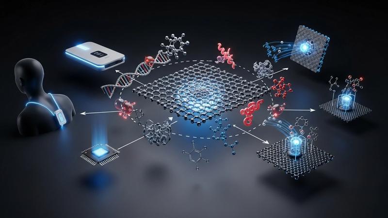
The future of graphene-based biological and chemical sensors hinges on leveraging its unparalleled intrinsic properties for increasingly sophisticated and integrated detection platforms. The ultra-high surface-to-volume ratio of single-layer graphene, coupled with its exceptionally high carrier mobility, often exceeding 15,000 cm^2/Vs at room temperature, provides an exquisite foundation for highly sensitive field-effect transistor (FET) architectures. These devices, when functionalized with specific recognition elements such as aptamers, antibodies, or molecularly imprinted polymers (MIPs), enable label-free, real-time detection of analytes with unprecedented limits of detection. For instance, aptamer-functionalized graphene FETs have demonstrated the capability to detect specific protein biomarkers, like thrombin or prostate-specific antigen, in complex biological matrices at femtomolar concentrations, far surpassing the sensitivity of conventional immunoassay techniques. Future advancements will focus on dense integration of these sensors into multiplexed arrays, facilitating simultaneous detection of dozens of analytes on a single chip, and seamless interfacing with microfluidic systems for automated sample preparation and delivery, ultimately leading to portable, point-of-care diagnostic devices with rapid turnaround times.
The high-value B2B applications of these advanced graphene sensors span critical sectors from precision medicine to pervasive environmental monitoring. In medical diagnostics, epidermal graphene patches, incorporating enzyme-functionalized biosensors, are progressing towards real-time glucose monitoring with sub-millisecond response times, offering a transformative alternative to traditional invasive methods. In neurobiology, flexible graphene electrode arrays enable direct in vivo monitoring of neurotransmitter fluctuations (e.g., dopamine, serotonin), opening new avenues for understanding neurological disorders. These sensors exploit graphene's low electrical resistivity (typically in the range of 10^-6 Ohm.cm) and biocompatibility for minimal tissue perturbation. For environmental applications, functionalized graphene oxide and reduced graphene oxide (rGO) electrodes excel in heavy metal detection and removal, empirically demonstrating adsorption efficiencies of up to 79% for lead and 72% for cadmium ions within minutes, enabling effective water purification and real-time contaminant sensing. In gas sensing, graphene's extreme surface sensitivity allows for ppb-level detection of hazardous industrial gases (e.g., NO2, NH3, H2S). Advanced sensor designs now incorporate localized thermal pulses, sometimes reaching 3000K for brief durations, to rapidly desorb analytes and regenerate sensor surfaces, ensuring long-term operational stability and reusability in harsh industrial environments.
Realizing the full commercial potential of graphene biological and chemical sensors necessitates addressing several engineering and scale-up challenges, primarily concerning selectivity enhancement, long-term stability in complex matrices, and cost-effective, high-throughput manufacturing. Future developments will focus on engineering heterostructures, such as graphene-MoS2 hybrids, to fine-tune electronic properties and enhance selective binding, alongside the integration of robust passivation layers to protect sensor elements from biofouling and degradation. The B2B value proposition is clear: these sensors promise to dramatically reduce operational costs associated with traditional laboratory analyses, accelerate decision-making processes through real-time data acquisition, and enable entirely new capabilities in predictive maintenance and personalized healthcare. For instance, pervasive sensor networks for infrastructure monitoring or agricultural yield optimization, where thousands of distributed graphene sensors continuously report data, will require sophisticated AI-driven analytics and cloud computing infrastructure. The ability of graphene sensors to provide immediate feedback, with reaction times measured in milliseconds, transforms reactive problem-solving into proactive management across industries. The confluence of advanced materials science, microelectronics, and data science is positioning graphene at the forefront of a paradigm shift towards ubiquitous, intelligent sensing, driving significant market penetration in diagnostics, environmental protection, and industrial process control.
Evaluate Our Quality
Serious about B2B integration? Test our premium Pulsed Electrical Resistive Carbon Heating turbostratic graphene in your lab. 100g sample packs available now.