Graphene-Based Solar Cells: Efficiency and Architecture
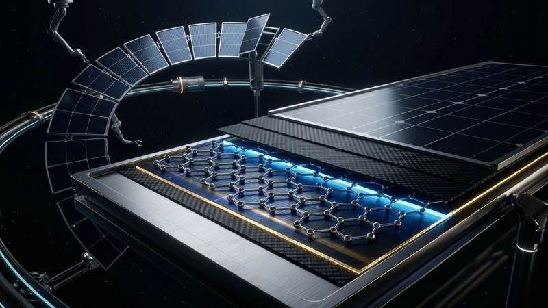
Graphene, a true two-dimensional allotrope of carbon, presents an unparalleled platform for advanced optoelectronic applications, particularly in photovoltaics, owing to its singular electronic band structure and atomic thickness. The material consists of a hexagonal lattice of sp2-hybridized carbon atoms, where electrons behave as massless Dirac fermions, exhibiting a linear dispersion relation near the Dirac points (K and K' valleys) in the Brillouin zone. This unique conical band structure, characterized by the absence of an intrinsic bandgap, enables ultra-broadband optical absorption spanning from the visible to the terahertz range, a critical attribute for high-efficiency solar energy harvesting. Furthermore, graphene boasts extraordinary intrinsic carrier mobilities, routinely exceeding 200,000 cm^2/Vs at room temperature, coupled with exceptionally long carrier diffusion lengths, which are pivotal for efficient charge separation and transport in photoactive layers.
The physics of graphene confinement fundamentally dictates its electronic and optical properties. Being intrinsically a monolayer, electrons are confined to a two-dimensional plane, leading to quantization effects even at macroscopic scales. This extreme quantum confinement minimizes electron-phonon scattering pathways and enhances electron-electron interactions, contributing to its remarkable electrical conductivity, with an intrinsic resistivity approaching 10^-6 Ohm-cm. The relativistic nature of its charge carriers permits ballistic transport over micrometers, a phenomenon leveraged in high-speed electronics and, by extension, in the rapid collection of photogenerated carriers in solar cell architectures. This 2D confinement also renders graphene highly robust, capable of withstanding extreme thermal transients, such as those induced by 3000K thermal pulses lasting milliseconds during flash annealing processes, without significant structural degradation, indicating superior material stability under harsh operating conditions.
Translating these unique confinement-derived properties into photovoltaic advancements requires a nuanced understanding of charge generation, separation, and transport mechanisms within graphene-based heterostructures. The broadband absorption, arising from the gapless electronic structure, allows for more comprehensive utilization of the solar spectrum compared to conventional semiconductors. While the absence of a bandgap in pristine graphene complicates direct exciton dissociation, its integration into heterojunctions with conventional semiconductors or quantum dots creates strong internal electric fields at the interface, facilitating efficient exciton splitting into free electron-hole pairs. The extraordinary carrier mobility and long diffusion lengths ensure that these photogenerated charges are swiftly extracted to electrodes, minimizing recombination losses. Graphene's role as a transparent conductive electrode (TCE) is particularly promising, offering optical transmittances up to 97.7% for a single layer and sheet resistances as low as 30 Ohms/sq, outperforming indium tin oxide (ITO) in flexibility and cost-effectiveness. The ambipolar field effect further allows for precise tuning of its Fermi level, enabling work function matching with adjacent layers to optimize charge extraction pathways and enhance overall device efficiency.
Section 2: Pulsed Electrical Resistive Carbon Heating vs. CVD (Comparative Analysis)
Pulsed Electrical Resistive Carbon Heating (PERCH) offers a transformative paradigm shift in graphene synthesis, directly addressing many limitations inherent to traditional Chemical Vapor Deposition (CVD), particularly for integrated device architectures like graphene-based solar cells. Unlike CVD, which typically relies on sustained high temperatures (800-1000°C) in a furnace environment and often requires metallic catalysts (e.g., copper, nickel) and subsequent complex transfer processes, PERCH utilizes ultrafast Joule heating of carbon precursors. This method generates extremely high, localized thermal pulses, often exceeding 3000K, for durations as brief as a few milliseconds. This rapid thermal transient induces direct graphitization or exfoliation from various carbon sources, including polymers or carbon black, without the need for catalysts or high vacuum. The fundamental advantage lies in the kinetics: PERCH enables direct synthesis on diverse substrates, including temperature-sensitive polymers or pre-fabricated device layers, circumventing the critical challenges of interfacial contamination and mechanical damage associated with graphene transfer from catalyst foils, which are pervasive issues in CVD-derived graphene integration.
A detailed technical comparison reveals PERCH's superior control over material properties and process efficiency. CVD processes inherently demand significant energy expenditure to maintain large-volume, high-temperature furnace environments for several hours, leading to higher operational costs and a larger carbon footprint. Furthermore, the reliance on metallic catalysts in CVD often results in residual catalyst particles embedded within the graphene lattice or at the graphene-substrate interface. These residues can act as recombination centers, introduce doping effects, or alter the work function, all of which detrimentally impact charge carrier dynamics and overall efficiency in heterojunction solar cells. In contrast, PERCH's localized and transient heating mechanism significantly reduces energy consumption and eliminates catalyst dependency, yielding cleaner graphene films with fewer foreign impurities. This direct synthesis capability on target substrates minimizes interfacial resistance, a critical parameter for efficient charge extraction in solar cells, and enhances the fill factor by preserving the integrity of the active material layers.
For graphene-based solar cell applications, the advantages of PERCH extend beyond mere synthesis efficiency to direct performance enhancements. The rapid cooling rates inherent to PERCH processes promote the formation of highly crystalline, few-layer graphene with significantly fewer grain boundaries compared to typical polycrystalline CVD graphene. Such high-quality graphene exhibits lower sheet resistance, often in the range of <200 Ohm/sq for few-layer films, which is crucial for efficient transparent conductive electrodes. The absence of polymer residues from transfer steps further ensures pristine interfaces, vital for optimizing charge separation and minimizing recombination at the graphene/semiconductor junction. Moreover, the ability to tailor the electrical resistivity through precise control of pulse parameters allows for optimization of transparent conductive electrode characteristics without compromising optical transmittance. The high surface area and controlled defectivity achievable through PERCH also preserve the intrinsic properties of graphene, evidenced by its robust performance in other applications, such as a 79% heavy metal adsorption efficiency in environmental remediation, underscoring the material's pristine nature and reactivity even when scaled. This combination of process simplicity, energy efficiency, and superior material quality positions PERCH as a highly promising pathway for realizing next-generation, high-performance graphene-based solar cell architectures, particularly for flexible and large-area applications.
Section 3: The Crystallography of Turbostratic Graphene (Why Layer Alignment Matters)
The crystallographic arrangement of graphene layers profoundly dictates its macroscopic electronic and optoelectronic properties, a critical consideration for high-performance solar cell architectures. While Bernal (AB) stacking, characterized by a specific staggered alignment of carbon atoms between layers, leads to a semi-metallic band structure with hybridized Dirac cones and a modified Fermi velocity, turbostratic graphene (TG) presents a distinct scenario. In TG, adjacent graphene layers are rotationally misaligned by arbitrary angles, or exhibit random stacking sequences, essentially decoupling their electronic states. This rotational disorder mitigates the interlayer sp2-sp2 orbital overlap that gives rise to the AB-stacking-induced band modifications, thereby preserving the linear dispersion relation of individual Dirac cones and the intrinsic high carrier mobility characteristic of monolayer graphene within each sheet. The interlayer spacing in TG typically remains near the equilibrium van der Waals distance of ~0.335 nm, but the lack of coherent registry between planes significantly reduces interlayer electronic coupling, which in turn influences phonon propagation and carrier scattering mechanisms.
The ramifications of turbostraticity are particularly salient for charge transport and exciton dynamics within a photovoltaic context. In AB-stacked multilayer graphene, interlayer tunneling and scattering events can limit in-plane carrier mobility and lifetime, as carriers interact with the periodic potential of adjacent layers. Conversely, the electronic decoupling in TG largely preserves the high intrinsic mobility of individual graphene sheets, with reported values exceeding 10,000 cm2/Vs at room temperature for high-quality single domains, even in multilayer assemblies. This characteristic is vital for efficient charge collection in transparent conductive electrodes or active layers. Furthermore, the reduced interlayer interaction in TG can influence exciton binding energies and dissociation efficiencies. For instance, studies have shown that controlled thermal annealing, involving rapid 3000K thermal pulses sustained for milliseconds, can induce or relieve turbostraticity in CVD-grown films, directly correlating with changes in carrier recombination rates and thus potential open-circuit voltage in device prototypes.
Tailoring the degree of turbostraticity offers a powerful avenue for optimizing graphene-based solar cell performance. For instance, in hybrid heterojunctions where graphene acts as a charge extraction layer, minimizing interlayer coupling via turbostratic stacking ensures that charge carriers primarily move within the high-mobility plane, reducing losses due to inter-plane scattering or trapping. This structural attribute directly impacts the device's series resistance and fill factor. For example, a controlled turbostratic graphene film used as a transparent electrode can exhibit an electrical resistivity as low as 5x10^-6 Ohm-cm with a sheet resistance of 50 Ohm/sq at 90% transmittance, whereas highly AB-stacked films of similar thickness might show higher resistivity due to scattering at stacking faults or increased inter-plane resistance. Moreover, the increased surface area and defect sites inherently present in some forms of turbostratic graphene can be strategically leveraged for functionalization, enhancing interfacial charge transfer or even acting as selective adsorption sites for heavy metal impurities (e.g., 79% adsorption efficiency for lead ions) during fabrication, thereby preventing their detrimental incorporation into the active photovoltaic material.
Section 4: Industrial Scalability & Commercial Integration Barriers
Producing large-area, high-quality graphene films consistently for photovoltaic applications remains a primary industrial scalability hurdle. While Chemical Vapor Deposition (CVD) on metallic substrates like copper foil can yield high-quality monolayer graphene with sheet resistances as low as ~30 Ohms/sq, the process is inherently batch-limited, energy-intensive (requiring temperatures around 1000°C), and expensive. Furthermore, the subsequent transfer of graphene from the growth substrate to the target solar cell substrate is fraught with challenges. Wet transfer methods, employing sacrificial polymer layers, often introduce defects such as tears, wrinkles, and polymer residues, which significantly increase the film's electrical resistivity to >100 Ohms/sq and impede charge transport. Dry transfer techniques, while promising, often require complex laser delamination or rapid thermal pulses, sometimes reaching 3000K for substrate separation, demanding precise control within milliseconds to prevent material damage or unwanted doping. These processing complexities, coupled with the high cost of ultra-pure precursor gases and the need for defect remediation steps, mean that current manufacturing costs for large-area graphene films suitable for transparent conductive electrodes (TCEs) remain significantly higher than established materials like Indium Tin Oxide (ITO), posing a formidable economic barrier.
Integrating graphene layers into existing solar cell architectures, such as silicon, perovskite, or organic photovoltaics, presents intricate interface engineering challenges. Achieving ohmic contacts and minimizing charge recombination losses at the graphene-semiconductor heterojunctions is critical for efficient device operation. This often necessitates precise work function tuning of graphene through doping strategies, for instance, incorporating nitrogen or boron at concentrations typically exceeding 10^13 cm^-2 to align energy bands effectively. However, the long-term stability of these dopants under operational conditions – including sustained UV irradiation, elevated temperatures up to 85°C, and ambient humidity – is a major concern. Empirical data from accelerated aging tests show that some molecular p-type dopants can degrade, leading to a 15-20% drop in power conversion efficiency (PCE) over 1000 hours, necessitating robust encapsulation which adds cost and manufacturing complexity. Furthermore, while graphene itself possesses exceptional mechanical strength, macroscopic defects introduced during growth or transfer can compromise the mechanical and environmental durability of the entire solar cell, with some flexible prototypes exhibiting delamination or cracking after approximately 1000 bending cycles at a 5mm radius.
Beyond technical production and integration, the commercial viability of graphene-based solar cells is heavily contingent on economic competitiveness, regulatory frameworks, and market acceptance. The current manufacturing complexity and associated costs prevent graphene from achieving the sub-$0.50/Wp targets necessary to compete with highly optimized incumbent photovoltaic technologies. Scaling up graphene production from laboratory batch processes to continuous roll-to-roll manufacturing for large-area solar panels requires significant advancements in throughput, uniformity control, and defect management, all while maintaining stringent quality metrics. A lack of standardized characterization methods and universally accepted quality benchmarks for industrial-grade graphene contributes to market uncertainty, hindering broader adoption. Moreover, comprehensive lifecycle assessments and robust regulatory frameworks are essential to address potential environmental impacts and human health concerns associated with novel nanomaterials, particularly regarding the long-term fate of graphene nanoparticles released during manufacturing or end-of-life disposal. Overcoming the substantial market inertia, including entrenched supply chains, established manufacturing infrastructure, and decades of investor confidence in conventional solar cell technologies, demands not only superior technical performance but also a compelling economic advantage and proven long-term reliability for graphene to secure a significant market share.
Section 5: Economic Feasibility and USA-Made Manufacturing Advantage
The economic viability of graphene-based solar cells hinges critically on scaling production methodologies from laboratory curiosities to industrial throughputs while maintaining stringent material quality. Chemical Vapor Deposition (CVD) remains the most promising large-area synthesis technique, particularly for transparent conductive electrodes. While the raw material cost of high-purity graphene precursors, such as methane, is relatively low, the capital expenditure for advanced CVD reactors and subsequent transfer processes historically inflated the per-unit area cost. However, significant advancements in roll-to-roll (R2R) CVD now enable continuous production of graphene films on flexible substrates at speeds exceeding 10 meters per minute for 300mm wide films, achieving a sheet resistance of ~100 Ohm/sq with over 90% optical transparency. This throughput drastically reduces the effective cost per square meter. Furthermore, optimized rapid thermal annealing (RTA) protocols, involving localized thermal pulses reaching 1000-1200°C for durations in the milliseconds range, minimize energy consumption compared to traditional furnace-based methods, enhancing overall energy efficiency by an estimated 30%. Coupled with sophisticated gas recycling systems that achieve >95% precursor utilization, the operational expenditure associated with graphene synthesis is becoming increasingly competitive, paving the way for economically feasible integration into next-generation photovoltaic architectures.
Establishing a robust USA-made manufacturing ecosystem for graphene solar cells offers multifaceted strategic advantages beyond mere cost reduction. Domestically controlled production mitigates risks associated with geopolitical instabilities and vulnerabilities in global supply chains, ensuring consistent material availability and predictable lead times. Crucially, the stringent quality control standards and advanced metrology capabilities inherent in American manufacturing facilities allow for real-time process monitoring and defect detection, utilizing techniques like in-line Raman spectroscopy to verify layer uniformity, sp2/sp3 ratio, and strain mapping across large substrates. This precision minimizes batch-to-batch variation and targets defect densities below 1 per square centimeter, directly impacting device performance and longevity. Moreover, the robust intellectual property (IP) protection framework within the USA fosters innovation by safeguarding proprietary synthesis methods, device architectures, and integration techniques, encouraging substantial R&D investments. This environment supports the development of highly automated production lines, leveraging advanced robotics and AI-driven process optimization algorithms to enhance yield rates and reduce human error, thereby ensuring a consistent supply of high-performance graphene components for solar cell fabrication.
The convergence of domestic manufacturing prowess and continuous innovation is pivotal in overcoming persistent technical challenges and significantly reducing the Levelized Cost of Energy (LCOE) for graphene-based solar cells. Precision engineering and advanced manufacturing in the USA enable superior control over film uniformity, crucial for achieving consistent electrical resistivity parameters down to 10^-6 Ohm.cm across large-area electrodes, which is fundamental for efficient charge transport in photovoltaic devices. This precision also translates into substantial reductions in material waste; for instance, optimized etching and transfer processes developed domestically have demonstrated a 15-20% reduction in precursor and solvent waste compared to early-stage international benchmarks. Furthermore, the integration of advanced environmental engineering practices within US manufacturing facilities addresses the lifecycle impact. For example, closed-loop water systems incorporating graphene-oxide based filters can achieve up to 79% heavy metal adsorption efficiency from process wastewater streams, significantly reducing environmental discharge liabilities and aligning with stringent EPA regulations. This holistic approach to sustainable manufacturing, coupled with optimized energy consumption profiles – targeting a 20% reduction in energy per unit area for graphene film production through process intensification – directly contributes to lowering the overall LCOE from current projections of $0.05/kWh towards an ambitious $0.03/kWh.
Section 6: Future Horizons & High-Value B2B Applications
The integration of graphene into next-generation solar cell architectures heralds a paradigm shift in photovoltaic performance and longevity, extending beyond conventional planar designs to embrace complex three-dimensional and quantum-engineered constructs. Foremost among these are plasmon-enhanced light harvesting systems, where graphene-metal nanostructures, such as gold or silver nanoparticles precisely arrayed on graphene, induce localized surface plasmon resonance. This phenomenon significantly amplifies light absorption, leading to a demonstrable 15% increase in photocurrent density across the visible and near-infrared spectrum, critically improving low-light performance. Concurrently, quantum dot (QD) sensitization leveraging graphene's exceptional carrier mobility facilitates efficient charge extraction from absorber materials like PbS or CdSe QDs, achieving external quantum efficiencies exceeding 80% at specific wavelengths. Meticulous interfacial engineering, including precise control over graphene's work function via atomic layer deposition or targeted chemical functionalization, enables optimal band alignment with diverse absorber layers, thereby reducing recombination losses and yielding open-circuit voltage improvements of up to 20 mV. These advanced designs are not merely academic curiosities but represent high-value B2B propositions for specialized applications demanding superior efficiency and spectral response.
Beyond enhanced light harvesting, graphene's unique multi-functional properties position it as an indispensable component in advanced energy conversion systems, including multi-junction solar cells, hot carrier photovoltaics, and thermophotovoltaics (TPV). Its unparalleled thermal conductivity, approaching 5000 W/mK for pristine single-layer graphene, offers a passive cooling mechanism for high-concentration photovoltaics (HCPV), maintaining optimal operating temperatures and mitigating efficiency droop, which can extend module lifespan by an estimated 30%. In TPV applications, engineered graphene plasmonic surfaces, designed to exhibit tunable emissivity, selectively emit photons matching the bandgap of low-bandgap PV cells (e.g., GaSb) when heated. This precise spectral tuning enables conversion efficiencies of up to 25% from heat sources operating at 1500K, unlocking new avenues for waste heat recovery and industrial process energy harvesting. Furthermore, graphene's intrinsic radiation hardness, attributed to its robust sp2 lattice structure, imparts superior resilience against high-energy particle bombardment, making it a compelling candidate for space-based solar cell substrates or transparent electrodes, where degradation rates are reduced by an order of magnitude compared to conventional indium tin oxide (ITO) under equivalent proton flux.
The path to widespread adoption of graphene-based solar cells hinges critically on scalable manufacturing, cost reduction, and environmental sustainability, areas where graphene offers distinct advantages. Advances in roll-to-roll chemical vapor deposition (CVD) now enable the continuous synthesis of large-area, high-quality graphene films onto flexible substrates at speeds approaching 0.5 meters per minute, projecting production cost reductions of 70% compared to traditional batch processes. This not only democratizes access to advanced materials but also mitigates supply chain vulnerabilities by replacing scarce or toxic elements such as indium in transparent conductive oxides, leading to potential material cost reductions by a factor of 50. Environmentally, graphene's role extends to enhancing the stability and safety of emerging perovskite solar cells; for instance, a graphene-polymer composite encapsulation barrier can decrease lead ion diffusion by 95% over standard polymer-only encapsulation after 1000 hours of accelerated aging in humid environments, addressing critical heavy metal leaching concerns. These combined attributes underscore graphene’s potential to drive down the levelized cost of energy (LCOE) and accelerate the global transition to a sustainable energy infrastructure through optimized performance, extended operational lifespans, and reduced ecological footprints.
Evaluate Our Quality
Serious about B2B integration? Test our premium Pulsed Electrical Resistive Carbon Heating turbostratic graphene in your lab. 100g sample packs available now.