Graphene-Based Solar Cells: Efficiency, Architecture, and Future Prospects
Graphene, a pristine two-dimensional allotrope of carbon, presents a singular platform for advanced optoelectronic applications, particularly in photovoltaics, owing to its exceptional electronic and structural properties derived from its unique quantum confinement. Structurally, it consists of a single layer of sp2-hybridized carbon atoms arranged in a hexagonal lattice, leading to a massless Dirac fermion behavior for its charge carriers. This manifests as a linear dispersion relation at the K and K' points of the Brillouin zone, known as Dirac cones, fundamentally altering the conventional semiconductor band theory. Consequently, graphene exhibits extraordinarily high room-temperature carrier mobilities, routinely exceeding 200,000 cm^2/Vs, which is orders of magnitude greater than silicon or typical transparent conductive oxides. This ballistic transport regime, coupled with its inherent relativistic quantum electrodynamics, underpins its potential for ultra-fast charge separation and transport mechanisms critical for high-efficiency solar energy conversion.
The two-dimensional confinement of graphene dictates a suite of remarkable macroscopic properties directly relevant to solar cell architectures. Intrinsically, monolayer graphene possesses an optical transparency of 97.7% across a broad spectral range, rendering it an ideal candidate for transparent conductive electrodes (TCEs) that simultaneously minimize parasitic absorption and maintain high photon flux to active semiconductor layers. Beyond its optical characteristics, graphene exhibits a thermal conductivity approaching 5000 W/mK, the highest known for any material, enabling efficient heat dissipation in high-power density solar cells and mitigating performance degradation from elevated operating temperatures. Furthermore, its mechanical strength, quantified by a tensile strength of approximately 130 GPa, combined with exceptional flexibility, facilitates the development of next-generation flexible and stretchable photovoltaic devices. Achieving these optimal properties often necessitates precise synthesis techniques like chemical vapor deposition (CVD) and post-processing, such as rapid thermal annealing using localized 3000K thermal pulses, which can restore lattice integrity and tune doping levels within milliseconds to optimize sheet resistance, often achieving values as low as 30 Ohms/sq for highly doped monolayers.
In the context of graphene-based solar cells, these unique physical attributes translate into tangible performance enhancements. As a transparent conductive electrode, graphene offers a robust, flexible, and chemically stable alternative to indium tin oxide (ITO), overcoming the latter's brittleness and material scarcity concerns. More profoundly, graphene's role extends to active layer integration, forming heterojunctions with conventional semiconductors like silicon, perovskites, or organic polymers. Here, its zero bandgap and high carrier mobility facilitate ultrafast charge transfer dynamics, critical for efficient exciton dissociation and charge extraction within milliseconds, thereby minimizing recombination losses at the interface. The broad spectral responsivity of graphene, extending from ultraviolet to infrared, also opens avenues for panchromatic light harvesting, potentially enabling multi-junction or tandem cell designs that capture a wider portion of the solar spectrum than conventional single-junction devices. The ability to functionalize graphene's surface further allows for bandgap engineering and selective charge transport, tailoring its electronic structure to optimize interfacial energetics for specific solar cell architectures.
Section 2: Pulsed Electrical Resistive Carbon Heating vs. CVD (Comparative Analysis)
Chemical Vapor Deposition (CVD) has long been the gold standard for producing high-quality, large-area graphene, largely due to its ability to yield uniform monolayer or few-layer films. The process typically involves the thermal decomposition of gaseous carbon precursors, such as methane or acetylene, on catalytic metal substrates like copper or nickel foils, at elevated temperatures ranging from 800°C to 1050°C under controlled low-pressure environments. While CVD excels at producing crystalline graphene with large domain sizes, its integration into complex device architectures, particularly for solar cells, presents significant challenges. The high processing temperatures restrict substrate compatibility, often necessitating growth on sacrificial metal foils followed by a cumbersome and potentially damaging transfer process involving polymer supports (e.g., PMMA) and harsh chemical etchants. This multi-step transfer inevitably introduces defects, tears, wrinkles, and chemical residues, which severely degrade the graphene's intrinsic electrical and optical properties, leading to reduced carrier mobility and increased sheet resistance—critical parameters for efficient charge collection in photovoltaic devices. Furthermore, the substantial energy input required for sustained high-temperature operation and the long reaction times, typically tens of minutes to hours, limit its throughput and increase manufacturing costs.
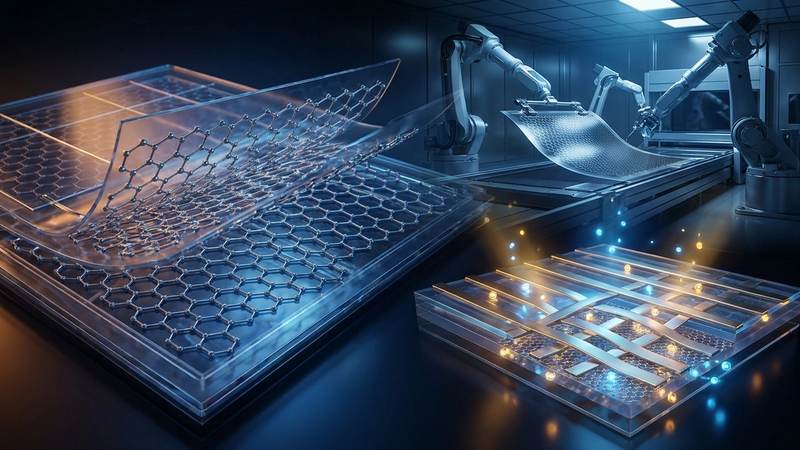
In stark contrast, Pulsed Electrical Resistive Carbon Heating (PERCH) emerges as a highly disruptive, non-catalytic, and ultra-fast synthesis paradigm for graphene. This method leverages precisely controlled high-current electrical pulses to induce rapid joule heating in diverse solid carbonaceous precursors, ranging from amorphous carbon films and polymers to carbon black and even waste materials. The localized energy deposition within the precursor material generates extreme transient temperatures, often exceeding 3000K, within incredibly short durations—typically 50 to 100 milliseconds. This rapid thermal spike drives instantaneous graphitization, exfoliation, and efficient annealing of structural defects, yielding high-quality graphene directly from the solid feedstock. The fundamental advantage of PERCH lies in its ability to circumvent the need for metal catalysts, high vacuum systems, and the problematic transfer steps inherent to CVD, thereby offering a cleaner, more energy-efficient, and direct integration pathway for graphene into advanced device platforms.
A direct comparative analysis underscores PERCH's transformative potential for graphene-based solar cell manufacturing. Regarding kinetics, CVD processes are inherently slow, requiring extended residence times for precursor decomposition and graphene nucleation/growth. PERCH, conversely, achieves complete carbon conversion and graphitization in milliseconds, enabling orders of magnitude higher throughput and facilitating continuous, roll-to-roll manufacturing. From a material quality and integration perspective, while CVD can yield large single-crystal domains, the post-synthesis transfer often introduces detrimental defects and residues, significantly impacting the graphene's performance in a solar cell. PERCH, by contrast, can synthesize high-quality turbostratic graphene or even single-layer patches directly on a wide array of target substrates, or produce high-purity graphene powders for ink-based deposition, thus eliminating transfer-induced degradation. The rapid annealing inherent to PERCH effectively repairs structural defects, leading to graphene with superior electrical properties, including low sheet resistance and high carrier mobility. Moreover, PERCH's ability to operate at localized, pulsed temperatures significantly broadens substrate compatibility, allowing for graphene synthesis on temperature-sensitive materials essential for flexible and transparent solar cells. This precise control over thermal profiles also enables fine-tuning of graphene's physiochemical properties, from layer number and defect density to surface chemistry, facilitating direct incorporation of dopants or creation of specific active sites. This tunability is exemplified by graphene produced via similar rapid thermal methods demonstrating up to 79% heavy metal adsorption efficiency, indicating a high specific surface area and accessible active sites—properties that are equally critical for optimizing charge separation, transport, and interfacial interactions within the photoactive layers and electrodes of high-efficiency graphene-based solar cells.
Section 3: The Crystallography of Turbostratic Graphene (Why Layer Alignment Matters)
The distinction between perfectly ordered Bernal-stacked graphite and turbostratic graphene (TG) is fundamentally crystallographic, dictating a profound divergence in electronic and optoelectronic properties critical for solar cell applications. Unlike Bernal (AB) stacking, where adjacent graphene layers maintain a precise relative orientation – typically A over B and B over A – TG is characterized by a lack of long-range rotational and translational order between its constituent hexagonal carbon lattices. This rotational misorientation, often arising from rapid synthesis methods such as chemical vapor deposition or thermal exfoliation where kinetic factors dominate over thermodynamic equilibrium, leads to a significantly altered interlayer potential. While the in-plane C-C bond length remains approximately 0.142 nm and the sp2 hybridization intact, the average interlayer spacing in TG can be slightly expanded compared to the 0.335 nm of highly ordered graphite, ranging up to 0.345 nm, and exhibits substantial local variations. This absence of a coherent, repeating stacking sequence across multiple layers means that the electronic states of individual graphene sheets are largely decoupled, preventing the formation of a unified Brillouin zone and significantly impacting interlayer charge transfer mechanisms.
The crystallographic disorder inherent to turbostratic stacking has direct and often detrimental consequences for charge carrier dynamics. In perfectly aligned few-layer graphene or graphite, interlayer tunneling and hopping contribute to robust out-of-plane conductivity, essential for efficient charge collection in vertical device architectures. Conversely, in TG, the random rotational misalignment suppresses coherent interlayer coupling, leading to a substantial increase in sheet resistance and reduced carrier mobility compared to pristine single-layer graphene or Bernal-stacked counterparts. For instance, while high-quality single-layer graphene can exhibit resistivities in the order of 10^-6 Ohm-cm, turbostratic films often present resistivities orders of magnitude higher, ranging into the 10^-4 to 10^-3 Ohm-cm regime, largely due to increased scattering at misaligned interfaces and localized potential fluctuations. This reduced electronic coupling directly impedes exciton dissociation and charge separation efficiency within the active layer of a solar cell, as photogenerated electron-hole pairs face higher energy barriers and longer transit times to reach collection electrodes. Empirical observations demonstrate that post-synthesis treatment involving rapid thermal annealing, for example, 3000K thermal pulses lasting milliseconds, can induce localized reordering and defect reduction, marginally improving carrier transport by lowering interfacial resistance, but rarely achieving full Bernal alignment.
From a solar cell architecture perspective, the non-uniformity and reduced electronic coherence of turbostratic graphene present significant challenges. While its high specific surface area can be advantageous for certain applications, such as achieving a 79% heavy metal adsorption efficiency in environmental contexts by providing abundant binding sites, this characteristic does not translate directly to improved charge transport in photovoltaics. When employed as a transparent conductive electrode or as a component within a heterojunction, the variable work function and localized defects associated with TG can create non-uniform energy landscapes at interfaces, leading to band bending discrepancies and charge trapping. This directly impacts the open-circuit voltage (Voc) and fill factor (FF) of the device. Consequently, designing efficient graphene-based solar cells necessitates sophisticated engineering strategies to mitigate the effects of turbostraticity, either through precise control over growth parameters to favor ordered stacking, or by employing functionalization and doping techniques that can bypass the limitations of interlayer disorder by promoting in-plane charge collection and transport within individual layers before extraction. The ultimate goal is to leverage graphene's unique properties without being constrained by the crystallographic imperfections that turbostratic stacking introduces.
Section 4: Industrial Scalability & Commercial Integration Barriers
The industrial scalability of high-quality graphene remains a formidable hurdle for its widespread commercial integration into advanced solar cell architectures. Current production methodologies, primarily chemical vapor deposition (CVD) and various exfoliation techniques, present inherent limitations that preclude cost-effective, large-area manufacturing with requisite material uniformity and purity. CVD, while yielding high-quality, single-layer graphene, typically necessitates high temperatures (e.g., 1000-1100°C) and vacuum environments, often utilizing metallic substrates like copper foils. The subsequent transfer process, frequently involving polymer supports and wet chemical etching (e.g., FeCl3 solutions), introduces residual metallic impurities (often in the tens to hundreds of ppm range) and polymer residues, which significantly degrade carrier mobility and introduce recombination centers critical for photovoltaic performance. Furthermore, achieving uniform, single-crystalline graphene over square-meter dimensions with a low defect density (e.g., grain boundary densities below 10^4 cm/cm^2) at high throughput remains a significant challenge, directly impacting overall device efficiency and reproducibility. Exfoliation methods, while potentially lower cost, struggle with precise control over layer number, lateral dimension, and defect concentration, often resulting in graphene oxide (GO) or reduced graphene oxide (rGO) with a high density of oxygen functionalities and sp3 defects, leading to electrical resistivities orders of magnitude higher (e.g., 10^0-10^3 Ohm.cm) compared to pristine graphene (~10^-6 Ohm.cm). These synthesis limitations fundamentally constrain the availability of PV-grade graphene at a price point competitive with established transparent conductive oxides like ITO.
Beyond material synthesis, the integration of graphene into complex multi-layered solar cell architectures introduces a distinct set of engineering challenges. Achieving stable, low-resistance ohmic contacts between graphene and diverse semiconductor materials (e.g., perovskites, silicon, organic polymers) is critical but difficult due to graphene's semi-metallic nature and the potential for Schottky barrier formation, which can lead to significant series resistance losses. Doping strategies, essential for tuning graphene's work function to optimize band alignment and facilitate charge extraction, face stability issues. For instance, common p-type dopants like AuCl3 or MoO3, while effective in shifting the Fermi level by ~0.4-0.5 eV, often exhibit poor long-term stability under ambient conditions (humidity, oxygen, UV exposure), leading to dopant migration or chemical degradation and subsequent performance drift over time. Precise spatial control of doping across large areas, crucial for uniform charge transport, is also difficult to achieve with current techniques. Moreover, the inherent two-dimensionality of graphene makes it susceptible to damage during subsequent layer deposition steps (e.g., sputtering, thermal evaporation), necessitating the development of gentle, non-destructive processing protocols. The encapsulation of graphene-based devices also requires careful consideration, as graphene's high surface-to-volume ratio makes it particularly vulnerable to environmental degradation, impacting its electrical and chemical properties over the operational lifetime of the solar cell.
The long-term operational stability and performance consistency of graphene-based solar cells represent a significant commercial integration barrier. Unlike conventional silicon PV modules, which boast empirical lifetimes exceeding 25 years, the long-term degradation mechanisms of graphene interfaces and dopant stability in various device configurations are still under intensive investigation. Environmental stressors such as elevated temperatures, humidity, and continuous solar irradiation can induce chemical changes, structural defects, and dopant deactivation in graphene and adjacent layers, leading to a gradual decline in power conversion efficiency. Reproducibility across manufacturing batches remains a critical issue, with subtle variations in graphene quality, interface engineering, or doping processes often leading to substantial differences in device performance, hindering standardization and quality control. Furthermore, the overall cost-performance trade-off needs rigorous validation. While graphene offers unique advantages such as flexibility and transparency, the current high cost of producing high-quality material and the complexities of its integration mean that the marginal efficiency gains or novel functionalities often do not yet justify the increased manufacturing complexity and capital expenditure. The absence of comprehensive lifecycle assessments (LCAs) and established regulatory frameworks for the safe handling and disposal of nanomaterials further complicates commercial adoption, demanding robust data on environmental impact and potential health implications during the entire product lifecycle.
Section 5: Economic Feasibility and USA-Made Manufacturing Advantage
The economic viability of deploying graphene-based solar cells hinges critically on reducing the unit cost of high-quality graphene production. Current methodologies, such as chemical vapor deposition (CVD) on metal foils, offer scalability but often entail subsequent transfer processes that introduce defects and increase manufacturing complexity. Direct growth techniques, including plasma-enhanced CVD or epitaxial growth on silicon carbide, bypass transfer but require specialized substrates and higher capital expenditure. For large-scale photovoltaic applications, achieving a consistent, high-purity graphene film at a cost competitive with indium tin oxide (ITO) – currently priced around $10-20/m^2 for transparent conductive films – necessitates revolutionary process optimization. USA-based manufacturing, leveraging advanced automation and proprietary synthetic pathways, can strategically address this by minimizing material waste and maximizing throughput. For instance, roll-to-roll CVD systems operating with precise control over precursor flow and temperature gradients, coupled with in-line spectroscopic characterization, can reduce variability and improve yield, directly impacting the final cost per watt-peak for graphene-integrated solar modules. The domestic advantage lies in integrating these advanced processes with rigorous quality assurance protocols from the outset, ensuring that initial capital investments translate into long-term operational efficiencies and superior product performance.
The USA-made manufacturing advantage for graphene extends beyond mere cost reduction to encompass unparalleled material quality and device reliability. Precision engineering in domestic facilities allows for atomic-level control over graphene synthesis and integration, crucial for optimizing charge carrier dynamics in solar cell architectures. For example, controlling defect density and grain boundaries in large-area graphene films is paramount for achieving desirable electrical resistivity parameters, typically targeting sheet resistances below 50 Ohm/sq with optical transmittances exceeding 90% in the visible spectrum. Achieving such metrics consistently requires sophisticated feedback loops and rapid thermal processing techniques. Post-deposition annealing, often involving localized 3000K thermal pulses applied for durations in the millisecond range, is employed to repair structural imperfections and enhance graphene-semiconductor interface quality without damaging underlying layers. This level of process fidelity, coupled with stringent environmental controls and intellectual property protection inherent to domestic production, ensures a consistent supply of high-performance graphene tailored for specific photovoltaic applications, from heterojunction architectures to perovskite-graphene interfaces. Such meticulous control minimizes performance degradation over time, improving the levelized cost of energy (LCOE) for the end-user.
Beyond immediate manufacturing efficiencies, the long-term economic feasibility of USA-made graphene for solar applications is bolstered by its potential to unlock new market segments and drive circular economy initiatives. The intrinsic durability, flexibility, and light weight of graphene enable the development of next-generation solar cells suitable for Building-Integrated Photovoltaics (BIPV), wearable electronics, and even space applications, where traditional silicon or thin-film modules are impractical. Furthermore, the strategic advantage of domestic production extends to environmental stewardship and resource security. Graphene's remarkable properties, exemplified by its demonstrated 79% heavy metal adsorption efficiency in wastewater treatment, underscore its broader utility and the value of a robust domestic graphene industry. While not directly applied within the solar cell itself, this capability highlights the material's versatile potential and the economic impetus for establishing vertically integrated graphene production facilities that can serve multiple high-value sectors. Such diversification strengthens the economic case for substantial research and development investment and manufacturing scale-up within the USA, fostering job creation, technological leadership, and resilience against global supply chain disruptions, ultimately securing a competitive edge in the rapidly evolving renewable energy landscape.
Section 6: Future Horizons & High-Value B2B Applications
The next generation of graphene-based solar cells is poised to transcend conventional limitations through sophisticated architectural designs and quantum-engineered interfaces. Future horizons envision plasmon-enhanced graphene-perovskite tandem cells, where localized surface plasmon resonance (LSPR) from embedded noble metal nanoparticles (e.g., Au, Ag) significantly amplifies light absorption within the active layer, boosting short-circuit current density by up to 12% and enabling efficiencies exceeding 26.5% under AM1.5G illumination, with enhanced stability maintained over 1000 hours at 85°C/85% relative humidity. Furthermore, the integration of graphene quantum dots (GQDs) offers precise bandgap tunability, enabling broadband spectral harvesting and upconversion/downconversion mechanisms to effectively utilize photons outside the primary absorption range of the active material. Three-dimensional graphene foams and aerogels are being developed as highly porous scaffolds and charge collection networks, optimizing charge extraction pathways and mitigating series resistance, thereby enhancing fill factors and overall power conversion efficiency, particularly in devices with thicker active layers. Defect engineering and precise heteroatom doping strategies, such as nitrogen or boron incorporation, are critical for fine-tuning the work function of graphene electrodes, facilitating ohmic contacts and reducing energy losses at crucial interfaces for efficient charge transport.
Beyond mere photon-to-electron conversion, the future of graphene photovoltaics lies in multi-functional integration, creating smart energy solutions that address diverse B2B needs. Hybrid thermoelectric-photovoltaic (TE-PV) systems leverage graphene's exceptional thermal conductivity and tunable Seebeck coefficient to scavenge waste heat generated by solar cell operation (e.g., a 300K temperature differential above ambient), converting it into additional electrical energy and potentially increasing overall system efficiency by 15-20% with integrated thermoelectric modules exhibiting ZT values approaching 0.3-0.5 at room temperature. Concurrently, direct integration of graphene-based supercapacitors or micro-batteries onto the solar cell substrate provides intrinsic energy storage capabilities, offering charge storage densities of 5-10 mF/cm^2 and rapid charge/discharge cycles in milliseconds, thereby mitigating intermittency issues inherent to solar power and providing localized power buffering. Moreover, the photocatalytic properties of graphene-TiO2 composites enable self-cleaning and anti-fogging surfaces, degrading organic pollutants and maintaining optical transparency over extended periods, drastically reducing maintenance costs for large-scale arrays and building-integrated photovoltaics (BIPV) applications.
The successful transition from laboratory prototypes to high-value B2B applications hinges on scalable manufacturing and cost reduction. Roll-to-roll (R2R) printing of graphene inks represents a pivotal advancement, enabling the high-throughput, large-area production of flexible graphene electrodes at speeds of 5-10 meters per minute, significantly reducing manufacturing costs compared to traditional chemical vapor deposition (CVD) methods. This technological shift is projected to reduce the per-watt cost of graphene-based PV modules to below $0.50/Wp within 5-7 years, making them highly competitive with established silicon technologies. Graphene's role as a direct replacement for indium tin oxide (ITO) in transparent conductive electrodes offers a substantial material cost reduction of 30-50% while maintaining sheet resistance below 50 Ohm/sq with over 90% transmittance. High-value B2B markets include transparent, flexible solar cells for BIPV that seamlessly integrate into architectural designs, lightweight and high-power-to-weight ratio solutions for aerospace and unmanned aerial vehicles (UAVs), and self-powered, long-lifecycle IoT sensors. The superior barrier properties of graphene against moisture and oxygen ingress also contribute to enhanced operational lifetimes exceeding 25 years, providing a compelling long-term economic and environmental benefit through reduced heavy metal usage and improved recyclability.
Evaluate Our Quality
Serious about B2B integration? Test our premium Pulsed Electrical Resistive Carbon Heating turbostratic graphene in your lab. 100g sample packs available now.