Graphene-Based Solar Cells: Architecture and Efficiency
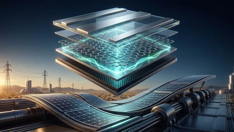
Graphene, a singular atomic layer of sp2-hybridized carbon atoms arranged in a hexagonal lattice, represents the archetypal two-dimensional (2D) material whose electronic structure dictates profoundly unique optoelectronic properties critical for advanced photovoltaics. Its exceptional charge carrier mobility, exceeding 200,000 cm2/Vs at room temperature, stems from its linear energy dispersion relation near the Dirac points, where electrons and holes behave as massless Dirac fermions. This relativistic quantum behavior, coupled with an intrinsic absence of a bandgap in pristine monolayer graphene, enables broadband optical absorption spanning from ultraviolet to terahertz frequencies, albeit with a modest ~2.3% absorption per layer across the visible spectrum. The fundamental physics of graphene confinement, primarily its single-atom thickness, is the genesis of these extraordinary characteristics, offering an unparalleled platform for manipulating charge dynamics in energy harvesting applications.
The true power of graphene in solar cell architectures lies not merely in its intrinsic properties but in the precise engineering of its quantum confinement effects. While pristine graphene lacks a bandgap, its 2D nature allows for strategic modification to induce one, a prerequisite for efficient photon-to-electron conversion. This is achieved through various methods, including quantum confinement effects in graphene nanoribbons (GNRs) where width dictates the bandgap, or in graphene quantum dots (GQDs) where lateral dimensions and edge passivation control the electronic states. Furthermore, the introduction of defects, heteroatom doping (e.g., nitrogen or boron), or functionalization can perturb the Dirac cone, opening a tunable bandgap and creating localized states that enhance light absorption and facilitate exciton generation. This ability to tailor the electronic structure through dimensional confinement and chemical modification is paramount for optimizing the material as an active layer, charge transport layer, or transparent conductive electrode within complex photovoltaic devices.
Optimizing graphene's role in solar cells necessitates meticulous control over its defect density, doping profile, and surface chemistry to manage charge separation and transport efficiently. For instance, advanced fabrication and post-processing techniques, such as localized 3000K thermal pulses, are employed to repair lattice defects or induce precise dopant incorporation within milliseconds. These high-temperature, rapid thermal annealing processes are critical for fine-tuning graphene's electrical resistivity, achieving sheet resistances below 100 Ω/sq for transparent conductive electrodes or bulk resistivities approaching 10-4 Ω·cm for interconnects. Furthermore, the inherent surface reactivity and high specific surface area of functionalized graphene, which enable capabilities such as 79% heavy metal adsorption efficiency for specific pollutants, also dictate its interfacial interactions within heterojunction solar cells. This precise surface engineering is critical for facilitating efficient exciton dissociation and charge transfer across the donor-acceptor interfaces, directly impacting the device's fill factor and open-circuit voltage by minimizing charge recombination pathways and optimizing energy level alignment.
Pulsed Electrical Resistive Carbon Heating vs. CVD (Comparative Analysis)
The fabrication of high-quality graphene, particularly for integration into advanced photovoltaic architectures, necessitates a critical evaluation of synthesis methodologies. Pulsed Electrical Resistive Carbon Heating (PERCH) presents a compelling alternative to conventional Chemical Vapor Deposition (CVD), fundamentally altering the scalability and direct integration prospects for graphene-based solar cells. PERCH leverages ultrafast joule heating of various carbonaceous precursors, such as polymers, amorphous carbon films, or even reduced CO2 products, to induce graphitization. This process involves subjecting the precursor to thermal pulses reaching instantaneous temperatures exceeding 3000K for durations measured in milliseconds. The localized, intense energy deposition facilitates rapid carbon atom rearrangement, promoting the formation of highly crystalline graphene domains directly on a wide array of substrates, including insulators and flexible polymers, without the need for catalytic metals or subsequent transfer. This direct synthesis pathway inherently mitigates the defect introduction, contamination from polymer residues, and structural damage commonly associated with post-synthesis transfer processes, leading to graphene layers with fewer grain boundaries and lower sheet resistance, crucial for efficient charge transport in transparent conductive electrodes and interfacial layers within solar cells.
In stark contrast, Chemical Vapor Deposition (CVD) remains a cornerstone for producing large-area, high-quality graphene, but its inherent limitations significantly impede its direct applicability and cost-effectiveness for high-throughput solar cell manufacturing. CVD typically involves the thermal decomposition of hydrocarbon precursors, such as methane or acetylene, on catalytic metal substrates, predominantly copper or nickel, at elevated temperatures ranging from 1000°C to 1100°C, often over periods of minutes to hours. While this method yields graphene with large domain sizes and low intrinsic defect densities, the necessity of a sacrificial metal catalyst mandates an etching step (e.g., using FeCl3 or ammonium persulfate) followed by a complex transfer procedure involving a polymer support layer. This multi-stage process is not only energy-intensive and time-consuming but also introduces a high probability of structural defects, tears, wrinkles, and metallic or polymeric residues onto the graphene surface. These imperfections act as charge recombination centers and scattering sites, detrimentally impacting carrier mobility and optical transparency, thereby reducing the overall power conversion efficiency and long-term stability of the fabricated solar cell devices.
The comparative analysis reveals that PERCH offers a pathway to overcome several critical bottlenecks inherent to CVD for photovoltaic applications. The ability of PERCH to achieve direct graphene growth on functional device layers or flexible substrates eliminates the arduous and yield-limiting transfer step, thereby preserving the intrinsic electrical and structural integrity of the graphene. This distinction is paramount for solar cell architectures where interfacial quality and minimal defect density are critical for optimizing charge separation and collection. For instance, a PERCH-derived graphene can exhibit superior electrical resistivity parameters due to reduced defect scattering, leading to a higher figure of merit for transparent electrodes. Furthermore, the millisecond reaction times and localized heating of PERCH translate to significantly lower overall energy consumption per unit area compared to the sustained high-temperature environments required for CVD, aligning with the industrial demands for high-throughput, low-cost manufacturing of next-generation flexible and transparent solar cells. The precise control over thermal pulse parameters in PERCH also offers a nuanced approach to tuning graphene properties, such as layer number and defect concentration, which is essential for optimizing specific roles within the complex heterostructures of advanced graphene-based photovoltaic devices.
The Crystallography of Turbostratic Graphene (Why Layer Alignment Matters)
Turbostratic graphene (TG) diverges significantly from ideal Bernal (AB) stacking, characteristic of highly ordered graphite. Unlike AB registry, where precise atom-over-hexagonal-center alignment facilitates robust interlayer electronic coupling, TG exhibits rotational misalignment and arbitrary interlayer spacing. This structural disorder, frequently arising during CVD or exfoliation from less crystalline precursors, prevents the formation of well-defined interlayer electronic bonds. Consequently, the electronic band structure is fundamentally altered: the parabolic dispersion of AB-stacked bilayer graphene, capable of supporting a tunable band gap, largely reverts to the linear Dirac cone dispersion of monolayer graphene. This effective electronic decoupling, despite physical proximity, introduces substantial interlayer scattering, manifesting as a pronounced increase in out-of-plane electrical resistivity. This can be orders of magnitude higher than its in-plane counterpart (e.g., 10^-6 Ohm·cm in-plane versus 10^-2 Ohm·cm out-of-plane for highly disordered samples), critically impacting vertical charge transport essential for multi-layered photovoltaic device architectures.
The crystallographic imperfections inherent in turbostratic graphene critically influence charge carrier dynamics, a paramount factor for solar cell efficiency. Rotational disorder introduces a high density of scattering centers, impeding both exciton diffusion and free charge carrier mobility. While pristine monolayer graphene boasts electron mobilities exceeding 200,000 cm^2/V·s at room temperature, turbostratic stacks typically exhibit significantly reduced effective mobilities due to increased electron-phonon and defect scattering at grain boundaries and interlayer misalignments. These defects act as trapping sites, elevating non-radiative recombination rates and diminishing the diffusion length of photogenerated excitons and carriers before reaching collecting electrodes. Furthermore, the varying interlayer distance and non-uniform van der Waals forces in TG create a distribution of localized electronic states. While these can broaden the absorption spectrum, they simultaneously introduce sub-bandgap states that serve as recombination pathways. This leads to reduced short-circuit current density (Jsc) in heterojunction solar cells, as a significant fraction of carriers fails to contribute to external current. Precise control over turbostraticity is thus crucial for designing efficient graphene-based photoactive layers or transparent conductive electrodes.
Mitigating turbostraticity's detrimental effects on charge transport and enhancing device performance often necessitates post-synthesis processing. Rapid thermal annealing (RTA) at temperatures approaching 3000K, applied in millisecond pulses, exemplifies a strategy to induce local re-crystallization and partial alignment in CVD-grown films. Such treatments reduce defect densities and improve interlayer connectivity, thereby decreasing contact resistance at graphene-semiconductor interfaces and enhancing through-plane conductivity vital for vertical architectures. However, complete conversion to Bernal stacking remains energetically challenging. In solar cells, the interface between turbostratic graphene and the active light-absorbing material (e.g., perovskites) is paramount. A highly disordered graphene surface might offer more nucleation sites for subsequent layer deposition but can also introduce interface traps that facilitate charge recombination, thereby reducing fill factor and open-circuit voltage (Voc). While the 79% heavy metal adsorption efficiency observed in certain functionalized turbostratic graphene variants highlights its significant surface area and defect-rich nature for applications like water purification, this same characteristic in a solar cell context underscores the challenge of passivating these reactive sites to prevent charge trapping and recombination, emphasizing the intricate balance between structural integrity and electronic functionality.
Industrial Scalability & Commercial Integration Barriers
The industrial production of high-quality graphene, essential for its integration into advanced solar cell architectures, faces formidable scalability challenges that impede broad commercial adoption. Current synthesis methods present a dichotomy between material quality and volumetric throughput. Chemical Vapor Deposition (CVD), while capable of yielding large-area, few-layer graphene with excellent uniformity, low defect density, and high carrier mobility (often exceeding 10,000 cm^2/Vs), is inherently a batch process with high capital expenditure. The typical growth temperatures (1000-1150°C) and vacuum requirements make continuous, high-speed production economically prohibitive for square-meter scale solar modules. Furthermore, the subsequent transfer of CVD graphene from catalyst substrates (e.g., copper foil) to target device layers often introduces wrinkles, tears, and polymer residues, compromising the electrical continuity and uniformity critical for transparent conductive electrodes (TCEs) requiring sheet resistances below 50 Ohms/sq with >90% optical transmittance. Conversely, liquid-phase exfoliation (LPE) offers higher throughput and lower cost but typically produces graphene flakes with a broad distribution of lateral dimensions (from tens of nanometers to several micrometers) and layer numbers, leading to heterogeneous electrical and optical properties. The residual solvents and surfactants from LPE also pose significant challenges for device integration, often necessitating extensive purification steps that add complexity and cost, and can still leave behind contaminants that degrade performance. Overcoming these production bottlenecks by developing cost-effective, continuous manufacturing processes that maintain graphene’s superior intrinsic properties at industrial scales remains a primary barrier.
Beyond synthesis, the seamless integration of graphene into complex multi-layered solar cell architectures presents significant engineering hurdles. Graphene's relatively inert surface chemistry, while contributing to its stability, complicates the formation of stable, low-resistance ohmic contacts with adjacent semiconductor layers, which is crucial for efficient charge extraction and minimizing series resistance losses. Precise control over graphene’s work function is often required to align energy levels with absorber materials (e.g., perovskites) or charge transport layers, a task typically achieved through doping. However, achieving uniform, stable, and long-term effective doping across large areas (e.g., using HNO3 or TFSA) without introducing degradation pathways remains an active research area. Interface engineering is paramount to mitigate recombination losses at graphene-semiconductor junctions. Mismatches in thermal expansion coefficients or lattice parameters can lead to mechanical strain and defect formation, creating trap states that reduce open-circuit voltage (Voc) and fill factor. Moreover, the thermal budget compatibility with existing PV manufacturing processes is a critical consideration. While some advanced processing steps for other solar cell components might involve rapid thermal annealing with pulsed heating up to 3000K, such extreme conditions are generally detrimental to graphene's structural integrity or its interfaces, necessitating either the development of entirely new low-temperature integration pathways or robust encapsulation strategies that can withstand subsequent high-temperature processing steps.
The commercial viability of graphene-based solar cells is further constrained by cost-effectiveness, material purity, and long-term device stability. Despite advancements, the current cost of high-quality, large-area graphene remains significantly higher than established materials like Indium Tin Oxide (ITO) or silver, particularly when considering the energy-intensive production methods and subsequent purification steps. Material purity is paramount; residual metallic catalysts (e.g., copper, nickel) from CVD or intercalating agents from exfoliation can act as deep-level defects or scattering centers within the graphene lattice or at interfaces. Such impurities can drastically reduce charge carrier mobility (e.g., from intrinsic values exceeding 200,000 cm^2/Vs in suspended graphene to below 10,000 cm^2/Vs in large-scale, transferred films) and introduce parasitic absorption, thereby diminishing device efficiency. Given graphene's remarkable adsorption properties, exemplified by its 79% heavy metal adsorption efficiency for certain ions, stringent control over precursor purity and process cleanliness is critical to prevent contamination that can be irreversibly incorporated. Finally, the long-term operational stability of graphene under environmental stresses (e.g., humidity, oxygen, UV radiation, elevated temperatures) within a solar cell stack is a pressing concern. Graphene, especially at defect sites, is susceptible to oxidative etching, which can lead to performance degradation over the typically required 20-25 year lifespan of a solar module. Robust, cost-effective encapsulation strategies are essential but add further complexity and cost to the manufacturing process, posing a formidable barrier to commercial integration.
Economic Feasibility and USA-Made Manufacturing Advantage
The economic viability of advanced graphene-based solar cells hinges critically on scalable, cost-effective manufacturing processes, an area where USA-made initiatives present a significant competitive advantage. Traditional silicon photovoltaics are burdened by energy-intensive purification (e.g., metallurgical grade silicon requiring temperatures exceeding 1400°C for purification to semiconductor grade) and ingot growth, leading to high capital expenditure and a complex, often geopolitically sensitive, supply chain. Graphene, derived from abundant and inexpensive graphite precursors (typically costing under $200 per ton), offers a transformative pathway to reduced Levelized Cost of Energy (LCOE). Advanced synthesis methods like chemical vapor deposition (CVD) on recyclable metallic foils or electrochemical exfoliation, when optimized for large-scale production, demonstrate the potential for substantial cost reductions. For instance, novel flash graphene techniques, utilizing rapid thermal pulses exceeding 3000K for milliseconds, can convert various carbon feedstocks into high-quality graphene flakes with significantly lower energy input and faster throughput compared to conventional methods, bypassing the need for extensive vacuum systems or hazardous solvents. This domestic manufacturing paradigm shifts the cost curve from raw material scarcity and complex processing to efficient, high-volume production, making graphene a compelling economic alternative.
The USA-made manufacturing advantage extends beyond raw material costs to encompass a robust ecosystem of innovation, stringent quality control, and supply chain resilience. Domestic production mitigates geopolitical risks associated with offshore manufacturing, ensuring a secure and stable supply of critical components for national energy infrastructure. Investment in advanced manufacturing facilities allows for precise control over graphene film properties, crucial for optimizing solar cell performance. For example, roll-to-roll fabrication techniques developed in US facilities can achieve large-area graphene electrodes with excellent uniformity, controlling layer thickness to within +/- 1 atomic layer and maintaining defect densities below 10^9 defects/cm^2, critical parameters for minimizing charge recombination and maximizing current collection efficiency. Furthermore, the stringent environmental regulations within the USA, such as EPA guidelines for solvent use and waste management in graphene ink production, drive innovation towards greener, more sustainable manufacturing processes, creating a market differentiator for environmentally conscious consumers and government procurement. This integrated approach fosters a synergistic relationship between cutting-edge research and industrial scale-up, accelerating the maturation of graphene solar cell technology.
The long-term economic impact of domestically manufactured graphene solar cells is projected to be substantial, driving market penetration and creating high-value jobs across the advanced materials and renewable energy sectors. Graphene's extraordinary intrinsic properties directly translate into enhanced device performance and longevity, offering compelling economic benefits over the operational lifespan of solar panels. Its unparalleled charge carrier mobility, exceeding 200,000 cm^2/Vs at room temperature, minimizes energy losses due to carrier scattering, contributing to higher power conversion efficiencies in heterojunction and perovskite-graphene architectures. The theoretical electrical resistivity of pristine graphene, approximately 10^-6 Ohm.cm, enables ultra-low resistive losses in transparent conductive electrodes, crucial for maximizing current output from large-area modules. Moreover, graphene's exceptional mechanical strength (tensile strength of 130 GPa) and chemical inertness contribute to highly durable and flexible solar cells, extending device lifespan beyond the typical 25-year warranty of silicon panels and reducing maintenance costs. By ensuring quality assurance, intellectual property protection, and rapid iteration based on market feedback, USA-made graphene solar cells are positioned to capture significant market share in the burgeoning global renewable energy landscape, fostering sustained economic growth and technological leadership.
Future Horizons & High-Value B2B Applications
The trajectory of graphene-based solar cells is critically aimed at pushing beyond the established Shockley-Queisser limit, primarily through sophisticated architectural designs and exploitation of graphene's unique electronic properties. Foremost among these are perovskite-graphene tandem cells, where graphene's high carrier mobility and tunable work function facilitate efficient charge extraction and transport across the interface. Advanced interface engineering, often involving self-assembled monolayers or atomic layer deposition of passivating interlayers, minimizes non-radiative recombination pathways, enhancing open-circuit voltage and fill factor. Graphene-integrated perovskite tandems show experimental efficiencies approaching 26-28%, with theoretical projections exceeding 30% under optimized spectral management. Furthermore, graphene's potential in hot carrier photovoltaics represents a paradigm shift. Its exceptionally low electron-phonon scattering rates, characterized by carrier cooling times in the femtosecond regime (typically 100-500 fs), enable the harvesting of supra-bandgap photons before significant thermalization occurs. This concept, leveraging graphene's Dirac cone structure for suppressed energy relaxation, theoretically pushes efficiencies beyond 60%. Challenges include fabricating robust hot carrier extraction contacts and managing ultrafast interface dynamics, often requiring specialized pulsed laser deposition or rapid thermal annealing above 3000K for precise stoichiometry and defect control.
Beyond efficiency gains in rigid platforms, graphene's mechanical robustness and optical transparency unlock a multitude of high-value B2B applications in flexible and transparent photovoltaics. Graphene-based electrodes, with sheet resistances below 100 Ohm/sq at 90% average visible transparency, significantly outperform traditional indium tin oxide (ITO) in terms of bendability and cost-effectiveness. This enables the integration of solar cells into wearable electronics, smart windows (achieving 85% average visible transparency while generating power), and building-integrated photovoltaics (BIPV) where aesthetics and form factor are paramount. Prototypes have demonstrated remarkable resilience, enduring over 10,000 bending cycles at a 5mm radius without significant performance degradation. The integration of graphene also extends to self-powering autonomous systems through hybrid PV-storage devices. Graphene's high surface area and excellent electrical conductivity make it an ideal material for micro-supercapacitors directly fabricated onto the solar cell backplane, achieving energy densities of 15-25 Wh/kg and power densities of 8-12 kW/kg. This integration provides localized, stable power for IoT sensors, remote monitoring, and portable medical devices. Furthermore, graphene's inherent radiation hardness and lightweight nature position it as a critical enabler for space photovoltaics and high-altitude pseudo-satellites, where durability and high power-to-weight ratios are indispensable.
Commercial viability necessitates scalable manufacturing and judicious material engineering for advanced graphene solar cells. Scalable roll-to-roll chemical vapor deposition (CVD) of graphene on flexible substrates is critical for cost reduction and high throughput, with ongoing innovations in atmospheric pressure and plasma-enhanced growth addressing challenges in uniformity and defect density. Doping strategies, particularly heteroatom doping with nitrogen or boron, are crucial for tuning graphene's Fermi level and work function, optimizing charge transfer at semiconductor interfaces, and reducing contact resistivity to values below 10^-5 Ohm-cm^2. This precise electronic tuning ensures efficient carrier extraction, mitigating recombination losses that can occur in milliseconds at poorly optimized interfaces. Beyond energy generation, graphene's intrinsic properties enable multi-functional platforms. A graphene-integrated urban facade, for example, could incorporate transparent solar cells for power generation while leveraging the material's high surface area and tunable chemistry for environmental remediation. This could involve solar-powered electrochemical processes or leveraging functionalized graphene's inherent adsorption capabilities, which demonstrate up to 79% efficiency for heavy metal ion removal in aqueous solutions. Such synergistic deployment maximizes ROI, transforming passive structures into active, self-sustaining assets.
Evaluate Our Quality
Serious about B2B integration? Test our premium Pulsed Electrical Resistive Carbon Heating turbostratic graphene in your lab. 100g sample packs available now.