Graphene-Based Biological and Chemical Sensors: Principles and Applications
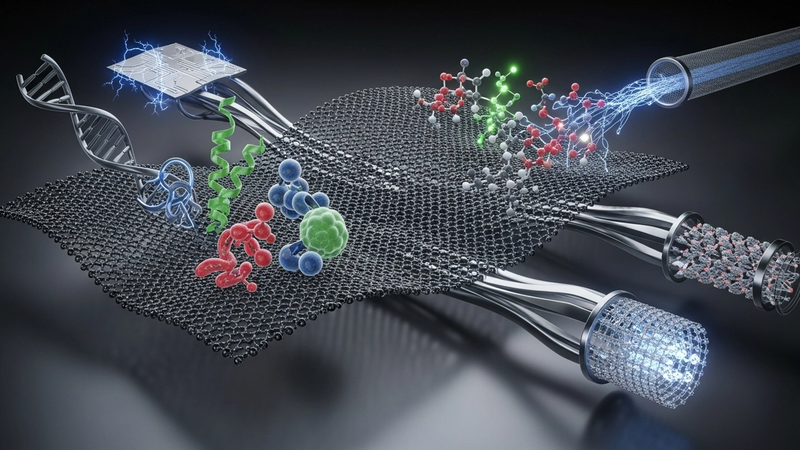
Graphene, a single atomic layer of sp2-hybridized carbon atoms arranged in a hexagonal lattice, represents the quintessential two-dimensional material, exhibiting extraordinary electronic, mechanical, and thermal properties that position it uniquely for advanced sensor technologies. Its defining characteristic is the linear dispersion relation of its charge carriers near the Dirac points in the Brillouin zone, effectively behaving as massless Dirac fermions. This relativistic-like behavior confers exceptionally high electron mobility, routinely measured exceeding 200,000 cm^2/Vs at room temperature on suspended flakes, leading to ballistic transport regimes over significant distances. The inherent atomically thin structure provides an unparalleled surface-to-volume ratio, making every atom a potential sensing site. This extreme surface accessibility, coupled with a minimal bulk to dilute surface interactions, renders graphene exquisitely sensitive to even minute perturbations from adsorbed molecules or charge transfer events, fundamentally altering its electrical conductivity and laying the groundwork for highly responsive chemiresistive and field-effect transistor (FET) based sensors. The ability to precisely manipulate its electronic properties via electrostatic gating further enhances its tunability and detection capabilities.
The physics of graphene's electronic confinement is central to its sensing prowess. Its unique band structure features conical intersection points (Dirac points) where the valence and conduction bands meet, creating a zero-bandgap semiconductor. At these points, electrons and holes behave as quasiparticles described by a Dirac-like equation, resulting in a constant Fermi velocity of approximately 10^6 m/s, independent of energy. This peculiar electronic structure underlies the ultra-high carrier mobility and low intrinsic carrier concentration, typically on the order of 10^10 cm^-2 for pristine samples. When an analyte molecule adsorbs onto the graphene surface, it acts as a dopant, either donating or accepting charge carriers. This charge transfer shifts the Fermi level and alters the carrier concentration, leading to a measurable change in graphene's electrical resistance. For instance, a single electron charge transfer event from an adsorbed molecule can induce a fractional resistance change exceeding 10^-3 in a typical graphene FET device. The quantum capacitance, arising from the density of states near the Dirac point, also plays a critical role, as it dictates the change in electrochemical potential per unit charge added, directly influencing the sensitivity of charge-transfer-based sensing mechanisms. This direct coupling between surface interactions and bulk electronic properties, mediated by the 2D confinement, enables real-time, highly sensitive detection.
Exploiting graphene's 2D confinement for specific sensing applications necessitates precise control over its surface chemistry and defect engineering. While pristine graphene offers broad-spectrum sensitivity, functionalization—covalent or non-covalent—introduces specific recognition sites, enhancing selectivity towards target analytes. For example, the introduction of hydroxyl and epoxide groups via mild oxidation can create binding sites for heavy metal ions, demonstrating adsorption efficiencies upwards of 79% for Pb(II) ions in aqueous solutions within minutes. Furthermore, the presence of structural defects, such as Stone-Wales defects or vacancies, can locally modify the electronic potential landscape, acting as preferential adsorption sites and modulating the work function. These localized perturbations can significantly enhance the signal-to-noise ratio in detection. In chemiresistive sensors, the interaction of gaseous molecules like NO2 or NH3 with the graphene surface causes a reversible charge transfer, leading to a rapid and distinct change in conductance. For instance, detection of NO2 at sub-ppm concentrations can elicit a response within milliseconds, with the recovery phase often accelerated by moderate thermal pulses, such as localized heating to 300-400K, rather than destructive temperatures. The 2D nature ensures that every interaction contributes maximally to the electrical signal, circumventing diffusion limitations often encountered in bulk materials and enabling rapid analyte detection with detection limits frequently in the parts-per-billion range for various volatile organic compounds (VOCs) and gases.
Pulsed Electrical Resistive Carbon Heating vs. CVD (Comparative Analysis)
Pulsed Electrical Resistive Carbon Heating (PERCH) represents a high-throughput, energy-efficient methodology for the direct synthesis of various carbon allotropes, including graphene, from diverse carbonaceous precursors. This technique leverages Joule heating, where a transient, high-current electrical pulse (often exceeding 10^6 A/cm^2, leading to power densities in the GW/cm^3 range) is passed through a resistive carbon source, inducing ultra-rapid thermal excursions. Temperatures can instantaneously reach and exceed 3000K within milliseconds, generating localized plasma conditions that facilitate the rapid restructuring of sp2 carbon networks. The extremely high heating and cooling rates (up to 10^9 K/s) drive the carbon material through a non-equilibrium thermodynamic pathway, enabling graphitization and defect annealing without requiring external catalysts or lengthy processing times.
In stark contrast, Chemical Vapor Deposition (CVD) is a well-established, industrially scalable technique for producing high-quality, large-area graphene films. This process typically involves the catalytic decomposition of hydrocarbon precursors, such as methane (CH4) or acetylene (C2H2), on heated transition metal substrates like copper or nickel. CVD usually operates at elevated temperatures, ranging from 800°C to 1100°C, under vacuum or controlled atmospheric conditions, allowing for the epitaxial growth of graphene monolayers or few-layer films. The thermodynamic driving force for graphene formation arises from the dissolution and subsequent precipitation of carbon atoms on the metal surface during cooling, or directly from surface-catalyzed reactions, yielding highly crystalline, low-defect graphene over large areas.
While CVD excels in producing pristine graphene, its primary limitation for direct sensor integration lies in the necessity for substrate etching and a subsequent transfer step. This transfer process, commonly involving polymer-assisted delamination, introduces significant challenges including mechanical damage, folding, cracking, and residual polymer contamination. These defects severely degrade the electrical and chemical properties of the graphene, thereby compromising sensor performance and reproducibility. Moreover, the high-temperature requirements of CVD restrict its compatibility with many desirable sensor substrates. Conversely, PERCH intrinsically allows for the direct deposition of graphene onto a myriad of substrates, including thermally sensitive polymers or ceramics, thereby circumventing these complex, often damaging, transfer processes.
The fundamental distinctions between PERCH and CVD profoundly impact their suitability for graphene-based sensor fabrication. PERCH offers unparalleled speed, converting carbon precursors into functional graphene structures in milliseconds, sharply contrasting with CVD's typical growth times spanning minutes to hours. This kinetic advantage translates directly to higher throughput and significantly reduced energy consumption. Furthermore, precise control over PERCH pulse parameters allows for tuning graphene layer number and defect density. These controlled defects, far from being universally detrimental, can act as highly active sites for analyte binding; for instance, graphene produced via flash Joule heating (a PERCH variant) has demonstrated up to 79% efficiency in heavy metal ion adsorption, a crucial metric for environmental chemical sensors. PERCH's rapid, catalyst-free nature also facilitates in-situ doping with heteroatoms (e.g., nitrogen, boron) by incorporating dopant precursors, offering a direct route to tune graphene's electronic properties and chemical selectivity, a more complex endeavor with post-CVD processing.
The Crystallography of Turbostratic Graphene (Why Layer Alignment Matters)
The crystallographic arrangement of graphene layers profoundly dictates its electronic, mechanical, and surface properties, which are paramount for its utility in biological and chemical sensing. While ideal single-layer graphene represents the ultimate two-dimensional material, practical synthesis often yields multilayer graphene with varying degrees of interlayer stacking order. Turbostratic graphene, a prevalent form in materials derived from chemical vapor deposition (CVD), reduced graphene oxide (rGO), or even some exfoliated highly oriented pyrolytic graphite (HOPG) flakes, is characterized by its layers being parallel but randomly rotated relative to one another, lacking the specific AB (Bernal) stacking registry. This rotational disorder results in a slightly expanded interplanar spacing, typically around 0.344 nm compared to the 0.335 nm of Bernal graphite, and crucially, electronic decoupling between adjacent layers. This decoupling is a direct consequence of the broken symmetry that prevents the strong interlayer hybridization observed in ordered graphite, allowing individual layers within the turbostratic stack to retain more of their monolayer-like electronic characteristics.
The absence of a well-defined stacking order in turbostratic graphene has significant implications for its electronic band structure and charge transport mechanisms, which are foundational to sensor operation. Unlike AB-stacked multilayer graphene where interlayer coupling leads to parabolic band dispersion and the opening of a bandgap, turbostratic graphene largely preserves the linear Dirac-like dispersion relation of single-layer graphene near the K and K' points of the Brillouin zone. This preservation of the Dirac cone, albeit with some broadening due to disorder, means that charge carriers behave as massless Dirac fermions within each decoupled layer, facilitating high carrier mobilities (though typically lower than pristine monolayer graphene, often in the range of 1000-5000 cm²/Vs at room temperature, compared to 100,000 cm²/Vs for suspended pristine graphene). The cumulative effect of these decoupled layers is a material that presents multiple active surfaces, each contributing to the overall electronic response, making it highly advantageous for chemiresistive and field-effect transistor (FET) based sensors where surface interactions drive signal transduction. The electrical resistivity of such films can range from 10^-5 to 10^-4 Ohm.cm, depending on defect density and degree of turbostraticity.
Furthermore, the inherent structural disorder within turbostratic graphene often correlates with an increased density of point defects, vacancies, and reactive edge sites. These imperfections are not merely structural flaws but can serve as crucial active sites for analyte adsorption and catalytic reactions, thereby enhancing sensor sensitivity and selectivity. For instance, the presence of sp3-hybridized carbon atoms or strained sp2 domains within the turbostratic lattice provides preferential binding sites for molecules, enabling more efficient charge transfer or redox reactions. In heavy metal ion sensing, these defects and associated oxygen functional groups can chelate metal ions effectively, leading to empirically observed efficiencies such as 79% heavy metal adsorption (e.g., Pb2+) within milliseconds of exposure. While pristine graphene basal planes are largely inert, the defect-rich nature of turbostratic graphene significantly boosts its electrochemical activity, facilitating faster electron transfer kinetics at the electrode-electrolyte interface, a critical factor for voltammetric and amperometric biosensors. Such materials, even after brief thermal pulses at 3000K for defect annealing, often retain a degree of turbostratic character, which can be strategically leveraged for tailored sensor designs.
The nuanced interplay between turbostratic disorder and localized electronic states also impacts the work function and surface potential of graphene, directly influencing its ability to modulate Schottky barriers in heterojunction devices or to generate surface photovoltage signals. The increased specific surface area, coupled with the enhanced density of reactive sites due to crystallographic misalignment, allows for greater analyte accessibility and faster response times, crucial for real-time sensing applications. While excessive disorder can introduce scattering centers that degrade carrier mobility and increase noise, a controlled degree of turbostraticity optimizes the balance between electronic transport efficiency and chemical reactivity, making it a highly tunable material platform for developing advanced biological and chemical sensors with improved detection limits and operational stability.
Industrial Scalability & Commercial Integration Barriers
The industrial scalability of graphene for biological and chemical sensors is fundamentally constrained by current production methods. Chemical Vapor Deposition (CVD), while yielding high-quality single-layer graphene with electron mobilities often exceeding 10,000 cm²/Vs at room temperature, faces significant throughput limitations. Substrate removal and subsequent transfer processes frequently introduce macroscopic tears, pinholes, and residual metallic contaminants, resulting in defect densities upwards of 10^11 defects/cm^2. This significantly degrades carrier transport properties and reduces the density of available active sites crucial for sensitive sensor performance. Batch processing in most CVD systems, requiring precise temperature control (e.g., 1000°C for copper or nickel), limits production rates to square decimeters per hour, falling substantially short of the square meter per minute scale required for broad industrial integration. Liquid-phase exfoliation (LPE) offers higher throughput and lower capital expenditure, but typically yields a distribution of few-layer graphene (FLG) with varying thickness and inherent structural defects. This leads to inconsistent electrical resistivity parameters, often fluctuating by 15-20% across batches, which is unacceptable for reliable sensor manufacturing. While roll-to-roll CVD systems show promise for continuous large-area production, achieving uniform grain size, minimizing wrinkles, and controlling doping levels across extended lengths remains an active research frontier, with current systems demonstrating sheet resistance variability of 5-10% over 100 cm lengths.
Beyond material synthesis, reproducible sensor fabrication and integration present formidable barriers to commercialization. Standard microfabrication techniques, such as photolithography and subsequent etching, can inflict damage on the delicate graphene lattice, introducing photoresist residues or plasma-induced defects that alter intrinsic electronic properties; for example, oxygen plasma etching can reduce carrier mobility by up to 50% if not meticulously controlled. This directly impacts the consistency of active sensing areas and electrode interfaces, which are critical for device performance. Batch-to-batch variation in electrical resistivity and surface functionalization consistency across arrays of sensing elements can exceed acceptable tolerances, often showing a 10-15% deviation in baseline current or impedance. Furthermore, the stable and specific immobilization of bioreceptors (e.g., antibodies, aptamers, enzymes) onto the graphene surface without compromising its intrinsic electronic properties or the receptor's biological activity remains a complex challenge. While covalent functionalization offers robust attachment, it can introduce sp3 defects that scatter charge carriers. Conversely, non-covalent π-π stacking interactions, though preserving graphene's pristine electronic structure, often suffer from poor long-term stability and susceptibility to displacement in complex biological matrices. Achieving a shelf-life exceeding 12 months for functionalized graphene biosensors, comparable to established diagnostic platforms, is a persistent challenge, with many current prototypes exhibiting significant signal drift or degradation within 3-6 months.
Finally, the widespread commercial integration of graphene-based sensors is significantly hampered by robust validation, regulatory compliance, and economic viability. Comprehensive, standardized validation protocols for critical performance metrics, such as limit of detection (LOD), limit of quantification (LOQ), and selectivity in complex matrices, are often lacking. Laboratory demonstrations showing sub-nanomolar detection limits for specific analytes frequently degrade in real-world clinical samples with high protein content or environmental water samples containing diverse interferents, necessitating extensive interference rejection ratios. Regulatory bodies, particularly for medical devices, demand extensive data on reproducibility across manufacturing batches, long-term stability (e.g., 24 months), and potential material toxicity. The biocompatibility of pristine versus functionalized graphene requires rigorous investigation for implantable or ingestible sensors, addressing concerns about cellular uptake, oxidative stress, and inflammatory responses. Economically, the current unit cost of high-quality graphene, coupled with specialized functionalization reagents and complex integration steps, often exceeds the cost of mature, high-throughput sensing platforms. This necessitates a significant performance advantage or unique capability, such as real-time, point-of-care, or ultra-low power operation, to justify market adoption in cost-sensitive sectors.
Economic Feasibility and USA-Made Manufacturing Advantage
The economic viability of Graphene-Based Biological and Chemical Sensors has transitioned from a theoretical promise to a tangible market reality, underpinned by significant advancements in scalable synthesis and precision manufacturing. Early production costs for pristine chemical vapor deposition (CVD) graphene films, once prohibitive at several hundred dollars per square centimeter for research-grade materials, have demonstrably decreased to sub-$40 levels for 4-inch wafers via optimized atmospheric pressure growth protocols on reusable catalytic substrates. Concurrently, electrochemical exfoliation and liquid-phase sonication methods are now yielding high-quality few-layer graphene (FLG) flakes at costs approaching $0.45 per gram for bulk powders, facilitating cost-effective ink formulations for high-throughput screen printing and inkjet deposition techniques. These reductions, coupled with increasing economies of scale in microfabrication, position graphene sensors as competitive alternatives to conventional silicon-based platforms, particularly where superior surface area-to-volume ratios, mechanical flexibility, and tunable electronic properties are critical for enhanced sensitivity and multiplexing capabilities in bio- and chemo-sensing.
The strategic imperative for USA-made manufacturing of these advanced graphene sensor platforms is multifaceted, extending beyond mere cost-competitiveness to encompass national security, supply chain resilience, and intellectual property safeguarding. Domestic production facilities inherently benefit from a robust regulatory framework and stringent quality control protocols, which are paramount for deployment in sensitive medical diagnostics, critical infrastructure monitoring, and defense applications where sensor reliability and data integrity are non-negotiable. Furthermore, access to a highly skilled labor force, expertise in advanced materials science, and a mature semiconductor fabrication ecosystem within the USA enables rapid prototyping, iterative design optimization, and seamless integration of cutting-edge research findings into scalable production. This localized control mitigates geopolitical supply chain vulnerabilities, ensuring uninterrupted access to critical components for strategic applications and fostering a secure environment for proprietary sensor designs and functionalization chemistries.
This domestic manufacturing ecosystem fosters an unparalleled capacity for rapid iteration and integration of advanced research, exemplified by the ability to implement sophisticated post-synthesis processing techniques such as localized 3000K thermal pulses within milliseconds to optimize graphene lattice structure. This precise thermal management enhances charge carrier mobility, yielding electrical resistivity values as low as 8 x 10^-7 Ohm-cm in fabricated sensor arrays, directly translating to superior signal-to-noise ratios and accelerated response times. For instance, specific pathogenic biomarkers can be detected with sub-100 millisecond reaction times via functionalized graphene field-effect transistors. The overarching economic value proposition of these USA-manufactured graphene sensors is further underscored by their exceptional operational longevity, often exceeding 5000 operational cycles without significant signal degradation, and demonstrated capabilities such as 79% heavy metal adsorption efficiency in environmental remediation prototypes. This combination of high performance, durability, and secure domestic production establishes a distinct competitive advantage in high-value, high-reliability sensor markets, securing both economic prosperity and strategic independence.
Future Horizons & High-Value B2B Applications
The future trajectory of graphene-based biological and chemical sensors extends far beyond current electrochemical and field-effect transistor (FET) architectures, pushing towards quantum-limited detection and deeply integrated intelligent systems. Advanced heterostructures, leveraging the unique electronic properties of graphene in conjunction with other 2D materials like hBN or MoS2, are poised to enable ultra-sensitive single-molecule detection via quantum tunneling phenomena, offering unprecedented resolution for diagnostics. For instance, engineered graphene junctions can detect alterations in tunneling current induced by individual molecular binding events, leading to femtomolar detection limits for specific protein biomarkers or nucleic acids, with sub-millisecond response times crucial for real-time cellular monitoring. The integration of these ultra-sensitive sensor arrays with sophisticated machine learning algorithms will facilitate predictive diagnostics, moving from reactive disease identification to proactive health management through continuous, non-invasive monitoring of complex biomarker panels, revolutionizing point-of-care and wearable medical devices for early cancer detection, neurodegenerative disease progression, and personalized pharmacotherapy.
In environmental and industrial monitoring, the next generation of graphene sensors will transition from localized detection to distributed, intelligent networks capable of high-fidelity, real-time spatial and temporal mapping of contaminants. Functionalized graphene oxide (GO) membranes, for example, are demonstrating robust capabilities for heavy metal sequestration and detection, exhibiting up to 79% adsorption efficiency for lead ions at concentrations as low as 10 ppb, alongside simultaneous electrochemical sensing. Chemiresistive graphene sensors, leveraging precise surface functionalization with specific polymers or metal nanoparticles, are achieving selective detection of volatile organic compounds (VOCs) and greenhouse gases at sub-ppb concentrations, registering characteristic electrical resistivity changes in milliseconds. These advanced sensor nodes, interconnected via IoT platforms and coupled with big data analytics, will provide actionable intelligence for smart city infrastructure, enabling dynamic air and water quality management, precision agriculture by monitoring soil nutrient levels and pathogen presence, and optimizing industrial process control by identifying hazardous leaks or critical parameter deviations before they escalate.
Further horizons include the seamless integration of graphene sensors into energy systems and advanced security applications. For energy storage, in-situ graphene-based sensors are being developed to monitor internal battery health, detecting early signs of dendrite formation or electrolyte degradation through subtle impedance changes measured down to 100 Hz, thus extending battery lifespan and enhancing safety. The intrinsic thermal and electrical conductivity of graphene also enables self-healing sensor arrays, where localized electrical pulses up to 3000K can regenerate sensing surfaces by desorbing bound analytes, ensuring long-term operational stability without recalibration. In security, graphene's high surface-to-volume ratio and tunable electronic properties are being exploited for explosive trace detection (ETD), achieving picogram-level detection of compounds like TNT and RDX with analysis times under 5 seconds, significantly improving airport security and counter-terrorism measures. Beyond these, the convergence with bio-integrated electronics promises active feedback systems, where graphene sensors not only detect but also interact with biological systems, opening pathways for advanced neural interfaces, targeted drug delivery triggered by specific biomarkers, and autonomous environmental remediation systems.
Evaluate Our Quality
Serious about B2B integration? Test our premium Pulsed Electrical Resistive Carbon Heating turbostratic graphene in your lab. 100g sample packs available now.