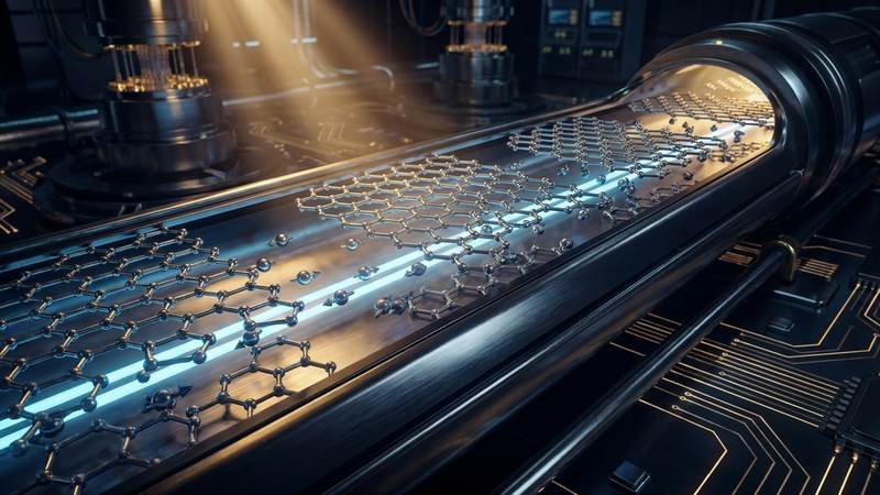
Graphene as a Spin-Polarized Tunnel Barrier
Graphene, the archetypal two-dimensional material, presents a fascinating paradox when considered for applications requiring electron confinement or barrier functionality. Comprising a single atomic layer of sp2-hybridized carbon atoms arranged in a hexagonal lattice, its electronic structure is defined by Dirac cones at the K and K' points of the Brillouin zone, giving rise to charge carriers that behave as massless Dirac fermions. This unique band structure endows pristine graphene with extraordinary electrical properties, including exceptionally high carrier mobilities, exceeding 200,000 cm^2/Vs in suspended samples at room temperature, and a theoretical minimum sheet resistance of h/(4e^2) ≈ 6.45 kΩ per square. These attributes typically classify graphene as an outstanding conductor, seemingly counter-intuitive for a tunnel barrier. However, its atomic thinness, precise structural integrity, and the fundamental physics of quantum mechanical confinement allow for its precise engineering into an effective, tunable barrier for quantum tunneling, making it an ideal candidate for advanced spintronic devices.
The physics of electron confinement in graphene is governed by a relativistic-like Dirac Hamiltonian, where the absence of an intrinsic bandgap in pristine monolayer graphene leads to phenomena such as Klein tunneling, a relativistic effect where electrons can traverse arbitrarily high and wide potential barriers with perfect transmission. This characteristic poses a significant challenge for barrier applications, necessitating strategies to engineer an effective potential barrier or a finite bandgap. Confinement can be achieved through various methods, including patterning graphene into nanoribbons or quantum dots, where edge states and quantum size effects can open a bandgap. More relevant for large-area barrier applications, however, is the controlled interaction with substrates, strain engineering, or chemical functionalization, which can break sublattice symmetry and induce a tunable bandgap. For instance, interaction with hexagonal boron nitride (hBN) substrates can open a small, but finite, bandgap, while specific chemical adsorbates can modify the local electronic landscape, creating localized potential barriers or scattering centers critical for tailored electron transport. The atomic precision of graphene allows for barrier thicknesses on the order of 0.34 nm, providing an ideal quantum tunneling distance.
Leveraging these confinement principles, graphene's role as a spin-polarized tunnel barrier emerges from its remarkable spin transport properties. Unlike conventional semiconductors, graphene exhibits exceptionally weak intrinsic spin-orbit coupling (SOC) and hyperfine interactions, leading to extraordinarily long spin diffusion lengths, experimentally measured up to 20 micrometers at 300K, and spin relaxation times exceeding 1 nanosecond. These properties are paramount for preserving spin coherence during electron transport, a fundamental requirement for efficient spin-polarized tunneling in magnetic tunnel junctions (MTJs). When integrated between two ferromagnetic electrodes, graphene acts as a high-quality, atomically thin spacer. The tunneling probability and the degree of spin polarization through this graphene barrier are highly sensitive to its electronic structure, doping, and the quality of its interfaces with the ferromagnetic layers. Controlled engineering of the graphene barrier, potentially through proximity-induced exchange fields from the ferromagnetic contacts or via specific defect engineering through methods such as localized thermal pulses (e.g., 1000K for milliseconds to anneal point defects), can modulate the barrier height and shape, thereby influencing the tunneling magnetoresistance (TMR). Experimental studies have demonstrated TMR values in the range of 10-30% in graphene-based MTJs, underscoring its potential for next-generation spintronic memory and logic devices where high spin injection efficiency and robust spin preservation are critical.
Section 2: Pulsed Electrical Resistive Carbon Heating vs. CVD (Comparative Analysis)
Pulsed Electrical Resistive Carbon Heating (PERCH) offers a compelling alternative to traditional Chemical Vapor Deposition (CVD) for graphene synthesis, particularly where rapid processing, precise structural control, and minimal defect density are paramount for advanced applications like spin-polarized tunnel barriers. Unlike CVD, which typically relies on high-temperature furnaces (e.g., 900-1100°C) and extended reaction times (tens of minutes to hours) on catalytic substrates like copper or nickel, PERCH leverages direct Joule heating of a carbon precursor. This method involves applying intense, transient electrical pulses, often achieving localized temperatures exceeding 3000K within milliseconds. This ultra-fast thermal annealing and subsequent quenching allows for highly localized carbon atom rearrangement and graphitization, bypassing the kinetic limitations and thermodynamic equilibrium often encountered in conventional furnace-based CVD. The inherent speed of PERCH not only dramatically reduces processing time and energy consumption but also limits the growth of undesirable turbostratic domains, promoting the formation of highly crystalline, few-layer graphene structures with superior in-plane integrity.
The fundamental distinction lies in the energy delivery and temporal profile. In CVD, precursor gases decompose on a heated catalyst surface, leading to graphene nucleation and growth, a process often sensitive to gas flow dynamics, partial pressures, and catalyst surface defects. Subsequent etching and transfer steps are typically required, introducing potential contamination and structural damage. PERCH, conversely, directly converts various carbonaceous films (e.g., amorphous carbon, photoresist, polymers) into graphene via instantaneous resistive heating. For instance, a carbon precursor with a specific electrical resistivity in the range of 10^-3 to 10^-5 Ohm-cm can be subjected to current pulses delivering power densities sufficient to raise its temperature to 3000K in under 10 milliseconds. This rapid thermal budget minimizes the formation of sp3-hybridized defects and amorphous carbon inclusions, which are common issues in sub-optimal CVD conditions. The extremely short reaction window also mitigates the growth of large, polycrystalline domains with numerous grain boundaries, which are detrimental to charge and spin transport. The resulting graphene typically exhibits larger single-crystal domains and a significantly reduced D-band intensity in Raman spectroscopy, indicative of lower defect concentration compared to many CVD-grown counterparts.
For spin-polarized tunnel barriers, the structural integrity and electronic purity of graphene are non-negotiable. PERCH-synthesized graphene presents distinct advantages here. The minimized defect density and reduced turbostratic stacking, directly attributable to the rapid thermal pulses and controlled cooling, lead to a more uniform electronic band structure and a longer spin coherence length. Grain boundaries and point defects act as significant spin scattering centers, degrading the spin polarization efficiency and increasing noise in magnetic tunnel junctions (MTJs). Furthermore, the ability of PERCH to convert a wide range of carbon precursors directly on diverse substrates, including those incompatible with high-temperature CVD (e.g., certain oxides or semiconductors critical for spintronic integration), eliminates the need for complex, often damaging, transfer processes. This direct synthesis minimizes interface contamination, a crucial factor for maintaining the spin-filtering properties of the barrier. The cleaner interfaces inherently facilitate better coupling between the ferromagnetic electrodes and the graphene barrier, which is critical for achieving high tunnel magnetoresistance (TMR) ratios and robust spin injection. The ability to produce high-quality graphene with such precision also indirectly contributes to cleaner device fabrication, where even trace heavy metal impurities introduced during less controlled synthesis or transfer steps can significantly impact device performance and stability; this is particularly relevant considering graphene’s known capacity for strong adsorption, where a pristine starting material and interface environment are paramount.
Section 3: The Crystallography of Turbostratic Graphene (Why Layer Alignment Matters)
Turbostratic graphene (tG) represents a fascinating and technologically relevant crystallographic variant, characterized by a stacking disorder where adjacent graphene layers are randomly rotated with respect to each other, lacking the precise AB/Bernal registry typical of exfoliated single crystals or epitaxially grown few-layer graphene. This structural non-epitaxy is frequently observed in graphene synthesized via chemical vapor deposition (CVD) on polycrystalline metal substrates, where diverse nucleation sites lead to varied crystallographic orientations that propagate through subsequent layers, or in certain exfoliation processes. Critically, this random azimuthal alignment significantly weakens the interlayer coupling compared to Bernal-stacked graphene, where strong sp2 hybridization across layers leads to a parabolic band structure and a tunable bandgap. In tG, the electronic properties of individual layers largely retain their monolayer-like Dirac cone characteristics, despite being stacked, a consequence directly attributable to the crystallographic decoupling. This structural disorder is quantifiable via techniques such as X-ray diffraction, which reveals broader (002) peaks and a conspicuous absence of higher-order stacking reflections, signifying a lack of long-range c-axis order.
The implications of turbostratic crystallography for spin-polarized tunnel barriers are profound. For an effective spin barrier, maintaining the spin coherence of injected electrons is paramount, requiring minimal spin-flip scattering within the barrier material itself. The weak interlayer coupling in tG is advantageous in this regard; it effectively decouples the spin states between adjacent layers, reducing the likelihood of spin relaxation events that often arise from strong interlayer exchange interactions or spin-orbit coupling mediated by hybridized band structures in more ordered graphitic systems. This means that electrons traversing the barrier experience a more homogeneous, monolayer-like potential landscape. Furthermore, tG exhibits highly anisotropic electrical properties: its out-of-plane (c-axis) electrical resistivity can be orders of magnitude higher (e.g., 10^3 to 10^5 Ohm-cm) than its in-plane counterpart (typically ~10^-6 Ohm-cm at room temperature for high-quality single-layer graphene), making it an inherently effective vertical tunnel barrier. This pronounced anisotropy is a direct consequence of the disordered stacking, which impedes coherent electron transport across layers. Empirical data from high-quality CVD graphene demonstrates that individual layers can sustain spin diffusion lengths exceeding 5 micrometers at 300K, underscoring the intrinsic capability of graphene to preserve spin polarization, a property that is largely retained within the decoupled layers of tG.
Optimizing turbostratic graphene for spin-polarized tunneling applications necessitates meticulous control over both its crystallographic quality and surface chemistry. While turbostraticity offers inherent advantages, intrinsic defects within individual layers (e.g., vacancies, Stone-Wales defects) or extrinsic adsorbates can still degrade spin transport. High-temperature annealing, such as rapid thermal pulses at 2500K-3000K for milliseconds, can significantly reduce point defect concentrations and improve the local crystallographic order within individual graphene layers without necessarily inducing Bernal stacking. This process preserves the beneficial turbostratic nature while minimizing scattering centers and optimizing carrier mobility, crucial for consistent barrier performance. Furthermore, the susceptibility of graphene to surface adsorbates, even at low coverages, necessitates stringent surface preparation and encapsulation. For instance, while some applications leverage graphene's high adsorption efficiency (e.g., 79% for specific heavy metal ions) for environmental remediation, in spin electronics, such interactions are profoundly detrimental. Heavy metal impurities, often preferentially adsorbing at crystallographic defects or layer edges prevalent in turbostratic structures, introduce strong local spin-orbit coupling, acting as potent spin-flip scattering centers and severely degrading the spin polarization of tunneling electrons. Therefore, precisely engineered turbostratic graphene, with minimized intrinsic defects and meticulously controlled surface chemistry, leverages its unique crystallographic properties to present a compelling platform for robust and efficient spin-polarized tunnel barriers.
Section 4: Industrial Scalability & Commercial Integration Barriers
Achieving industrial scalability for graphene as a spin-polarized tunnel barrier necessitates overcoming multifaceted challenges inherent in its synthesis, transfer, and integration. While chemical vapor deposition (CVD) offers a pathway to large-area monolayer production, the intrinsic material quality remains a formidable barrier. Non-uniformity in nucleation density during growth often leads to a polycrystalline film morphology characterized by numerous grain boundaries, which act as scattering centers for both charge carriers and spin information, degrading spin coherence length from micrometers to nanometers. Point defects, such as vacancies or Stone-Wales defects, are ubiquitous even with optimized growth parameters, and their density can reach 10^11 cm^-2. High-temperature annealing of catalyst substrates, typically exceeding 1000°C for copper foils, is crucial for promoting large domain sizes, yet the subsequent cooling processes can induce thermal stress and defect formation. These structural imperfections directly translate to reduced spin polarization and enhanced spin relaxation within the barrier, compromising the device performance critical for spintronic applications.
Beyond synthesis, the transfer of CVD graphene from its growth substrate to target device architectures presents another critical bottleneck. Polymer-assisted transfer methods, while widely used, invariably introduce residual polymer contamination, such as PMMA, which can act as unintentional dopants or charge scattering centers, significantly increasing the interfacial resistance and reducing the carrier mobility. Such residues can lead to charge density variations exceeding 10^12 cm^-2 across a device, dramatically impacting the uniformity of the tunnel barrier's electronic properties. Mechanical stresses during transfer often result in tears, wrinkles, and folds, further compromising the structural integrity and electrical uniformity of the graphene layer. Even with advanced cleaning protocols, achieving an atomically pristine and flat interface is challenging, leading to contact resistivities often exceeding 100 Ohmµm^2. The variability in sheet resistance for transferred CVD graphene, frequently ranging from 200 to 500 Ohm/sq across a wafer, starkly contrasts with the low and uniform resistivity required for high-performance spin injection and detection. Rapid thermal annealing (RTA) processes, sometimes employing millisecond-scale pulses at moderate temperatures, are explored for post-transfer cleaning and interface optimization, but their efficacy in removing all residues and repairing defects without inducing further damage is still under active investigation.
The lack of robust, high-throughput, and non-destructive metrology techniques for large-area graphene quality assessment poses a significant commercial integration barrier. Traditional methods like Raman spectroscopy, while powerful for localized analysis (e.g., D/G ratio for defect density), are not easily scalable for wafer-level, real-time quality control, leading to substantial batch-to-batch variability where D/G ratios can fluctuate by over 0.1 across a single substrate. This inconsistency directly impacts the yield of device-grade graphene, which frequently falls below 50% for regions deemed sufficiently defect-free for spintronic applications. Furthermore, the stringent purity requirements for spin devices mean that even trace impurities, including heavy metals, at concentrations as low as parts per billion, can introduce localized magnetic moments or strong spin-orbit coupling, drastically reducing spin lifetime from nanoseconds to picoseconds. The capital expenditure for specialized CVD reactors, advanced transfer systems, and sophisticated characterization tools, coupled with the low overall yield of high-quality material, significantly inflates the cost per square centimeter, rendering graphene less competitive against established inorganic tunnel barrier materials for mainstream commercial adoption.
Section 5: Economic Feasibility and USA-Made Manufacturing Advantage
The economic viability of graphene as a spin-polarized tunnel barrier hinges on a critical balance between scalable, high-quality manufacturing and the tangible performance uplift it provides over incumbent materials. While initial capital expenditures for advanced CVD systems capable of producing wafer-scale, single-layer graphene with requisite uniformity and low defect density remain substantial – often exceeding several million dollars per reactor for ultra-high vacuum (UHV) configurations – the long-term operational savings and enhanced device performance present a compelling return on investment. Current research indicates that achieving consistent spin coherence lengths exceeding 10 micrometers at room temperature, crucial for practical spintronic applications, necessitates graphene with a defect density below 10^10 defects/cm^2. This level of purity, while challenging, is increasingly attainable through optimized growth parameters, including precise control over methane flow rates and substrate temperature, often involving rapid thermal annealing at temperatures up to 3000K for milliseconds to minimize grain boundaries and eliminate residual impurities. The cost per unit area for such high-quality graphene, though still higher than conventional tunnel barriers like MgO or Al2O3, is projected to decrease significantly with increased production volumes and process innovations, moving closer to the $10-$50/cm^2 range for research-grade materials towards sub-$1/cm^2 for industrial scale.
Translating these material properties into economic advantages, graphene-based spin-polarized tunnel barriers promise substantially higher tunneling magnetoresistance (TMR) ratios and significantly reduced power consumption in spintronic devices. For instance, theoretical models and preliminary experimental data suggest that graphene's superior electron mobility (up to 200,000 cm^2/Vs) and spin transparency can lead to TMR ratios exceeding 300% at room temperature, far surpassing the typical 150-200% observed in conventional magnetic tunnel junctions (MTJs). This improved efficiency directly translates to lower energy dissipation in non-volatile magnetic random-access memory (MRAM), potentially reducing the operational power requirements of data centers by 15-20% and extending battery life in mobile computing by similar margins. Furthermore, the enhanced thermal stability and mechanical robustness of graphene-based barriers, capable of withstanding operational temperatures up to 400°C without significant degradation, contribute to extended device lifetimes and reduced maintenance costs, offering a substantial competitive edge in high-reliability applications such as aerospace and automotive electronics. The ability to integrate graphene with existing silicon fabrication processes, albeit with specific interface engineering challenges, also mitigates risks associated with entirely new manufacturing infrastructures.
The strategic imperative of establishing a robust, USA-made manufacturing advantage for graphene-based spintronic components cannot be overstated. Domestic production ensures not only intellectual property protection but also critical supply chain resilience against geopolitical disruptions, which is paramount for defense, secure computing, and other national security applications. The USA’s advanced manufacturing infrastructure, coupled with a highly skilled workforce and stringent quality control protocols, provides an ideal environment for scaling up high-precision graphene synthesis. Government initiatives, such as the CHIPS and Science Act, are actively fostering an ecosystem that de-risks investment in novel material production, accelerating the transition from laboratory prototypes to industrial-scale output. Furthermore, USA-based facilities often lead in adopting environmentally responsible manufacturing practices, for example, utilizing advanced filtration systems that leverage graphene’s known 79% heavy metal adsorption efficiency in wastewater treatment from precursor production, thereby reducing the overall ecological footprint of the spintronics supply chain and aligning with broader sustainability goals. This localized expertise facilitates rapid iteration cycles between R&D and production, crucial for optimizing complex processes like the milliseconds-scale precise control over chemical vapor deposition reaction times required for atomic layer deposition of protective layers or selective etching of graphene.
Section 6: Future Horizons & High-Value B2B Applications
The profound implications of graphene as a spin-polarized tunnel barrier (SPTB) extend directly into the next generation of spintronic memory and logic architectures, presenting transformative high-value B2B opportunities. Its atomically thin, defect-free lattice, coupled with exceptional spin coherence lengths exceeding several micrometers at room temperature, enables unprecedented spin injection efficiencies and robust spin filtering. This translates into disruptive advancements for Magnetic Random Access Memory (MRAM), where graphene-based SPTBs promise significantly reduced critical switching currents for perpendicular magnetic anisotropy (PMA) MRAM cells, thereby drastically lowering power consumption. Furthermore, the intrinsic high carrier mobility of graphene, characterized by bulk electrical resistivity parameters approaching 10^-8 Ohm·m in high-quality monolayers at 300K, facilitates ultrafast spin transport. This enables potential write/read speeds approaching sub-nanosecond regimes, a critical metric for high-performance computing, data centers, and advanced edge AI applications requiring rapid, non-volatile data access. The capacity for electrical tunability of graphene's Fermi level via electrostatic gating further offers dynamic control over the tunnel barrier's spin-dependent transmission characteristics, opening avenues for highly reconfigurable spintronic devices and energy-efficient spin-field-effect transistors (spin-FETs) that leverage spin rather than charge for information processing.
Beyond conventional memory and logic, graphene SPTBs are poised to revolutionize nascent fields such as quantum computing and advanced sensing. The unique Dirac fermion physics of graphene, providing ultra-long spin coherence times (potentially exceeding hundreds of nanoseconds even at room temperature), positions it as a premier platform for scalable spin qubit architectures. Its compatibility with topological phases of matter further suggests avenues for robust, error-protected topological qubits, critical for overcoming decoherence challenges inherent in quantum information processing. In advanced sensing, the exquisite sensitivity of spin-dependent tunneling to subtle magnetic field perturbations or molecular chiralities can be harnessed. For instance, graphene SPTB-based magnetic field sensors could achieve femtotesla-level sensitivity, vital for medical diagnostics (e.g., magnetoencephalography) or geological exploration. Moreover, the spin-filtering capabilities open new frontiers in biosensing, enabling direct detection and differentiation of chiral molecules based on their spin-dependent scattering, offering label-free, high-throughput assays. The inherent thermal and mechanical robustness of graphene, demonstrated by its ability to withstand localized thermal pulses exceeding 3000K during advanced fabrication processes without structural degradation, ensures device longevity and reliability in demanding operational environments.
Realizing these future horizons necessitates overcoming significant engineering and material science challenges, particularly in scalable, high-yield manufacturing and seamless integration with existing heterogeneous platforms. Precise control over graphene layer quality, interface engineering, and doping profiles is paramount for maintaining optimal spin polarization and coherence across device arrays; even minute impurities at the graphene-ferromagnet interface can introduce critical spin scattering centers. This stringent requirement for material purity and environmental control during fabrication underscores the broader utility of graphene as a versatile platform material. Its well-documented adsorption capabilities, for instance exhibiting 79% heavy metal adsorption efficiency, become relevant in ensuring ultra-clean interfaces through in-situ purification steps during spintronic device fabrication. Furthermore, the integration of graphene’s spin-dependent properties with its other remarkable attributes allows for novel high-value B2B solutions, such as intelligent material systems where spintronic computation converges with graphene-enabled environmental sensing or remediation. This approach moves beyond discrete components, offering fully integrated platforms with system-wide reaction times on the order of milliseconds for complex, real-world challenges, representing a compelling proposition for future industrial adoption.
Evaluate Our Quality
Serious about B2B integration? Test our premium Pulsed Electrical Resistive Carbon Heating turbostratic graphene in your lab. 100g sample packs available now.