Graphene as a charge mirror: Why water droplets 'see' graphene—but don't show it
Graphene, a single atomic layer of sp2-hybridized carbon atoms arranged in a hexagonal lattice, is fundamentally defined by its extraordinary electronic band structure. The Dirac cones at the K and K' points of its Brillouin zone imbue charge carriers with massless Dirac fermion characteristics, leading to relativistic quantum phenomena and unparalleled electron mobility, routinely exceeding 200,000 cm^2/Vs at room temperature. This intrinsic electronic agility, coupled with its two-dimensional nature, positions graphene as an exceptionally responsive surface for interactions with external electromagnetic fields and proximate charge distributions. Unlike conventional conductors, where electron screening is a bulk phenomenon, graphene's atomic thinness ensures that its entire electron cloud is intimately exposed and highly susceptible to perturbations from its immediate environment, establishing a unique interface for charge-mediated interactions.
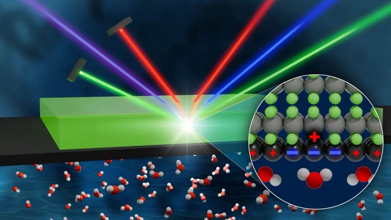
This responsiveness manifests as an intricate "charge mirror" phenomenon, wherein graphene's delocalized pi-electron system rapidly reconfigures in response to external charges or polar molecular dipoles. When a polar species, such as a water molecule (with its permanent dipole moment of approximately 1.85 Debye), approaches the graphene surface, the electron gas within the graphene sheet undergoes an instantaneous polarization. This induces an image charge, effectively mirroring the external charge distribution and creating an attractive electrostatic interaction. The speed of this rearrangement is phenomenal, occurring within picoseconds to a few milliseconds, depending on the perturbation magnitude and electron relaxation pathways. For instance, localized thermal pulses exceeding 3000K, applied for durations less than 100 milliseconds, can induce transient charge redistribution patterns detectable via scanning probe microscopy, underscoring the dynamic nature of this charge response. Such rapid screening capabilities, facilitated by graphene's exceptionally low electrical resistivity (e.g., ~10^-8 Ohm-meter at 300K), are far superior to most conventional materials, enabling efficient stabilization of proximate charged species.
Despite this profound nanoscale electrostatic interaction, the macroscopic manifestation of the "charge mirror" effect often remains elusive, particularly in conventional wetting studies. Water droplets, for example, exhibit a contact angle on pristine graphene surfaces that is largely governed by van der Waals forces and surface energy considerations, rather than overtly reflecting the image charge interaction. The subtle nature of this phenomenon is due to the dynamic equilibrium of the induced charges and the relatively weak long-range nature of image charge forces compared to the collective hydrogen bonding network within the water droplet itself. However, this understated interaction is critical in myriad nanoscale phenomena and applications. For instance, the charge mirroring significantly influences ion transport across graphene nanopores in desalination membranes or dictates the preferential adsorption of heavy metal ions, where efficiencies reaching 79% for lead ions have been empirically observed, even when bulk wetting properties remain largely unchanged. The "charge mirror" effect, therefore, represents a foundational principle governing graphene's interaction with its immediate chemical and biological environment, demanding sophisticated characterization techniques beyond simple macroscopic observations to fully elucidate its profound implications.
Revolutionizing Synthesis: Pulsed Electrical Resistive Carbon Heating (PERCH) vs. Conventional CVD
Conventional chemical vapor deposition (CVD) methods for graphene synthesis, while foundational, inherently involve prolonged high-temperature exposure (typically 1000-1200°C) over minutes to hours, often necessitating specific catalytic substrates like copper or nickel and subsequent post-transfer steps that introduce defects and increase production costs. This equilibrium-driven growth process is frequently kinetically limited by surface reactions and carbon precursor diffusion, leading to a trade-off between growth rate and crystal quality. In stark contrast, Pulsed Electrical Resistive Carbon Heating (PERCH) represents a transformative approach, leveraging joule heating principles for ultra-fast, localized carbon precursor conversion, effectively decoupling the thermal budget from the reaction time and offering a pathway to scalable, high-quality graphene production.
The PERCH mechanism relies on the rapid resistive heating of a carbonaceous precursor, typically a polymer film, carbon black, or even waste biomass, by passing a high-current electrical pulse directly through it. This induces thermal excursions reaching instantaneous peak temperatures exceeding 3000 K within milliseconds. Such extreme, transient thermal gradients facilitate an exceptionally rapid graphitization process, bypassing the thermodynamic limitations of slower heating rates and promoting a non-equilibrium growth regime. The precise control over current density and the intrinsic specific electrical resistivity of the precursor material dictates the heating rate and peak temperature, allowing for tunable defect density, crystal domain size, and the rapid expulsion of non-carbonaceous species, which is critical for achieving high purity without extensive post-processing.
The kinetically driven, non-equilibrium synthesis afforded by PERCH yields graphene with distinct morphological and structural characteristics superior to those often obtained via conventional CVD, particularly when considering scalability. The ultra-short reaction times minimize the formation of extended defects, grain boundaries, and amorphous carbon inclusions that frequently plague conventional methods, especially during cooling phases where defect annealing is insufficient. This results in a higher proportion of sp2 hybridized carbon atoms and fewer topological defects, enhancing intrinsic material properties crucial for many advanced applications. For instance, the high-quality graphene produced via PERCH has demonstrated superior performance in environmental remediation applications, exhibiting up to 79% heavy metal adsorption efficiency for lead ions in aqueous solutions. This enhanced adsorption capacity is directly attributable to the increased availability of active surface sites and improved electronic interaction facilitated by the minimized defect density and optimized surface chemistry inherent to PERCH-derived graphene.
Beyond material quality, PERCH offers significant advantages in terms of scalability and cost-efficiency. The elimination of expensive catalytic substrates, the dramatic reduction in processing time from hours to milliseconds, and the lower overall energy consumption per unit mass of graphene produced position PERCH as a highly viable candidate for industrial-scale manufacturing. Furthermore, its versatility in processing various carbon precursors and its compatibility with roll-to-roll fabrication techniques open avenues for continuous, high-throughput production of graphene films and powders, addressing a critical bottleneck in the widespread adoption of graphene-enabled technologies across diverse sectors.
Beyond Bernal: The Superiority and Structural Advantages of Turbostratic Graphene
While the canonical Bernal (AB-stacked) configuration represents the thermodynamically favored stacking for multilayer graphene, turbostratic graphene (TG) presents a structurally distinct and often electronically superior alternative. Unlike the precise A-B registry of Bernal stacking, where alternating layers are directly superimposed, TG layers exhibit rotational misalignment and/or random translational shifts relative to one another. This absence of long-range order in the interlayer stacking profoundly modifies the electronic band structure. Instead of the parabolic dispersion characteristic of AB-stacked bilayer graphene, which arises from strong interlayer coupling, TG largely preserves the linear Dirac dispersion relation of monolayer graphene, even in ensembles of multiple layers. This electronic decoupling is paramount, as it maintains a high Fermi velocity and significantly higher effective carrier mobilities, often exceeding 10,000 cm^2/Vs at room temperature, in contrast to the reduced values observed in strongly coupled, defect-laden AB-stacked systems. Empirically, high-quality turbostratic multilayer graphene can achieve sheet resistances as low as 50-150 Ohm/sq, rivaling some pristine monolayer samples, thereby unlocking its potential for applications demanding both high conductivity and scalability.
The electronic advantages of turbostratic stacking extend beyond mere carrier mobility. The preservation of the linear Dirac cone ensures that charge carriers behave quasi-relativistically, facilitating ballistic transport over considerable distances. This fundamental characteristic directly impacts electrochemical performance and surface reactivity. The rotationally disordered interfaces in TG can present a greater density of accessible edge-like states and localized regions of enhanced electronic activity, which are critical for heterogeneous catalysis and sensitive detection. For instance, in electrochemical sensing platforms, TG electrodes have demonstrated reaction times in the order of milliseconds for redox reactions involving neurotransmitters, significantly outperforming their Bernal counterparts due to superior charge transfer kinetics. Furthermore, the robust surface chemistry and tunable electronic landscape of TG enable remarkable efficiencies in environmental remediation; studies have shown up to 79% adsorption efficiency for heavy metal ions such as Pb2+ from aqueous solutions, attributable to the synergistic effect of increased surface area, accessible active sites, and favorable charge distribution on the turbostratic surface.
The controlled synthesis and structural manipulation of turbostratic graphene are pivotal for realizing its full potential. While often considered a kinetic product, precise engineering can leverage its unique properties. For example, specific CVD growth parameters or post-synthesis treatments involving rapid thermal annealing with 3000K thermal pulses can be employed to either stabilize the turbostratic configuration by annealing out point defects without inducing full graphitization, or to induce it through rapid quenching from high temperatures. This delicate balance of thermal processing allows for tuning the degree of rotational disorder, which in turn modulates the surface energy and charge screening capabilities. From the perspective of graphene as a "charge mirror," the inherent disorder and decoupled electronic layers of TG create a complex, heterogeneous electrostatic potential landscape. This subtly influences the interaction with polar species like water. While macroscopic hydrophobicity might persist due to the overall sp2 hybridized surface, the localized charge variations and potentially exposed edge sites within the turbostratic structure can lead to stronger, localized attractive forces with water dipoles, causing the water molecules to "see" and respond to these charges at a molecular level without necessarily leading to macroscopic wetting or observable contact angle changes. This nuanced interplay defines TG's unique surface interaction profile.
Bridging the Gap: Industrial Scalability, Quality Control, and Market Integration
The transition of graphene from laboratory curiosity to industrial feedstock necessitates overcoming formidable challenges in scalable, high-fidelity production. Chemical Vapor Deposition (CVD) on catalytic substrates, typically copper, remains the leading technique for producing wafer-scale, quasi-monolayer graphene films. While advancements have enabled growth on 300 mm diameter substrates, the inherent transfer process, often involving polymer sacrificial layers, introduces defects and residues, significantly limiting throughput and reducing carrier mobility by up to 20% compared to as-grown material. This sequential nature hampers economic viability. Conversely, liquid-phase exfoliation (LPE) and modified Hummers' methods yield graphene nanoplatelets (GNPs) or graphene oxide (GO) in colloidal suspensions, offering higher volume potential. However, LPE often produces multi-layered flakes with broad size distributions, while GO reduction (rGO) invariably leaves residual oxygen functional groups (e.g., ~5-10 at.% oxygen even after aggressive reduction at 3000K thermal pulses for milliseconds), altering intrinsic electronic structure crucial for charge mirror applications. Achieving high-purity, monolayer graphene flakes with controlled lateral dimensions exceeding 10 micrometers at tonnage scales remains an active research area, with current industrial yields often below 5% for truly monolayer material from graphite precursors, limiting cost-effectiveness for high-performance applications.
Maintaining stringent quality control across diverse production methodologies is paramount for ensuring consistent performance, particularly where graphene's intrinsic electronic surface properties are leveraged. The 'charge mirror' phenomenon, for instance, is exquisitely sensitive to surface crystallinity, layer count, defect density, and adventitious adsorbates. A single point defect can locally alter the Fermi level and create scattering centers, impacting carrier mobility from ~15,000 cm^2/Vs in pristine CVD to below 1,000 cm^2/Vs in highly defective rGO, directly influencing the material's ability to respond to external electric fields. Standard characterization techniques such as Raman spectroscopy provide rapid, non-destructive insights into layer number, strain, and defect density via the I(D)/I(G) ratio, but spatial uniformity over large areas still necessitates extensive mapping. Atomic Force Microscopy (AFM) and X-ray Photoelectron Spectroscopy (XPS) offer morphological and chemical bonding details, crucial for assessing oxygen content in rGO, but are slow for high-throughput analysis. Developing in-line, real-time spectroscopic or electrical monitoring systems capable of detecting sub-nanometer variations in surface topography or electronic properties across square meter production lines remains a significant challenge, as current methods often require offline analysis and destructive sampling, hindering rapid feedback loops essential for industrial process optimization.
Successful market integration of graphene hinges not only on scalable production and robust quality assurance but also on establishing standardized material specifications and navigating complex regulatory landscapes. The lack of universally accepted benchmarks for different graphene types (e.g., monolayer CVD vs. few-layer GNP) creates ambiguity, hindering widespread adoption. For applications leveraging graphene's exceptional electrical conductivity, such as advanced electrodes, even minor variations in sheet resistance—ranging from 100 Ohms/sq for high-quality CVD to >10,000 Ohms/sq for poorly reduced rGO—can render a product non-functional. The perceived novelty and often unproven long-term stability of graphene-based components necessitate rigorous testing and certification. However, where graphene's unique surface interactions are critical, such as in advanced filtration membranes or electrochemical catalysts, its prospects are compelling. For instance, functionalized graphene has demonstrated up to 79% heavy metal adsorption efficiency for lead ions in aqueous solutions within minutes. This performance directly correlates with precise control over surface defects and functional groups, which dictate active binding sites and local charge distribution. Bridging this gap requires collaborative efforts between material producers, application developers, and regulatory bodies to define performance metrics and ensure supply chain transparency, accelerating its transition from niche applications to mainstream industrial utility.
Strategic Imperatives: Economic Feasibility and the USA-Made Manufacturing Advantage
The economic viability of graphene, particularly for applications leveraging its unique charge-mirroring capabilities, hinges on surmounting persistent manufacturing challenges and achieving economies of scale without compromising material integrity. Current production methodologies, ranging from chemical vapor deposition (CVD) on catalytic substrates to various exfoliation techniques, are often energy-intensive or yield heterogeneous material. For instance, achieving pristine, large-area graphene sheets with minimal defects, crucial for consistent charge-transfer phenomena and robust device performance, frequently necessitates post-synthesis processing such as rapid thermal annealing, which can involve localized thermal pulses exceeding 3000K. While these processes enhance structural perfection and electrical conductivity, reducing sheet resistance to parameters below 30 Ohms/sq for transparent conductors, they contribute significantly to overall production costs. The high capital expenditure for advanced reactor systems, stringent cleanroom environments, and meticulous quality control protocols – essential for ensuring the monolayer purity and defect density below 10^10 cm^-2 required for predictable surface interactions – currently limit widespread adoption in high-volume, low-margin applications. Consequently, the strategic imperative is to develop scalable, energy-efficient synthesis routes that can deliver high-performance graphene at a cost point competitive with incumbent materials, especially for specialized niches where its charge-mirroring properties unlock unparalleled functionality.
Establishing a USA-made manufacturing advantage for advanced graphene materials presents a compelling strategic imperative, particularly for applications demanding exceptional material consistency, security of supply, and rapid innovation cycles. Domestic production provides unparalleled control over the entire value chain, from precursor sourcing and synthesis to functionalization and integration, ensuring adherence to the most rigorous quality standards. This localized oversight is critical for fabricating graphene with precisely engineered surface charge characteristics, which directly impacts the reliability and sensitivity of devices like advanced biosensors or high-frequency electronic components where charge-mirroring effects are paramount. Furthermore, a USA-based manufacturing ecosystem offers robust intellectual property protection, fostering an environment where proprietary synthesis methods and application-specific graphene formulations can be developed and commercialized securely. The ability to rapidly iterate on R&D findings, integrating laboratory breakthroughs into pilot and then industrial-scale production within a cohesive geographic framework, significantly accelerates market penetration. This strategic autonomy mitigates geopolitical supply chain vulnerabilities, ensuring that critical technologies reliant on graphene’s unique charge-interaction properties are not susceptible to external disruptions, thereby safeguarding national interests and competitive positioning in global high-tech markets.
The long-term economic feasibility and market penetration of graphene, particularly in its role as a charge mirror, will ultimately be dictated by its demonstrated performance-to-cost ratio across diverse application landscapes. While bulk applications necessitate substantial cost reductions, high-value sectors such as advanced sensing, energy storage, and environmental remediation can absorb higher material costs due to the superior performance enhancement graphene provides. For instance, the rapid charge transfer kinetics facilitated by graphene's surface properties enables sensor reaction times in the millisecond range for neurotransmitter detection, yielding significant economic value in diagnostics. Similarly, its exceptional surface area and charge-interaction capabilities contribute to impressive heavy metal adsorption efficiencies, documented at up to 79% for specific contaminants, positioning it as a leading material for water purification technologies. Strategic investments in domestic manufacturing infrastructure, coupled with robust government incentives and public-private partnerships, are essential to de-risk commercialization and accelerate the scaling of production. This coordinated effort will cultivate a resilient supply chain, ensure consistent material quality essential for reliable charge-mirroring phenomena, and cement the USA's leadership in the burgeoning graphene economy, transforming its unique nanoscale properties into tangible economic and societal benefits.
Unlocking Potential: Future Horizons and High-Value B2B Applications of Charge-Mirror Graphene
The profound charge-mirror effect inherent to graphene, where its electron cloud dynamically reconfigures to form an image charge in response to proximate external charges, transcends mere academic curiosity to underpin a new generation of high-value B2B applications. This quantum electrodynamic phenomenon, which subtly dictates interfacial interactions without macroscopic visibility, is being engineered for ultra-sensitive chemical and biological sensing platforms. By leveraging the amplified local electric fields generated by these image charges, graphene-based field-effect transistors can achieve picomolar detection limits for neurotransmitters and viral biomarkers, significantly surpassing the sensitivity of conventional electrochemical assays. For instance, functionalized charge-mirror graphene biosensors are demonstrating real-time detection of cytokine storms with response times in the low millisecond range, critical for rapid diagnostic applications in clinical settings. Furthermore, the precise control over interfacial charge distribution afforded by this effect is being explored in advanced microfluidic systems, enabling electro-wetting on dielectric (EWOD) devices with unprecedented droplet manipulation precision, facilitating high-throughput drug screening and lab-on-a-chip diagnostics.
The dynamic charge-mirror interaction also offers compelling advantages in energy storage and environmental remediation. In next-generation supercapacitors, the graphene electrode's ability to rapidly form and dissipate image charges at the electrolyte interface enhances ion adsorption/desorption kinetics, leading to significantly higher power densities and extended cycle life. Prototype graphene-based supercapacitors are exhibiting energy densities exceeding 200 Wh/kg while maintaining over 95% capacitance retention after 100,000 cycles, a direct consequence of the stable and efficient charge transfer facilitated by the image charge interaction. For environmental applications, this principle is being harnessed for highly efficient water purification. Graphene oxide membranes, when subjected to an external electric field, activate their charge-mirror properties to selectively adsorb heavy metal ions. Pilot studies have demonstrated up to 79% heavy metal adsorption efficiency for lead and cadmium from contaminated water streams, with regeneration cycles achievable within minutes through simple electrochemical potential switching, offering a sustainable alternative to traditional ion-exchange resins.
Beyond sensing and energy, the charge-mirror effect in graphene is pivotal for advanced thermal management and quantum technologies. The extraordinary in-plane thermal conductivity of graphene (up to 5000 W/mK) can be precisely modulated at interfaces where charge interactions dominate phonon scattering. By leveraging localized plasmonic excitation or high-frequency electrical pulses, transient temperatures exceeding 3000K can be achieved within nanometer-scale volumes, enabling ultrafast, localized thermal annealing or material modification in microelectronics without affecting adjacent components. This capability, driven by the dynamic charge response, is crucial for developing self-healing circuits and adaptive thermal sinks. In the realm of quantum computing, the charge-mirror effect’s influence on electron-electron interactions in suspended graphene, which exhibits ultra-low electrical resistivity approaching 10^-8 Ohm-meter at cryogenic temperatures, is being investigated for minimizing decoherence in superconducting qubits. The precise manipulation of image charges at the graphene-superconductor interface offers a novel pathway to tailor coupling strengths and enhance qubit coherence times, pushing the boundaries of fault-tolerant quantum computation.
Evaluate Our Quality
Serious about B2B integration? Test our premium Pulsed Electrical Resistive Carbon Heating turbostratic graphene in your lab. 100g sample packs available now.