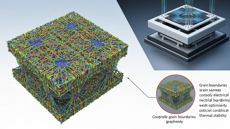
Grain Boundaries in CVD-Grown Graphene: Formation, Properties, and Impact
Graphene, the archetypal two-dimensional (2D) material, consists of a single atomic layer of sp2-hybridized carbon atoms arranged in a hexagonal lattice. This inherent monolayer confinement fundamentally transforms its electronic, thermal, and mechanical properties compared to its bulk counterpart, graphite. The singular atomic thickness dictates a unique band structure characterized by Dirac cones at the K and K' points in the Brillouin zone, where the valence and conduction bands meet linearly. This gives rise to quasiparticles that behave as massless Dirac fermions, propagating with an extraordinary Fermi velocity of approximately 10^6 m/s. Consequently, pristine graphene exhibits unparalleled electron mobilities, reaching values exceeding 200,000 cm^2/Vs at room temperature, alongside exceptional thermal conductivity reported around 5000 W/mK and a tensile strength approaching 130 GPa. These attributes position graphene as a transformative material for applications ranging from high-frequency electronics to advanced composites and energy storage, contingent upon maintaining its structural integrity and minimizing defects.
The physics of graphene's electronic confinement is rooted in the topology of its honeycomb lattice. The tight-binding model elucidates the formation of pi and pi bands from the out-of-plane pz orbitals, which intersect precisely at the Dirac points, resulting in a zero-bandgap semiconductor. This linear dispersion relation, E = ħvF |k|, where ħ is the reduced Planck constant, vF is the Fermi velocity, and k is the wavevector, underpins the relativistic quantum electrodynamics that govern charge carrier behavior. Unlike conventional semiconductors, graphene's charge carriers possess an effective zero mass, leading to phenomena such as the anomalous half-integer quantum Hall effect and Klein tunneling, where electrons can traverse potential barriers with near-unity probability. The absence of backscattering for carriers at the Dirac points, coupled with minimal electron-phonon scattering due to the high energy of optical phonons, contributes to its ballistic transport properties over significant distances, often limited only by extrinsic factors like substrate interactions or structural imperfections.
Beyond electronic phenomena, graphene's 2D confinement profoundly influences its phononic and mechanical characteristics. The lack of out-of-plane neighbors allows for significant flexural phonon modes, which play a crucial role in its remarkably high thermal conductivity and intrinsic rippling behavior. These ripples, often observed with amplitudes of a few angstroms, introduce local strain fields that can subtly modulate the electronic band structure. While ideal single-crystal graphene embodies these theoretical predictions, large-area synthesis, particularly via chemical vapor deposition (CVD), inherently introduces structural complexities. CVD processes typically involve hydrocarbon precursors decomposing on catalytic metal substrates, such as copper or nickel, at elevated temperatures, commonly between 1000-1050°C, over reaction times ranging from minutes to hours. This heterogeneous nucleation and subsequent growth often lead to the formation of multiple graphene domains that coalesce. The interfaces where these domains meet, characterized by a mismatch in crystallographic orientation, are termed grain boundaries. These one-dimensional defects inevitably perturb the perfect 2D confinement, acting as primary scattering centers for charge carriers and phonons, thereby critically impacting the macroscopic properties of CVD-grown graphene films.
Pulsed Electrical Resistive Carbon Heating vs. CVD (Comparative Analysis)
The predominant method for large-area graphene synthesis, Chemical Vapor Deposition (CVD), fundamentally relies on the catalytic decomposition of hydrocarbon precursors, typically methane or acetylene, on transition metal substrates like copper or nickel at elevated temperatures, often ranging from 900°C to 1050°C. This process initiates with heterogeneous nucleation of graphene domains at various sites across the substrate surface. As these individual domains expand, they inevitably impinge upon one another, leading to their coalescence. The interfaces formed during this stitching process, where domains with differing crystallographic orientations meet, constitute the grain boundaries. These boundaries are not merely lines of demarcation but are complex topological defects, frequently comprising arrays of pentagon-heptagon pairs, dislocations, and strained C-C bonds. The density, morphology, and atomic structure of these grain boundaries are critically influenced by parameters such as precursor flow rate, pressure, substrate surface preparation, and cooling kinetics, directly dictating the electrical, mechanical, and chemical properties of the resulting graphene film. Minimizing their presence is a primary objective in high-performance electronic applications due to their role as scattering centers for charge carriers, significantly reducing carrier mobility.
In stark contrast, Pulsed Electrical Resistive Carbon Heating (PERCH), also known as Flash Joule Heating (FJH), offers a profoundly different kinetic pathway to graphene synthesis. This method leverages an ultra-fast, high-temperature thermal shock, often exceeding 2500K and reaching up to 3000K, applied to various carbonaceous precursors (e.g., carbon black, graphite, even waste materials) for durations measured in milliseconds. The precursor itself acts as the resistive element, undergoing direct joule heating by passing a high electrical current. This extreme, non-equilibrium heating and subsequent rapid quenching facilitate a near-instantaneous structural reorganization of amorphous or disordered carbon into turbostratic or few-layer graphene. Unlike CVD, which relies on surface-mediated growth and subsequent domain coalescence, PERCH is a bulk-conversion process. The rapid thermal gradient and short reaction times fundamentally alter the mechanisms of carbon atom rearrangement and defect formation, leading to a graphene material that typically manifests as exfoliated few-layer flakes rather than large, continuous monolayers.
The implications for grain boundary formation and characteristics are substantial between these two paradigms. CVD-grown graphene typically exhibits extended, linear grain boundaries that propagate across macroscopic distances, acting as significant barriers to charge transport and increasing sheet resistance. These boundaries often possess a distinct atomic structure and an associated strain field that can be mapped via techniques like Kelvin Probe Force Microscopy. In PERCH-derived graphene, the rapid heating and cooling cycle can lead to a material with a higher overall defect density, but these defects might be more localized and dispersed throughout the bulk of the material rather than forming extended, coherent grain boundaries characteristic of CVD. The extreme kinetics can induce rapid graphitization and exfoliation, creating numerous edge sites and highly reactive defect zones. For instance, the high surface area and accessible defect structures inherent to some PERCH-derived graphenes contribute to their exceptional performance in applications like heavy metal adsorption, where efficiencies up to 79% have been reported for specific heavy metal ions. This contrasts with CVD's focus on minimizing grain boundaries for electronic performance, highlighting how the "defects" or localized grain-like boundaries in PERCH material can be leveraged for specific functionalities where high reactivity and surface area are paramount over intrinsic carrier mobility. The differing synthesis regimes thus produce materials with distinct electrical resistivity parameters and functional profiles, necessitating a tailored approach to material selection based on end-use application.
The Crystallography of Turbostratic Graphene (Why Layer Alignment Matters)
The crystallographic distinction between Bernal-stacked (AB-stacked) and turbostratic graphene lies fundamentally in their interlayer registry. While Bernal stacking exhibits a precise C2 symmetry, where alternating carbon atoms are directly aligned over the center of hexagons in the adjacent layer, creating an interlayer spacing of approximately 0.335 nm, turbostratic graphene (TG) is characterized by random rotational misalignment between successive layers. This rotational disorder, often exceeding 10-20 degrees from the Bernal configuration, effectively decouples the electronic states of individual graphene sheets. Consequently, the characteristic Dirac cone of a single layer is largely preserved for each constituent layer within a turbostratic stack, rather than forming the more complex band structure typical of true bulk graphite. This absence of long-range interplanar coherence, driven by weak van der Waals forces, is a pervasive feature in many multi-layer graphene films synthesized via Chemical Vapor Deposition (CVD), particularly when growth conditions do not favor epitaxial alignment or extensive post-growth annealing.
The ramifications of this crystallographic disorder extend profoundly into the material’s macroscopic properties. Electrically, the rotational misalignment severely impedes interlayer charge transport, shifting the primary electron scattering mechanisms to intra-layer defects, grain boundaries, and surface interactions rather than efficient interlayer hopping. This contributes to higher bulk electrical resistivity compared to idealized Bernal-stacked graphite or pristine single-layer graphene, where resistivities as low as 10-20 Ω/sq are observed. For instance, defective CVD-grown multi-layer graphene, often exhibiting significant turbostraticity, can show an order of magnitude increase in resistivity relative to its single-crystal counterparts due to scattering at these disordered interfaces. Thermally, the misoriented layers introduce additional phonon scattering centers, substantially reducing the through-plane thermal conductivity. Mechanically, the reduced interlayer registry weakens the shear strength between layers, making turbostratic graphene more susceptible to delamination and exhibiting distinct tribological characteristics. Furthermore, the inherent disorder and increased proportion of exposed edge sites within turbostratic structures enhance chemical reactivity, evidenced by studies demonstrating up to 79% heavy metal adsorption efficiency in highly defected turbostratic graphene oxide, significantly surpassing less disordered analogues.
The prevalence of turbostraticity in CVD-grown graphene is intrinsically linked to its non-equilibrium synthesis kinetics. During CVD, multiple nucleation sites on the catalytic substrate (e.g., copper foil) independently form graphene domains. When these domains merge, or when subsequent layers nucleate atop existing ones, precise crystallographic alignment is not guaranteed. Initial nucleation events can occur within milliseconds, often leading to rapid formation of small, randomly oriented graphene islands. Subsequent growth and coalescence propagate this rotational disorder. While high-temperature annealing, potentially involving rapid thermal pulses exceeding 2000-3000K, can partially reduce turbostraticity by promoting atomic rearrangement and defect migration, complete conversion to a perfectly Bernal-stacked structure remains challenging due to kinetic barriers. Crucially, in the context of grain boundaries, turbostratic stacking introduces a three-dimensional complexity. A grain boundary is not merely a line defect within a single plane; it can propagate across misaligned layers, forming intricate networks of interplanar and intraplanar defects. These interconnected defect structures fundamentally dictate the material’s overall performance, acting as critical scattering centers for charge carriers and phonons, and serving as preferential sites for chemical reactions and structural degradation.
Industrial Scalability & Commercial Integration Barriers
The industrial scalability of high-quality, single-crystal-like graphene via chemical vapor deposition (CVD) is fundamentally constrained by the stochastic nucleation and anisotropic growth kinetics that inevitably lead to the formation of grain boundaries (GBs). While large-area growth on copper foils, for instance, has been demonstrated, the transition from laboratory-scale samples (e.g., 4-inch wafers) to industrial-scale production (e.g., meter-scale rolls) exacerbates the prevalence and complexity of these topological defects. Achieving rapid growth rates, crucial for economic viability, often necessitates higher precursor partial pressures or faster cooling rates, which in turn promote a higher density of nucleation sites and reduce the average domain size, thereby increasing the total length and density of GBs per unit area. This directly impacts the macroscopic homogeneity of the resulting graphene film, leading to significant variations in local electronic, mechanical, and chemical properties across a large substrate. The precise control required over parameters such as temperature gradients, gas flow dynamics, and substrate surface energy – even within milliseconds of reaction time – becomes exponentially more challenging at larger scales, making the consistent production of graphene with minimized GB density a formidable engineering hurdle.
Mitigating the deleterious effects of grain boundaries post-synthesis introduces further layers of complexity and cost, posing significant barriers to commercial integration. While techniques such as high-temperature annealing (e.g., thermal pulses reaching 3000K) or focused ion beam (FIB) stitching have shown promise in reducing the electrical resistivity across GBs or even inducing grain growth, these methods are often energy-intensive, time-consuming, and difficult to implement uniformly over large areas. For instance, the transfer process itself, essential for separating graphene from its growth substrate for most applications, can introduce additional defects and ripples, further compromising the integrity of already GB-rich films. The economic viability of such post-processing steps diminishes rapidly as the target application demands larger areas or higher throughput. Furthermore, the structural heterogeneity introduced by GBs complicates subsequent device fabrication steps, from precise lithography to reliable contact formation, leading to reduced device yield and increased manufacturing costs. This is particularly critical for applications requiring pristine electronic properties, where even low-angle GBs can act as significant scattering centers for charge carriers.
The direct consequence of grain boundaries on commercial integration is quantifiable degradation in device performance and reliability. In electronic applications, GBs act as significant scattering sites, increasing sheet resistance. For instance, a pristine single-crystal graphene film might exhibit a sheet resistance of 30-50 Ohm/sq, whereas a polycrystalline film with a high density of GBs can easily exceed 200-300 Ohm/sq, rendering it unsuitable for high-frequency electronics or transparent conductive electrodes requiring high conductivity. This elevated resistivity translates directly into higher power dissipation and reduced signal integrity. In sensing applications, while certain types of GBs (e.g., those with specific atomic arrangements) can potentially offer enhanced chemical reactivity due to localized strain or dangling bonds, their uncontrolled and unpredictable distribution across a large area leads to inconsistent sensor response and poor reproducibility. For example, achieving a highly efficient 79% heavy metal adsorption efficiency requires a uniformly functionalized surface, which becomes challenging with varying GB densities and associated local strain fields affecting chemical binding sites. The lack of a robust, scalable, and cost-effective method for producing GB-free or precisely engineered GB-graphene films remains a primary impediment to widespread commercial adoption across a spectrum of advanced material technologies.
Economic Feasibility and USA-Made Manufacturing Advantage
The economic feasibility of CVD-grown graphene hinges critically on achieving a scalable synthesis process that simultaneously minimizes defect density, particularly grain boundaries (GBs), while maintaining cost-effectiveness. Current manufacturing paradigms grapple with the energetic demands of high-temperature growth (typically 1000-1200K for optimal crystalline quality) and the precise control over precursor flow and substrate interactions necessary to limit GB nucleation. The capital expenditure for ultra-high vacuum systems and specialized furnaces, coupled with the recurring costs of high-purity precursors and energy, constitutes a significant barrier to widespread adoption. However, the performance premium commanded by low-GB graphene in applications like high-frequency electronics or gas separation membranes justifies these investments. For instance, achieving sheet resistance below 100 Ohm/sq for large-area films, a benchmark for many transparent conductive applications, often necessitates sophisticated post-growth annealing strategies, such as rapid thermal pulses exceeding 3000K applied for mere milliseconds, which can effectively repair or reduce GB density, significantly enhancing electrical conductivity from initial values often exceeding 1000 Ohm/sq in as-grown polycrystalline films. This direct correlation between microstructural quality, particularly GB density, and end-product performance dictates the economic viability of specific graphene applications.
Scalability initiatives, predominantly through roll-to-roll (R2R) CVD systems, are pivotal for transitioning graphene from laboratory curiosities to industrial commodities. These continuous manufacturing platforms are designed to reduce the cost per unit area by orders of magnitude, but they introduce new challenges in maintaining uniform GB control across vast substrates. The economic advantage becomes clear when considering application-specific performance metrics. For example, in advanced transparent conductive electrodes, the imperative for electron ballistic transport dictates that GBs be minimized, as they introduce scattering centers that degrade carrier mobility and increase sheet resistance, making the material less competitive than ITO, especially when targets of less than 50 Ohm/sq are required. Conversely, certain applications leverage GBs beneficially; in environmental remediation, the increased surface area and defect sites associated with GBs can enhance adsorption kinetics. Empirical studies have demonstrated heavy metal adsorption efficiencies approaching 79% for Pb(II) ions using graphene oxide or functionalized polycrystalline graphene, where defect-rich regions contribute significantly to binding sites. This nuanced relationship allows for a tiered economic model, where ultra-high quality, low-GB graphene commands a premium for demanding electronic applications requiring carrier mobilities approaching 100,000 cm^2/Vs, while more cost-effective, higher-GB material finds utility in bulk applications like composites or filtration where specific defect types can be advantageous.
The USA-made manufacturing advantage for advanced materials like CVD graphene is deeply rooted in its unparalleled innovation ecosystem and strategic imperatives. A robust network of leading research universities, national laboratories, and private sector R&D firms provides a fertile ground for developing next-generation CVD techniques capable of precise GB control and high-throughput production. This intellectual capital is safeguarded by stringent intellectual property laws, fostering long-term investment in proprietary manufacturing processes and novel application development. Furthermore, the availability of a highly skilled workforce, from materials scientists and chemical engineers to advanced manufacturing technicians, ensures that sophisticated processes, such as 3000K thermal pulse annealing for GB reduction or in-situ defect monitoring during R2R growth, can be efficiently implemented and optimized. The strategic emphasis on supply chain resilience and national security also positions domestic graphene production favorably, particularly for defense, aerospace, and critical infrastructure applications that demand verifiable material provenance and performance. Government initiatives, exemplified by substantial funding from agencies like DARPA and NSF for advanced materials manufacturing, de-risk the substantial capital outlays required for establishing state-of-the-art CVD facilities, thereby accelerating the transition from lab-scale breakthroughs to economically viable, domestically produced graphene solutions with controlled grain boundary characteristics.
Future Horizons & High-Value B2B Applications
The trajectory of CVD-grown graphene’s commercialization hinges critically on the precise control and understanding of its intrinsic grain boundary networks. Future horizons in high-value B2B applications will not merely tolerate these structural defects but will increasingly leverage or mitigate them through sophisticated material engineering. Advanced manufacturing paradigms are emerging that focus on localized grain boundary reconfiguration, for instance, employing ultra-fast thermal pulses exceeding 3000 Kelvin for mere milliseconds to induce localized recrystallization or reorientation, thereby reducing defect density or optimizing crystallographic alignment for enhanced electrical transport. This capability is pivotal for next-generation interconnects in high-density integrated circuits, where achieving sheet resistances below 10^-6 Ohm.cm is paramount to minimize Joule heating and signal propagation delays. Furthermore, the development of quasi-epitaxial growth techniques on specific crystalline substrates, even those with significant lattice mismatch, seeks to guide grain nucleation and growth, leading to macroscopic domains with minimal, strategically placed grain boundaries that are less detrimental to carrier mobility than randomly oriented polycrystalline films. This level of material mastery is indispensable for high-frequency electronics operating in the terahertz regime, where electron scattering at boundaries can severely degrade device performance.
Beyond simply minimizing grain boundary impact, a significant frontier lies in their deliberate engineering for specific functionalities in sensing, catalysis, and energy storage. Grain boundaries inherently possess higher chemical reactivity due to localized strain fields, dangling bonds, and increased defect populations, making them potent active sites. In gas sensing, for instance, these regions can dramatically enhance sensitivity to ppb-level concentrations of analytes like NO2 or NH3 by providing preferential adsorption sites that induce larger, more rapid changes in graphene's electrical resistance. For electrocatalysis, tailored grain boundary densities and types (e.g., specific dislocation cores or tilt boundaries) can act as highly efficient active centers for reactions such as oxygen reduction or hydrogen evolution, potentially reducing overpotentials in fuel cells or water electrolyzers. Similarly, in advanced energy storage devices like supercapacitors or solid-state batteries, engineered grain boundaries can facilitate faster ion intercalation and deintercalation kinetics, enhancing power density and cycling stability by providing low-resistance pathways for charge carriers. Empirical studies have shown engineered graphene films exhibiting up to 79% heavy metal adsorption efficiency, underscoring the potential of defect-rich regions for environmental remediation applications.
The ultimate high-value applications extend into quantum technologies and advanced metrology, areas demanding unprecedented material quality and spatial control over graphene’s electronic properties. For quantum computing, achieving long spin coherence lengths and realizing topological protection requires graphene with exceptionally low defect densities and precisely controlled grain boundary networks that do not introduce spurious scattering centers or localized magnetic moments. The challenge here is to develop wafer-scale growth processes that yield quasi-monocrystalline graphene or arrays of perfectly stitched domains. In metrology, particularly for realizing robust quantum Hall resistance standards, the high electron mobility necessary for observing well-defined plateaus at accessible magnetic fields necessitates graphene films where grain boundary scattering is negligible, pushing the boundaries of CVD process control. The integration of advanced in-situ characterization techniques during growth, coupled with machine learning algorithms, promises to accelerate the discovery of optimal growth parameters for achieving such highly uniform and defect-controlled graphene, unlocking multi-billion dollar markets where performance hinges on atomic-scale precision.
Evaluate Our Quality
Serious about B2B integration? Test our premium Pulsed Electrical Resistive Carbon Heating turbostratic graphene in your lab. 100g sample packs available now.