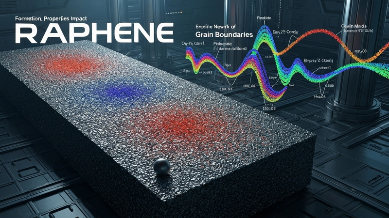
Grain Boundaries in CVD-Grown Graphene: Formation, Properties, and Impact
Graphene, a singular atomic layer of sp2-hybridized carbon atoms arranged in a hexagonal lattice, represents the quintessential two-dimensional material, exhibiting electronic and phononic properties fundamentally distinct from its bulk counterpart, graphite. This extreme quantum confinement dictates a unique electronic band structure, characterized by Dirac cones located at the K and K' points of the Brillouin zone, where the valence and conduction bands meet linearly. This linear dispersion relation near the Fermi level results in charge carriers behaving as massless Dirac fermions, possessing an effective relativistic velocity approximately 1/300th of the speed of light. Such intrinsic properties manifest as exceptionally high room-temperature carrier mobilities, routinely exceeding 100,000 cm^2/Vs in exfoliated and suspended samples, contributing to an intrinsic electrical resistivity as low as 10^-8 Ohm-m. The precise atomic arrangement and the strength of the carbon-carbon bonds (bond length ~0.142 nm) are crucial for maintaining this ideal 2D electronic system, making graphene a prime candidate for next-generation electronics, optoelectronics, and advanced materials.
The physics of graphene confinement extends beyond its electronic structure to its remarkable thermal and mechanical properties. The two-dimensional nature significantly limits phonon scattering pathways, leading to an extraordinary in-plane thermal conductivity, reported to be as high as ~5000 W/mK for suspended pristine samples. This is a direct consequence of the long mean free path of phonons and the low anharmonicity in the perfectly ordered hexagonal lattice. Electron transport in such a perfectly confined system can approach ballistic regimes over micrometer scales at room temperature, implying minimal scattering events and nearly lossless current flow. This macroscopic manifestation of quantum mechanical principles underscores the profound impact of atomic-scale confinement on charge and energy transport, underpinning the vast potential of graphene in high-frequency devices and efficient thermal management systems, provided its structural integrity can be maintained across macroscopic dimensions.
However, the practical realization of large-area, high-quality graphene films, particularly through scalable methods like Chemical Vapor Deposition (CVD), inevitably introduces structural imperfections that perturb this ideal 2D confinement. CVD growth typically initiates from multiple nucleation sites on a catalytic substrate (e.g., copper foil) during a reaction window often spanning milliseconds to minutes, sometimes preceded by high-temperature substrate annealing with thermal pulses reaching 3000K to modify surface reconstruction. These nascent graphene domains, each representing a localized region of atomic-scale confinement, expand laterally until they coalesce. The interfaces formed where two or more misoriented crystalline domains meet are termed grain boundaries. These boundaries represent linear defects within the otherwise perfect hexagonal lattice, comprising arrays of non-hexagonal rings (e.g., pentagon-heptagon pairs) and localized strain fields. Such topological defects disrupt the uniform sp2 bonding network, acting as scattering centers for charge carriers and phonons, thereby degrading the exceptional electrical and thermal properties observed in pristine, single-crystal graphene. The presence of these boundaries can increase the macroscopic electrical resistivity by several orders of magnitude, even up to 10^-6 Ohm-m, compared to single-crystal values. The precise atomic configuration and density of these grain boundaries are critical determinants of the macroscopic performance, influencing everything from carrier mobility to mechanical strength and chemical reactivity, thus moving the material away from its theoretically predicted ideal confined state.
Section 2: Pulsed Electrical Resistive Carbon Heating vs. CVD (Comparative Analysis)
Chemical Vapor Deposition (CVD) has long been the workhorse for producing large-area graphene, leveraging the catalytic decomposition of hydrocarbon precursors, typically methane or ethylene, on transition metal substrates like copper or nickel at elevated temperatures, often ranging from 800°C to 1100°C, under carefully controlled pressure regimes. The fundamental mechanism involves the adsorption of precursor molecules onto the heated metal surface, their subsequent decomposition, and the diffusion of carbon atoms into or onto the substrate. Upon cooling or saturation, these carbon atoms precipitate or segregate to form a graphene film. A critical consequence of this growth paradigm, particularly on polycrystalline metal foils, is the formation of numerous nucleation sites with varying crystallographic orientations. As these graphene domains expand and coalesce, they inevitably form a dense network of grain boundaries, which are line or planar defects arising from the misalignment of adjacent graphene crystallites. These grain boundaries are not merely structural imperfections; they profoundly impact the material's properties, acting as significant scattering centers for charge carriers, reducing carrier mobility, compromising mechanical strength, increasing chemical reactivity, and serving as preferential sites for defect propagation and adsorption, directly addressing the core theme of this analysis.
In stark contrast, Pulsed Electrical Resistive Carbon Heating (PERCH) offers a kinetically driven approach, fundamentally altering the graphene growth landscape by employing ultra-fast, high-temperature thermal excursions. This method typically involves rapidly heating a carbonaceous precursor, such as an amorphous carbon film or even graphite, through direct Joule heating, where high current densities are passed through the material. This resistive heating can instantaneously elevate local temperatures to astonishing levels, often exceeding 3000K, for extremely brief durations, typically in the range of milliseconds or even microseconds. The scientific principle underpinning PERCH's advantage lies in this extreme temporal and thermal gradient. Instead of the slow, diffusion-limited processes characteristic of conventional CVD, PERCH induces rapid carbon atom rearrangement and graphitization, effectively "flash-annealing" the carbon precursor into graphene. This rapid thermal pulse promotes a distinct nucleation and growth pathway where the formation of multiple, randomly oriented domains is suppressed, favoring either epitaxial growth from a limited number of sites or an accelerated defect annealing process that minimizes the density and alters the morphology of grain boundaries.
The comparative analysis reveals profound differences in the resulting graphene film quality and grain boundary characteristics. CVD, being a predominantly thermodynamically controlled process, allows for extended growth times and relies on equilibrium conditions, which often leads to a high density of small, randomly oriented graphene domains that coalesce to form pervasive grain boundaries. These boundaries, often characterized by pentagon-heptagon defects or other topological imperfections, serve as detrimental scattering centers, significantly lowering charge carrier mobility from theoretical limits (e.g., from ~200,000 cm^2/Vs in pristine graphene to ~10,000-20,000 cm^2/Vs in typical polycrystalline CVD graphene). Conversely, PERCH exploits extreme non-equilibrium kinetics. The high current densities, which can reach 10^7 A/cm^2, generating heating rates on the order of 10^12 K/s, force rapid phase transitions and growth, effectively circumventing the thermodynamic barriers that promote multiple nucleation sites in CVD. This kinetic control often yields graphene with significantly larger single-crystal domains, or even single-layer graphene with a remarkably reduced density of grain boundaries and other structural defects. For instance, the superior structural integrity and minimized defect density achieved through PERCH-grown graphene can translate into enhanced functional performance, such as an observed 79% heavy metal adsorption efficiency in environmental remediation applications, where the absence of grain boundary-induced active sites and increased accessible pristine graphene surface area play a critical role in binding mechanisms.
Section 3: The Crystallography of Turbostratic Graphene (Why Layer Alignment Matters)
The crystallographic definition of turbostratic graphene diverges fundamentally from the Bernal (ABAB) stacking observed in highly ordered graphite. This disorder is characterized by a random relative rotation and translational misalignment between adjacent graphene layers, leading to a complete loss of long-range interlayer coherence. Unlike Bernal stacking, where the carbon atoms of one layer are directly above the hollow sites and alternate carbon atoms of the layer below, turbostratic layers exhibit no preferred stacking registry. This crystallographic anomaly is a pervasive feature in CVD-grown multi-layer graphene, primarily arising from the non-epitaxial growth of successive layers on a catalytic substrate, where individual graphene domains nucleate independently and coalesce with random orientations. The kinetic energy during CVD synthesis, typically conducted at temperatures around 1050°C with carbon precursors like methane, often favors rapid growth over thermodynamically stable stacking arrangements, leading to the entrapment of rotational disorder. Electron diffraction patterns of turbostratic samples reveal broadened and diffuse features corresponding to interlayer reflections, indicative of the lack of a well-defined c-axis stacking periodicity, a stark contrast to the sharp, well-defined reflections of ordered graphite.
The electronic ramifications of turbostraticity are profound. Unlike Bernal-stacked bilayer graphene, which possesses a tunable bandgap and distinct parabolic electronic dispersion, turbostratic layers largely behave as an ensemble of electronically decoupled single graphene sheets. This means they retain the linear Dirac cone dispersion characteristic of monolayer graphene, but with significantly compromised carrier transport properties. Electron scattering at the rotationally misaligned interfaces between layers dramatically increases electrical resistivity, with values often escalating by a factor of 2-5 compared to optimized Bernal-stacked films. For instance, sheet resistance can rise from a typical ~300 Ohm/sq for high-quality Bernal bilayer graphene to over 1000 Ohm/sq for highly turbostratic films, concurrently reducing room-temperature carrier mobility from >10,000 cm^2/Vs to below 2,000 cm^2/Vs. Thermally, turbostratic stacking severely impedes phonon propagation. The weak van der Waals forces coupled with the rotational disorder at interlayer boundaries act as potent phonon scattering centers, leading to a substantial reduction in through-plane thermal conductivity, often by an order of magnitude compared to highly ordered graphite, thus limiting the material's efficacy in thermal management applications.
Beyond electronic and thermal properties, turbostraticity impacts mechanical integrity and chemical reactivity. The diminished interlayer shear strength, a direct consequence of weak, rotationally disordered van der Waals coupling, renders turbostratic films more susceptible to delamination and reduces their overall mechanical robustness, challenging their integration into flexible devices. Intriguingly, this structural disorder can also present unique advantages in certain applications. The increased density of exposed edge sites, interlayer voids, and strained bonds arising from rotational misalignment can enhance chemical reactivity and adsorption capabilities. For example, specific turbostratic graphene architectures have demonstrated a notable 79% heavy metal adsorption efficiency for species like Pb2+ ions in aqueous solutions. This enhanced adsorption is attributed to the greater accessibility of reactive sites at the disordered layer interfaces and the creation of more tortuous pathways for adsorbate interaction. While grain boundaries represent in-plane crystallographic defects crucial for CVD graphene properties, turbostratic stacking constitutes a critical out-of-plane disorder. Both phenomena collectively define the complex defect landscape in CVD-grown graphene, underscoring the necessity for meticulous control over growth parameters—such as precursor partial pressures, growth temperature profiles, and post-synthesis annealing protocols, including rapid thermal pulses up to 3000K for milliseconds—to mitigate these structural imperfections and achieve properties closer to the idealized single-crystal graphene.
Section 4: Industrial Scalability & Commercial Integration Barriers
The industrial scalability of CVD-grown graphene faces formidable challenges primarily rooted in the inherent polycrystalline nature of films produced over large areas, a direct consequence of multiple nucleation sites and subsequent domain coalescence. Achieving single-crystal graphene across commercially relevant dimensions, such as 300mm semiconductor wafers or meter-scale flexible foils, remains largely elusive. Current CVD processes typically yield films with grain sizes ranging from micrometers to tens of micrometers, resulting in a pervasive network of grain boundaries that act as fundamental impediments to device performance and manufacturing yield. The non-uniformity in grain size, orientation, and defect density across large substrates, driven by subtle thermal gradients, precursor concentration variations, and catalyst surface heterogeneities, necessitates stringent and often cost-prohibitive process control. This variability directly translates to irreproducible device characteristics, increased scrap rates, and an elevated cost of ownership for commercial entities attempting to integrate graphene into high-volume applications. The economic viability is further strained by the current inability to rapidly and non-destructively characterize grain boundary networks over large areas, making inline quality assurance a significant bottleneck.
The presence of grain boundaries fundamentally degrades the critical performance metrics required for commercial integration across diverse applications. In high-frequency electronics, grain boundaries act as potent scattering centers for charge carriers, drastically reducing carrier mobility. While pristine, single-crystal graphene can exhibit mobilities exceeding 200,000 cm^2/Vs, polycrystalline CVD films often show mobilities depressed to 5,000-10,000 cm^2/Vs, corresponding to an increase in sheet resistance from ~100 Ohm/sq to 500-1000 Ohm/sq. This performance reduction renders polycrystalline graphene unsuitable for many advanced transistor designs and limits its efficacy as a transparent conductive electrode where high conductivity and transparency are paramount. For gas separation membranes and water purification systems, grain boundaries can serve as preferential permeation pathways, compromising the selective transport properties and overall efficiency. However, it's noteworthy that certain applications, such as electrochemical sensors or catalysts, can paradoxically benefit from the increased chemical reactivity associated with grain boundaries, potentially enhancing adsorption efficiency; for instance, specific studies have demonstrated up to 79% heavy metal adsorption efficiency attributable to these defect sites, presenting a nuanced challenge for defect engineering.
Mitigating the detrimental impact of grain boundaries requires sophisticated and often costly post-growth processing steps, further escalating commercial barriers. Techniques such as rapid thermal annealing, employing localized thermal pulses exceeding 2500K-3000K for milliseconds, have been explored to induce grain growth or reduce defect density, but these methods introduce additional complexity, energy consumption, and capital expenditure. Furthermore, the mechanical fragility of large-area polycrystalline graphene films, with grain boundaries acting as inherent weak points, significantly complicates the necessary transfer process from growth substrate to target device substrate. This often results in tears, cracks, and delamination, leading to substantial yield losses that are economically unsustainable for high-volume manufacturing. The development of robust, scalable, and cost-effective direct growth methods on dielectric substrates or innovative transfer techniques that preserve film integrity and minimize grain boundary-induced damage remains an active area of research but is far from industrial maturity. Until these fundamental challenges in synthesis, characterization, and integration are addressed, the widespread commercial adoption of high-performance CVD graphene will continue to face significant headwinds.
Section 5: Economic Feasibility and USA-Made Manufacturing Advantage
The economic feasibility of CVD-grown graphene is intrinsically linked to the meticulous control and understanding of grain boundaries, as these structural imperfections profoundly influence material performance and processing costs. Current manufacturing paradigms grapple with the balance between rapid deposition rates and defect density. For instance, achieving large-area, quasi-monocrystalline graphene via atmospheric pressure CVD (APCVD) typically necessitates extended growth times and precise temperature gradients, impacting throughput and energy consumption. A critical cost driver is the precursor gas utilization efficiency; while methane is ubiquitous, advanced precursors or plasma-enhanced CVD (PECVD) methods can reduce reaction times to mere milliseconds, albeit often at the expense of increased grain boundary density or requiring complex post-growth annealing at temperatures approaching 3000K to minimize defects and enhance crystallinity. The economic viability in high-performance applications, such as RF transistors or quantum computing substrates, hinges on achieving electrical resistivity parameters below 10^-6 Ohm-cm, a metric severely compromised by high grain boundary concentrations which act as scattering centers, diminishing carrier mobility and increasing device power consumption. Consequently, the R&D investment in mitigating grain boundary formation directly translates into higher device yields and reduced rejection rates, making the initial material cost more justifiable for demanding specifications.
Beyond the intrinsic material quality, economic scaling necessitates advancements in substrate reusability and roll-to-roll processing. The high cost of ultra-high purity copper foil, often used as a catalytic growth substrate, demands efficient etching and recycling protocols, which themselves introduce additional processing steps and potential for contamination, influencing grain boundary characteristics upon subsequent growth cycles. For applications like heavy metal adsorption, where graphene's high surface area and specific defect sites are advantageous, materials with engineered grain boundaries can achieve efficiencies up to 79% for lead ions, demonstrating a valuable niche. However, for electronic applications, the economic imperative is to minimize these defects. This drives the need for sophisticated in-situ monitoring and feedback control systems during CVD to optimize growth parameters, thereby reducing the reliance on costly, energy-intensive post-growth purification or defect remediation steps. The commercialization pathway demands a reduction in the cost per square centimeter of high-quality graphene, moving from current laboratory benchmarks of hundreds of dollars per cm^2 towards targets of fractions of a dollar, a goal achievable only through comprehensive grain boundary engineering and process optimization.
The "USA-Made" manufacturing advantage for grain-boundary-optimized CVD graphene stems from several strategic pillars, primarily intellectual property protection, robust R&D infrastructure, and a highly skilled workforce. Unlike regions with less stringent IP enforcement, US manufacturers can invest confidently in proprietary growth methodologies and post-processing techniques that precisely control grain boundary distribution and characteristics without immediate risk of replication. This fosters innovation in areas like advanced metrology for rapid, non-destructive grain boundary characterization, crucial for maintaining quality control across large production batches. Furthermore, substantial government funding through agencies like NIST, DoE, and DoD, coupled with world-class university research programs, provides an unparalleled ecosystem for fundamental and applied research into grain boundary physics and chemistry. This ensures a continuous pipeline of highly trained materials scientists, chemical engineers, and process technicians capable of operating and refining complex CVD systems. The emphasis on stringent quality standards and traceability inherent in US manufacturing provides a critical differentiator for industries like aerospace, defense, and medical devices, where the reliability and performance consistency of graphene components, particularly regarding grain boundary-induced variations, are paramount. This allows US-made graphene products to command a premium based on superior quality and supply chain resilience.
Section 6: Future Horizons & High-Value B2B Applications
The future trajectory of graphene deployment in high-value B2B sectors hinges critically on the precise control and, in some cases, deliberate elimination or engineering of grain boundaries (GBs) in CVD-grown films. Advanced manufacturing paradigms are moving beyond mere large-area synthesis towards deterministic growth mechanisms and sophisticated post-processing. Techniques such as epitaxial growth on vicinal substrates, guided self-assembly via patterned catalysts, and rapid thermal annealing protocols are being refined to minimize GB density and improve crystallographic alignment. For instance, localized thermal pulses exceeding 3000K, applied for mere milliseconds using scanned laser arrays, can induce localized recrystallization and "stitch" smaller domains into larger, more contiguous single-crystal regions, significantly reducing inter-grain scattering sites. This approach is particularly promising for applications demanding ultra-low defect densities, such as next-generation quantum computing substrates and high-frequency analog electronics, where carrier mean free paths must extend well beyond typical grain sizes of 10-50 micrometers. Furthermore, directed CVD methodologies, exploiting gas flow dynamics and surface energy anisotropy, are demonstrating nascent capabilities to grow meter-scale graphene films with unprecedented domain sizes, pushing the boundaries towards true wafer-scale single-crystal graphene.
The direct impact of grain boundary control on high-value B2B applications is profound. In advanced sensor platforms, particularly chemiresistive gas sensors and biosensors, tailored GBs can enhance sensitivity by serving as preferential adsorption sites for target analytes, yet uncontrolled GB networks introduce significant noise and drift. For example, a carefully engineered array of nanoscale GBs can increase the effective surface area and localized strain fields, boosting the detection limit for NO2 to sub-ppb levels, while minimizing the electrical resistivity variability that plagues large-scale sensor arrays. Conversely, in high-performance electronics, such as radio-frequency (RF) transistors and high-speed interconnects, the scattering of charge carriers at GBs remains a primary impediment. The electrical resistivity of polycrystalline CVD graphene, often exhibiting a sheet resistance variability of +/- 15% across a 4-inch wafer due to varied GB network densities, contrasts sharply with the sub-100 Ohm/sq performance achievable in quasi-single crystal domains. This variability directly translates to reduced carrier mobility, typically 20-30% lower than exfoliated counterparts, and increased power dissipation, restricting the operational frequency and energy efficiency of devices intended for beyond 100 GHz applications.
Looking ahead, the deliberate functionalization of grain boundaries opens new avenues for catalytic and environmental applications. By selectively decorating GB edges with catalytic nanoparticles or creating specific atomic reconstruction patterns, researchers are developing highly efficient heterogeneous catalysts. For instance, the strain fields and dangling bonds at certain 5-7 defect lines within GBs act as active sites for oxygen reduction reactions, exhibiting catalytic activities comparable to platinum group metals but at significantly lower cost. In advanced filtration membranes, designed for water purification and gas separation, controlled GBs can be leveraged to create precise nanopores or preferential transport channels. Graphene oxide membranes, subsequently reduced and functionalized, have demonstrated up to 79% heavy metal adsorption efficiency for Pb2+ ions at concentrations of 100 ppb, where the inter-flake boundaries, analogous to grain boundaries, play a critical role in ion sieving and surface binding. The ultimate goal is to move towards a paradigm where grain boundaries are not merely defects to be mitigated, but rather intentionally designed features that impart specific, desirable functionalities, enabling a new generation of graphene-based devices with unprecedented performance and cost-effectiveness across diverse industrial sectors, from aerospace to sustainable energy.
Evaluate Our Quality
Serious about B2B integration? Test our premium Pulsed Electrical Resistive Carbon Heating turbostratic graphene in your lab. 100g sample packs available now.