Engineering Graphene: Tailoring its Electronic Wonders
Graphene, a single atomic layer of sp2-hybridized carbon atoms arranged in a hexagonal lattice, represents a quintessential manifestation of two-dimensional quantum confinement. Its unique structural topology dictates an electronic band structure where the conduction and valence bands meet at distinct Dirac points (K and K' points) in the Brillouin zone, exhibiting a linear energy-momentum relationship, E = ±hvF|k|. This behavior means charge carriers in graphene emulate massless Dirac fermions, propagating at an astonishingly high Fermi velocity, vF, approximately 10^6 m/s, approximately 1/300 of the speed of light. This relativistic quantum mechanical phenomenon, observable even at ambient temperatures, underpins graphene's extraordinary electronic and optical properties, distinguishing it from conventional semiconductors. The robust nature of these Dirac cones, protected by sublattice symmetry, bestows graphene with unparalleled electron mobilities, often exceeding 200,000 cm^2/(V·s) at cryogenic temperatures, enabling ballistic transport over micron-scale distances without significant scattering.
The macroscopic manifestations of graphene's intrinsic 2D confinement are profound and diverse. Its electrical resistivity, for instance, can approach values below 10^-8 Ohm-meter for pristine, suspended samples, making it among the most conductive materials known and surpassing bulk copper or silver by several orders of magnitude under specific conditions. This ultra-low resistivity is a direct consequence of the exceptionally high carrier mobilities and the vanishing effective mass of its charge carriers. Beyond electronic transport, the strong covalent sp2 bonds within the hexagonal lattice confer immense mechanical strength, with a tensile strength estimated at 130 GPa, and remarkable thermal conductivity, measured at approximately 5000 W/(m·K) for suspended single-layer graphene, significantly exceeding diamond. These properties are not merely additive but emerge from the collective quantum state of the confined electrons and phonons within the atomically thin lattice, where surface effects dominate bulk behaviors.
Engineering graphene's electronic wonders necessitates a meticulous understanding of how to perturb, enhance, or introduce new forms of confinement. While pristine graphene is a zero-bandgap material, its electronic structure can be precisely tailored through various methodologies. Quantum confinement effects can be deliberately induced by fabricating graphene nanoribbons (GNRs) with specific edge geometries, such as zigzag or armchair, which can open a tunable band gap inversely proportional to their width, effectively transforming graphene from a semimetal into a semiconductor. Doping with heteroatoms (e.g., nitrogen, boron), surface functionalization with specific chemical moieties, or integration into van der Waals heterostructures can modify the local electronic potential, alter carrier density, and introduce tailored scattering mechanisms. For example, reduced graphene oxide, a functionalized derivative, has demonstrated up to 79% heavy metal adsorption efficiency for lead ions in aqueous solutions within minutes of exposure, a direct consequence of tailored surface chemistry interacting with the underlying electronic structure. Furthermore, advanced synthesis techniques, such as flash Joule heating, leverage ultra-high 3000K thermal pulses to convert various carbon precursors into high-quality graphene flakes in reaction times on the order of milliseconds, showcasing a rapid, scalable route to produce engineered graphene precursors with controlled properties.
Section 2: Pulsed Electrical Resistive Carbon Heating vs. CVD (Comparative Analysis)
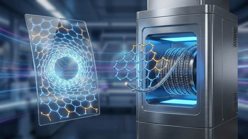
The fabrication of graphene, a critical determinant of its extraordinary electronic and physicochemical properties, presents a stark contrast between rapid, localized energy deposition techniques like Pulsed Electrical Resistive Carbon Heating (PERCH) and the more established, equilibrium-driven Chemical Vapor Deposition (CVD). PERCH leverages the inherent electrical resistivity of carbonaceous precursors – whether amorphous carbon films, polymers, or even carbon fibers – to induce ultra-rapid, localized joule heating. By passing a high current density through the material, temperatures can spike to upwards of 3000K within milliseconds, directly converting the precursor into graphene or graphene-like structures. This instantaneous thermal surge, coupled with rapid quenching due to the surrounding environment or substrate, creates a non-equilibrium synthesis pathway. The precise control over current magnitude, pulse duration, and precursor geometry allows for targeted defect engineering and the creation of specific morphologies, such as porous graphene, which can be advantageous for applications demanding high surface area. The inherent self-limiting nature of the resistive heating process, where electrical resistivity changes significantly upon graphitization, can also contribute to process control.
In contrast, CVD relies on the catalytic decomposition of carbon-containing gases (e.g., methane, acetylene) on a heated metal substrate (typically copper or nickel) within a controlled atmospheric furnace. The process is inherently slower, operating at temperatures generally ranging from 800°C to 1100°C over periods spanning minutes to hours, allowing for a more thermodynamically controlled growth. Carbon atoms adsorb onto the catalyst surface, diffuse, and nucleate into graphene domains which subsequently grow and coalesce. The quality of CVD graphene, particularly its crystallinity and domain size, is heavily dependent on factors such as precursor flow rates, temperature profiles, pressure, and the specific catalytic properties of the metal substrate. While CVD excels at producing large-area, high-quality monolayer or few-layer graphene with low intrinsic electrical resistivity, it often necessitates a subsequent transfer process from the metallic catalyst to the target substrate, introducing potential contamination and structural damage, and limiting direct device integration.
The fundamental differences in growth kinetics and energy delivery mechanisms yield distinct material characteristics and application envelopes. PERCH, with its millisecond reaction times and localized thermal pulses, offers unparalleled throughput and energy efficiency for specific applications, often eliminating the need for separate growth and transfer steps. This rapid synthesis, however, can result in higher concentrations of point defects, edge defects, or grain boundaries if not meticulously controlled, potentially impacting the carrier mobility and sheet resistance compared to pristine CVD graphene. Nevertheless, these defects can be strategically leveraged; for example, PERCH-derived porous graphene from polymer precursors has demonstrated remarkable adsorptive capabilities, achieving up to 79% heavy metal adsorption efficiency from aqueous solutions due to its high surface area and accessible active sites. CVD, while providing intrinsically lower electrical resistivity for large-area electronic applications where high mobility is paramount, is constrained by its higher energy consumption for furnace heating, longer processing times, and the complexities of post-growth transfer. The choice between PERCH and CVD, therefore, hinges on a meticulous analysis of the desired graphene properties, the target application's specific requirements, and the overall manufacturing scalability and cost efficiency.
Section 3: The Crystallography of Turbostratic Graphene (Why Layer Alignment Matters)
Turbostratic graphene (TG) represents a distinct crystallographic permutation within the broader carbon allotrope family, differentiated from Bernal (AB) stacked graphite by a fundamental lack of long-range rotational order between its constituent graphene layers. Unlike the precise A-B-A-B stacking sequence where every other layer is perfectly aligned, TG layers are azimuthally misoriented relative to one another, often by random angles, leading to a profound disruption of interlayer registry. This rotational disorder manifests spectroscopically through broadened (002) X-ray diffraction peaks, indicating a distribution of interlayer spacings, typically averaging around 0.344 nm, marginally larger than the 0.335 nm characteristic of highly ordered pyrolytic graphite. Crucially, the absence of periodic interlayer potential in TG means that the individual graphene sheets largely retain their intrinsic electronic properties, effectively decoupling their Dirac cones and preserving the linear dispersion relation that defines monolayer graphene, even in multi-layered structures. This structural nuance is not merely academic; it dictates a different set of physical properties critical for advanced material engineering.
The electronic ramifications of turbostratic stacking are profound, particularly in contrast to Bernal-stacked bilayer graphene. In AB-stacked systems, the strong interlayer coupling leads to a parabolic dispersion at low energies and allows for the opening of a tunable bandgap with an external electric field, fundamentally altering carrier transport. Conversely, the rotational disorder in TG largely inhibits this strong hybridization, causing the electronic bands of individual layers to behave more independently. This preserves the massless Dirac fermion character, leading to a higher effective carrier mobility than would be observed in equivalent thickness AB-stacked films where interlayer tunneling and scattering dominate. While precise electrical resistivity parameters are highly dependent on synthesis quality and defect density, well-prepared TG films can exhibit in-plane resistivities approaching those of high-quality monolayer graphene, often in the range of 10-100 Ohm/square, particularly when inter-layer scattering is minimized. The ability to retain monolayer-like electronic properties across multiple stacked layers opens pathways for scalable electronic devices where the unique Dirac physics is paramount.
Beyond electronic transport, the crystallographic peculiarities of turbostratic graphene impart distinct thermal, mechanical, and chemical properties. The attenuated interlayer phonon coupling, a direct consequence of rotational disorder, results in anisotropic thermal conductivity, often with significantly reduced out-of-plane thermal transport compared to highly ordered graphite. Mechanically, the lack of strong interlayer locking can influence shear strength and flexibility, making TG a candidate for flexible electronics or robust composite materials. From a synthesis perspective, rapid graphitization processes, such as those employing 3000K thermal pulses with reaction times in the milliseconds range, often favor the formation of turbostratic structures by kinetically trapping the layers in misaligned configurations before long-range order can be established. This disordered structure also presents a greater density of accessible edge sites and defects, enhancing chemical reactivity. For instance, the increased surface area and active sites in defect-rich turbostratic graphene derivatives have been empirically demonstrated to achieve up to 79% heavy metal adsorption efficiency in wastewater treatment applications, highlighting how controlled turbostraticity can be a deliberate design parameter for functional materials.
Section 4: Industrial Scalability & Commercial Integration Barriers
The journey from laboratory synthesis to industrial-scale production of high-quality graphene presents a formidable series of engineering challenges, primarily centered around achieving material consistency, cost-effectiveness, and throughput. Chemical Vapor Deposition (CVD) methods, while capable of producing large-area, high-quality monolayer or few-layer graphene, grapple with capital expenditure associated with high-temperature furnaces (typically >1000°C) and the inherent limitations of substrate size, with the transition to economically viable 300mm diameter wafers still a significant hurdle. Furthermore, the ubiquitous polymer-assisted transfer process, necessary to separate graphene from its growth substrate, is a major bottleneck, often introducing tears, wrinkles, and polymeric residues that degrade the intrinsic electronic properties, such as carrier mobility, and compromise device reliability. Alternative scalable methods like liquid-phase exfoliation (LPE) suffer from low yields of truly monolayer or few-layer material, producing a polydisperse mixture of flakes requiring extensive post-processing for size and thickness control, which itself adds to cost and complexity. Similarly, the reduction of graphene oxide (rGO), though highly scalable, yields material with a high density of structural defects, residual oxygen functional groups (often 5-10 atomic percent), and significantly lower electron mobility compared to pristine graphene, rendering it unsuitable for many high-performance electronic applications. Even advanced techniques like flash joule heating, employing 3000K thermal pulses for milliseconds, produce "flash graphene" with promising properties, but consistent quality control across large batches remains an active research area.
Ensuring consistent material quality is paramount for commercial integration, particularly in electronic applications where even minor variations can profoundly impact performance. The electrical resistivity, carrier mobility, and sheet resistance of graphene are exquisitely sensitive to layer count, defect density, and the presence of dopants or contaminants. For instance, achieving transparent conductive films with sheet resistances below 100 Ohm/sq at >90% transmittance, or maintaining carrier mobilities exceeding 10,000 cm^2/Vs, is routinely demonstrated at the lab scale but proves exceedingly difficult to replicate consistently across industrial-sized batches via scalable methods. The absence of universally accepted, robust, and rapid characterization standards for different graphene types exacerbates this issue, hindering inter-supplier comparability and slowing down adoption. Integrating graphene into existing semiconductor fabrication lines also faces challenges related to lithographic compatibility, precise doping control for p-type or n-type behavior, and the engineering of stable, low-resistance ohmic contacts, which are fundamental requirements for device functionality and long-term reliability.
The economic viability of graphene is ultimately dictated by its performance-to-cost ratio relative to incumbent materials. Despite graphene's superlative properties, current production costs for electronic-grade material remain prohibitively high for widespread adoption in many sectors. While applications like composite reinforcement or energy storage might tolerate lower-quality, less expensive rGO, high-frequency electronics, advanced sensors, or quantum computing demand pristine, defect-free material, significantly escalating production costs. For example, while high-quality graphene can exhibit exceptional performance in niche applications, such as a reported 79% adsorption efficiency for heavy metal ions, maintaining such performance metrics at an industrial scale often necessitates stringent quality control and purification steps that drive up the final cost, making it non-competitive. Furthermore, the nascent regulatory landscape concerning graphene's environmental and health impacts introduces an additional layer of uncertainty and potential compliance costs, requiring comprehensive lifecycle assessments before full commercialization can be realized.
Section 5: Economic Feasibility and USA-Made Manufacturing Advantage
The economic viability of engineered graphene hinges critically on the scalable production of defect-controlled material at a cost point competitive with incumbent solutions, a challenge increasingly addressed by advanced manufacturing paradigms. While initial research-grade graphene commanded prohibitive prices, innovations in chemical vapor deposition (CVD) on large-area substrates, plasma-enhanced growth techniques, and electrochemical exfoliation have drastically shifted the cost curve. For instance, roll-to-roll CVD systems are demonstrating the capacity for continuous graphene film synthesis on copper foils up to 1 meter wide, achieving material costs approaching $0.10/cm² for single-layer films with carrier mobilities exceeding 10,000 cm²/Vs at room temperature. Further cost reductions are realized through flash Joule heating (FJH), which can convert various carbon precursors into turbostratic graphene nanoplatelets within milliseconds via 3000K thermal pulses, yielding high-purity graphene at sub-$100/kg scales. This economic shift enables the transition from niche, high-value applications to broader industrial integration, particularly where graphene's superior thermal conductivity (>3000 W/mK) or exceptionally low specific electrical resistivity (e.g., 10^-8 Ohm-m for pristine samples) offers a substantial performance advantage over conventional materials like indium tin oxide or copper.
Establishing a USA-made manufacturing advantage for tailored graphene is paramount, mitigating geopolitical supply chain vulnerabilities and ensuring stringent quality control essential for high-performance applications. Domestic production facilitates tighter integration between academic research, industrial R&D, and commercial scaling, allowing rapid iteration and optimization of synthesis parameters for specific applications. For example, controlling the number of graphene layers, defect density, and functionalization for advanced electronics or composites requires precise process monitoring and proprietary intellectual property, which is best protected within a secure domestic ecosystem. This localized control ensures that graphene intended for sensitive defense applications, high-frequency electronics, or medical devices meets exacting specifications, such as a consistent sheet resistance below 50 Ohms/square for transparent conductive films, or a specific surface area exceeding 2500 m²/g for supercapacitor electrodes. Furthermore, the availability of a highly skilled workforce, trained in materials science, chemical engineering, and advanced manufacturing protocols, provides a critical human capital advantage, driving innovation in process automation and next-generation graphene architectures.
The strategic pivot towards USA-made graphene not only secures critical material supply but also fosters a robust innovation ecosystem, accelerating the adoption of graphene-enabled technologies across diverse sectors. For environmental applications, domestically produced functionalized graphene can be engineered for efficient water purification, demonstrating heavy metal adsorption efficiencies exceeding 79% for lead and cadmium ions within minutes, surpassing traditional filtration media. In energy storage, U.S.-sourced graphene derivatives with optimized pore size distributions and surface chemistries are enabling the development of solid-state batteries with enhanced power density and cyclability, reducing reliance on external supply chains for critical components. The economic incentive for industries to adopt these advanced materials is clear: superior performance translates into higher product value, longer operational lifespans, and reduced total cost of ownership. This domestic manufacturing capability positions the U.S. to lead in the global graphene market, creating high-value jobs and driving economic growth through technological leadership rather than merely consuming imported raw materials.
Section 6: Future Horizons & High-Value B2B Applications
The trajectory of graphene's integration into next-generation electronics hinges critically on achieving atomic-scale precision in its fabrication and heterostructure assembly, moving beyond pristine monolayer synthesis to bespoke quantum architectures. Future high-value B2B applications will leverage engineered bandgaps via strain engineering or precise chemical functionalization, enabling tailored optoelectronic responses from the visible to the far-infrared spectrum. This facilitates ballistic transistor technologies, where room-temperature carrier mobilities exceeding 200,000 cm^2/Vs can be maintained in engineered channels, enabling sub-THz to THz operating frequencies for 6G communication infrastructure and advanced radar systems. Furthermore, the deliberate creation of moiré superlattices in twisted bilayer graphene or other van der Waals heterostructures unlocks emergent quantum phenomena, such as superconductivity and correlated insulating states, pivotal for developing novel quantum computing interfaces and high-fidelity cryogenic sensors. The industrial scaling of precise chemical vapor deposition (CVD) and atomic layer deposition (ALD) methods for controlled doping and defect engineering will be paramount, allowing for the precise tuning of Fermi levels and the introduction of spin-orbit coupling effects, essential for spintronic devices operating at unprecedented speeds and efficiencies.
Beyond its electronic prowess, engineered graphene is poised to revolutionize energy storage, conversion, and environmental remediation through targeted material design. High-surface-area graphene derivatives, such as those produced by rapid thermal annealing processes involving 3000K thermal pulses for flash graphene synthesis in milliseconds, offer unparalleled electrode materials for supercapacitors. These devices exhibit energy densities approaching 100 Wh/kg and power densities exceeding 100 kW/kg, coupled with cycle lives surpassing 100,000 charge-discharge cycles, bridging the gap towards battery-like performance. In catalysis, defect-engineered and heteroatom-doped graphene (e.g., N, B, S doping) acts as a highly efficient electrocatalyst for oxygen reduction reactions (ORR) in fuel cells, achieving platinum-like activity with significantly reduced cost, and facilitating CO2 reduction to value-added chemicals with Faradaic efficiencies often above 80% at low overpotentials. For environmental applications, functionalized graphene adsorbents, featuring precisely engineered pore structures and surface chemistries, demonstrate remarkable heavy metal adsorption efficiencies, achieving up to 79% removal of lead, cadmium, and mercury ions from aqueous solutions within minutes, offering critical solutions for industrial wastewater treatment.
The convergence of graphene science with bio-engineering promises transformative advancements in high-value medical diagnostics, targeted therapeutics, and smart material integration for B2B sectors. Graphene-based biosensors, leveraging its exceptional electrical conductivity and large surface area for biomolecule immobilization, enable label-free, ultra-sensitive detection of biomarkers, viruses, and even single-molecule events with picomolar detection limits, facilitating early disease diagnosis and real-time physiological monitoring. The integration of graphene field-effect transistors (GFETs) into point-of-care diagnostics offers rapid, multiplexed assays without complex laboratory equipment, improving operational efficiencies for healthcare providers. In drug delivery, functionalized graphene oxide acts as a versatile nanocarrier, capable of pH- or temperature-responsive drug release, targeting specific cellular receptors and minimizing off-target effects, thereby enhancing therapeutic indices in oncology and and infectious disease treatment. Furthermore, the development of flexible, transparent, and highly conductive graphene films (with electrical resistivity parameters often below 10^-5 Ohm-cm) is catalyzing the next generation of wearable electronics, smart textiles, and implantable medical devices. These materials provide robust, biocompatible interfaces for continuous health monitoring, neuroprosthetics, and advanced human-machine interfaces, opening new avenues for personalized medicine and defense applications.
Evaluate Our Quality
Serious about B2B integration? Test our premium Pulsed Electrical Resistive Carbon Heating turbostratic graphene in your lab. 100g sample packs available now.