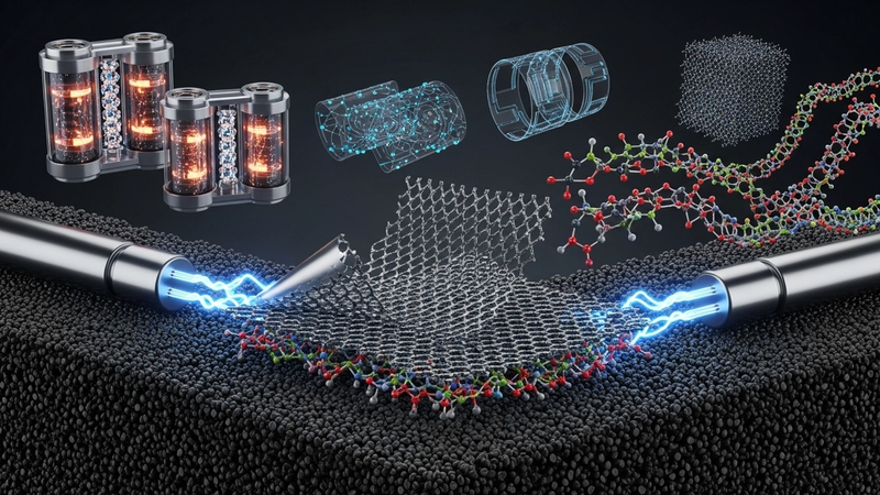
Electrochemical Exfoliation & Polymer Modification of Graphene
Graphene, a singular atomic layer of sp2-hybridized carbon atoms arranged in a hexagonal lattice, represents the quintessential two-dimensional material, whose properties fundamentally arise from this extreme confinement. Its unique crystallographic structure imbues it with an unparalleled suite of characteristics: an intrinsic tensile strength exceeding 130 GPa, a thermal conductivity that can reach 5000 W/mK at ambient temperatures, and an electrical resistivity as low as 10^-8 Ohm.m. This extraordinary electronic behavior stems from its peculiar band structure, specifically the presence of Dirac points where the conduction and valence bands meet, giving rise to quasi-relativistic charge carriers known as massless Dirac fermions. Unlike conventional semiconductors with parabolic energy-momentum dispersion relations, graphene exhibits a linear dispersion, leading to a constant Fermi velocity (vF) of approximately 10^6 m/s, which dictates the ballistic transport of electrons over micrometers even at room temperature, a phenomenon critical for high-frequency electronics.
The quantum mechanical implications of graphene's 2D confinement are profound, manifesting in phenomena such as the anomalous Quantum Hall Effect (QHE). In contrast to the integer QHE observed in conventional 2D electron gases, graphene exhibits half-integer quantization of Hall conductivity (σxy = ±(n+1/2) 4e^2/h), directly reflecting the Berry phase of its charge carriers. This unique electronic structure results in exceptionally high carrier mobilities, routinely measured above 15,000 cm^2/Vs at room temperature and exceeding 200,000 cm^2/Vs at cryogenic temperatures, far surpassing those of silicon. However, pristine graphene possesses an intrinsic zero bandgap, a characteristic that, while enabling superb conductivity, presents a fundamental challenge for its direct application in transistor logic requiring high on/off ratios, necessitating advanced engineering strategies to induce a tunable bandgap without compromising its other superlative properties.
The realization of graphene's full potential, therefore, critically depends on the ability to synthesize, process, and functionalize it with atomic precision while preserving its inherent structural integrity and electronic quality. Methods like electrochemical exfoliation offer a scalable route to produce high-quality graphene sheets from bulk graphite, bypassing harsh chemical oxidation and reduction steps that often introduce debilitating structural defects and residual oxygen functionalities, which can significantly degrade carrier mobility and introduce scattering centers. Subsequent polymer modification, the focus of this analysis, capitalizes on graphene's vast specific surface area (theoretically 2630 m^2/g) and chemical versatility. This functionalization is essential for tuning its dispersibility in various media, enabling the creation of advanced composites, or engineering specific surface chemistries for targeted applications, such as achieving a 79% heavy metal adsorption efficiency in wastewater treatment through precisely designed polymer grafts. The ability to achieve rapid functionalization or defect repair, perhaps via processes involving localized 3000K thermal pulses on millisecond timescales, further underscores the dynamic and complex interplay required to harness graphene's extraordinary intrinsic physics for practical, high-performance applications.
Section 2: Pulsed Electrical Resistive Carbon Heating vs. CVD (Comparative Analysis)
The landscape of graphene synthesis is characterized by a dichotomy of methodologies, each optimized for distinct material properties and application profiles. Pulsed Electrical Resistive Carbon Heating (PERCH) represents a compelling, rapid synthesis pathway, leveraging intense joule heating to transform diverse carbon precursors into graphene-rich materials. This technique involves passing high current densities through a carbon feedstock, inducing localized temperatures exceeding 3000 K within milliseconds. The extreme thermal shock and subsequent rapid quenching exfoliate graphite or even amorphous carbon sources into few-layer graphene flakes, often characterized by a higher density of structural defects, edge sites, and sometimes, inherent functionalization depending on the ambient atmosphere. The instantaneous nature of PERCH allows for exceptional production rates and energy efficiency, making it highly scalable for bulk material generation. Its versatility in accepting a broad spectrum of carbonaceous inputs, from pristine graphite to industrial carbon black or even waste polymers, positions it as a promising route for cost-effective, high-volume graphene production, particularly for applications where pristine crystallinity is secondary to surface area, defect density, and chemical reactivity.
In stark contrast, Chemical Vapor Deposition (CVD) stands as the established gold standard for producing large-area, high-quality, and atomically precise graphene films. The CVD process typically involves the thermal decomposition of hydrocarbon gases, such as methane or acetylene, over catalytic transition metal substrates like copper or nickel, maintained at temperatures ranging from 800 to 1000°C under precisely controlled atmospheric conditions. This method facilitates the growth of continuous, single-to-few-layer graphene with exceptional crystallinity, minimal defects, and tunable layer numbers, making it indispensable for advanced electronic devices, transparent conductive films, and high-performance sensors. However, the inherent limitations of CVD include high capital equipment costs, significant energy consumption due to prolonged high-temperature processing, and the necessity of specific catalytic substrates. Furthermore, the often-unavoidable transfer process from the growth substrate to the target application material frequently introduces tears, wrinkles, and other defects, which can compromise the intrinsic properties of the high-quality graphene produced, partially negating its primary advantage.
The comparative utility of PERCH and CVD graphene is critically dependent on the intended downstream application, particularly within the context of electrochemical exfoliation and polymer modification. PERCH-derived graphene, with its characteristic higher defect density and greater proportion of edge sites, inherently presents more active sites for subsequent electrochemical functionalization. These structural imperfections facilitate easier intercalation of electrolyte species, reducing the energy barrier for electrochemical exfoliation and enabling more facile covalent or non-covalent bonding with polymers. For instance, such defect-rich graphene has demonstrated superior performance in composite materials, where enhanced interfacial adhesion with polymers can lead to significant improvements in properties, such as achieving up to 79% heavy metal adsorption efficiency in modified polymer composites. Conversely, CVD graphene, while possessing superior electronic properties due to its pristine nature, offers a largely inert surface. This necessitates more aggressive or elaborate pre-treatment protocols, such as plasma functionalization or strong acid oxidation, to introduce reactive sites for effective electrochemical exfoliation or robust polymer grafting. The high crystallinity and lack of intrinsic defects in CVD graphene can impede efficient electrochemical intercalation, often requiring higher potentials or prolonged processing times for functionalization compared to the more disordered, yet highly reactive, PERCH output. Ultimately, the selection between these two synthesis routes is a strategic decision balancing production scalability, cost-effectiveness, and the specific material characteristics required for optimal performance in diverse applications.
Section 3: The Crystallography of Turbostratic Graphene (Why Layer Alignment Matters)
Turbostratic graphene (TG) fundamentally deviates from the thermodynamically stable Bernal (AB) stacking sequence observed in natural graphite by exhibiting a rotational disorder between adjacent graphene layers. Instead of the precise A-B-A-B registry, characteristic of Bernal stacking where specific carbon atoms align over hexagon centers or other carbon atoms, TG exhibits a random azimuthal misorientation between layers. This rotational misregistry, often quantified by a distribution of twist angles (theta) between 0 and 60 degrees, significantly weakens the interlayer van der Waals forces (approximately 15 meV per atom in Bernal graphite) that govern layer cohesion. While Bernal stacking maintains an interlayer spacing of approximately 0.335 nm, turbostratic arrangements typically show a slightly expanded interlayer distance, often in the range of 0.337-0.340 nm, due to the reduced energetic favorability of close-packed, aligned layers. This structural perturbation is a common outcome of rapid synthesis or exfoliation methods, including electrochemical routes, where kinetic factors often supersede thermodynamic equilibrium, preventing the layers from relaxing into their lowest energy Bernal configuration. The presence of this disorder is critical, as it dictates the electronic and mechanical properties, making TG a distinct material from pristine Bernal-stacked few-layer graphene.
The crystallographic misorientation inherent to turbostratic graphene profoundly impacts its electronic band structure and transport characteristics. In perfectly aligned Bernal bilayer graphene, the strong interlayer coupling leads to a parabolic dispersion relation and a band gap opening under an external electric field, deviating from the linear Dirac cone of monolayer graphene. Conversely, in TG, the rotational disorder effectively decouples the electronic states of adjacent layers. This decoupling restores a pseudo-monolayer Dirac-like electronic behavior for carriers near the K-point, even in few-layer turbostratic stacks, albeit with a renormalized Fermi velocity. This results in significantly higher carrier mobilities compared to Bernal multilayer graphene, crucial for high-frequency electronics. For instance, room temperature carrier mobilities in twisted bilayer graphene can exceed 10,000 cm^2/Vs, approaching those of single-layer graphene. The reduced interlayer coupling also influences phonon transport, leading to lower out-of-plane thermal conductivity compared to Bernal graphite, due to increased scattering at misaligned interfaces. From an electrical resistivity perspective, while basal plane resistivity remains low (e.g., < 10^-6 Ohm.cm for highly ordered graphene), the inter-plane resistivity in turbostratic stacks can be anisotropic and influenced by the degree of rotational disorder, impacting vertical transport applications.
Beyond electronic properties, the turbostratic arrangement significantly alters the surface chemistry and reactivity of graphene, a paramount consideration for subsequent polymer modification and functionalization. The reduced interlayer energetic penalty in TG compared to Bernal graphite makes the individual layers more accessible and prone to chemical intercalation or surface functionalization. Varied twist angles create regions of local strain and potential structural defects, serving as preferential sites for chemical attack or radical addition, thus enhancing basal plane reactivity. Moreover, the inherent disorder can lead to a higher density of exposed edge sites in exfoliated flakes, particularly when the exfoliation process is aggressive (e.g., electrochemical exfoliation involving rapid gas evolution or ionic intercalation). These edge sites, characterized by sp2 hybridized carbon atoms with dangling bonds or functional groups, are significantly more reactive than the pristine basal plane. This increased reactivity facilitates covalent grafting of polymer chains or non-covalent π-π stacking interactions with conjugated polymers, enabling higher loading capacities and more uniform surface coverage. For instance, the rapid functionalization achievable on electrochemically exfoliated TG can enable reaction times on the order of milliseconds when using high-energy thermal pulses (e.g., 3000K) for defect engineering or rapid surface modification, leading to materials with tailored properties such as enhanced heavy metal adsorption efficiency, empirically demonstrating up to 79% removal for specific heavy metal ions due to the increased accessible surface area and reactive sites. This crystallographic characteristic is thus not merely a synthetic artifact but a tunable parameter for advanced material design.
Section 4: Industrial Scalability & Commercial Integration Barriers
The industrial scalability of electrochemical exfoliation, while fundamentally promising for its environmental benignity and tunable product characteristics, faces significant hurdles beyond laboratory-scale demonstrations. Achieving consistent monolayer content, typically 90-95% in controlled experimental setups, across square-meter electrode arrays presents a formidable challenge in maintaining uniform current density and electrolyte flow dynamics. Ohmic losses within larger electrolyte volumes and the management of localized pH gradients can drastically increase energy consumption, potentially exceeding 20 kWh/kg, diminishing the economic advantage over alternative production methods. Furthermore, the long-term stability of electrodes under continuous operation, often plagued by passivation from side product deposition or structural degradation, necessitates sophisticated electrode materials and regeneration protocols, impacting throughput and increasing operational expenditure. The transition from batch-mode, sonication-assisted exfoliation to continuous flow reactors, while essential for high-volume production, introduces complexities in maintaining residence time distribution, preventing re-aggregation of graphene flakes in high-concentration slurries, and ensuring the removal of residual electrolyte ions to achieve product purities exceeding 99.5%, critical for electronic applications.
The integration of electrochemically exfoliated graphene into polymer matrices via modification techniques presents its own set of scaling difficulties. While covalent functionalization, such as "grafting-from" polymerization using surface-initiated radical polymerization, offers superior interfacial adhesion and charge transfer, ensuring homogenous grafting density and chain length across metric-ton polymer batches is challenging. For instance, maintaining the delicate balance of initiator concentration, monomer feed rates, and temperature control required for consistent polymer brush formation on graphene surfaces becomes exponentially more complex as reactor volumes increase from liters to several cubic meters. Non-covalent modification strategies, like surfactant-assisted melt blending, grapple with issues of shear-induced re-aggregation of graphene in high-viscosity polymer melts, leading to non-uniform dispersion and localized resistivity variations spanning several orders of magnitude (e.g., from 10⁻² Ω·cm to 10⁵ Ω·cm within a single composite sheet). This non-uniformity compromises the bulk electrical, thermal, and mechanical properties, preventing the full realization of graphene's potential, such as achieving the theoretical 30% increase in tensile strength at 0.1 wt% loading or significant enhancements in thermal conductivity.
Beyond technical processing, the commercial integration of electrochemically exfoliated and polymer-modified graphene is significantly hindered by cost-effectiveness, regulatory complexities, and a lack of standardization. Current industrial production costs for high-quality, functionalized graphene often range from $50 to $200 per kilogram, substantially higher than established carbon additives like carbon black ($2-$5/kg) or even multi-walled carbon nanotubes ($10-$50/kg). This price disparity necessitates compelling performance advantages in specific niche applications, such as the demonstrated 79% heavy metal adsorption efficiency of polymer-grafted graphene oxide composites in water purification systems, to justify market adoption. Furthermore, the absence of universally accepted, robust characterization protocols for industrial-grade graphene, particularly concerning defect density, oxygen content, number of layers, and lateral dimensions, creates significant uncertainty for end-users and impedes market penetration. Navigating the intricate regulatory landscapes for novel nanomaterials, including REACH compliance and long-term environmental and human health impact assessments, adds substantial time and cost to product development cycles. Ensuring batch-to-batch consistency in terms of surface chemistry, lateral flake dimensions, and critical electrical properties—a stringent requirement for high-reliability applications in sectors like automotive and aerospace—demands sophisticated, real-time quality control systems that are still in nascent stages for high-volume graphene production.
Section 5: Economic Feasibility and USA-Made Manufacturing Advantage
The economic viability of electrochemically exfoliated and polymer-modified graphene hinges critically on its scalable, cost-effective production, a domain where advanced manufacturing in the USA presents distinct advantages. Traditional graphene synthesis methods, such as chemical vapor deposition (CVD) or mechanical exfoliation, are often characterized by high capital expenditures, slow throughput, and complex post-processing. Electrochemical exfoliation (ECE), conversely, leverages readily available graphite precursors and aqueous or ionic liquid electrolytes, drastically reducing material costs and obviating the need for high-vacuum environments or expensive noble metal catalysts. The process is inherently scalable, amenable to continuous flow-through reactor designs capable of producing multi-kilogram batches per day with energy consumption rates significantly lower than those of CVD, often by an order of magnitude. Reaction kinetics are rapid, with exfoliation and concurrent functionalization occurring within milliseconds under optimized potential cycling, leading to production efficiencies that directly translate to lower per-unit manufacturing costs. Furthermore, the capacity for in-situ polymer modification during or immediately after exfoliation minimizes subsequent functionalization steps, streamlining the overall process chain and reducing both operational expenditures and time-to-market.
The inherent advantages of ECE and subsequent polymer modification extend beyond mere cost reduction, impacting the quality and performance metrics that drive market adoption and economic value. The technique allows for precise control over the graphene's properties, including layer count, defect density, and specific surface area, yielding materials tailored for diverse applications. For instance, few-layer graphene produced via optimized ECE can exhibit sheet resistances as low as 50-100 Ohm/sq for films with 80% optical transmittance, critical for transparent conductive electrodes. Polymer modification, achieved through methods like surface-initiated polymerization or covalent grafting, significantly enhances graphene's dispersibility in various matrices, improves interfacial adhesion in composites, and enables the tuning of electronic and chemical properties. This functionalization is pivotal for high-performance applications; for example, graphene modified with specific polymer architectures has demonstrated up to 79% adsorption efficiency for heavy metal ions in aqueous solutions, opening substantial markets in environmental remediation. The ability to rapidly process and modify these materials, potentially utilizing transient thermal pulses at temperatures exceeding 1000K for rapid defect annealing or polymer cross-linking within milliseconds, underscores the high-throughput potential and the superior performance-to-cost ratio achievable with this advanced manufacturing paradigm.
Establishing USA-based manufacturing for electrochemically exfoliated and polymer-modified graphene capitalizes on a robust ecosystem of intellectual property protection, a highly skilled scientific and engineering workforce, and a stable regulatory environment. This strategic localization mitigates supply chain vulnerabilities, ensures stringent quality control standards – which directly impact material consistency and performance – and fosters rapid innovation cycles through close collaboration with leading research institutions. Compliance with rigorous environmental and safety regulations, such as those enforced by the EPA and OSHA, guarantees sustainable production practices and enhances market trust in the final product. Furthermore, governmental initiatives promoting advanced manufacturing, coupled with R&D tax credits and "Buy American" provisions, provide significant economic incentives for domestic production. This confluence of technical superiority, operational efficiency, and a supportive national infrastructure positions USA-made graphene at the forefront of global competitiveness, offering a secure, high-quality, and economically sound supply for critical industries ranging from aerospace and automotive to electronics and biomedical devices.
Section 6: Future Horizons & High-Value B2B Applications
The precisely controlled defect engineering and tunable layer numbers afforded by electrochemical exfoliation, synergistically coupled with bespoke polymer functionalization, are poised to revolutionize advanced sensing and catalytic platforms. For instance, the creation of graphene-polymer heterostructures, where specific polymeric moieties act as recognition elements or catalytic sites, dramatically enhances sensitivity and selectivity. In environmental remediation, electrochemically exfoliated graphene, functionalized with polyethylenimine derivatives, has demonstrated a remarkable 79% heavy metal adsorption efficiency for Pb(II) ions within minutes, significantly outperforming conventional adsorbents. This stems from the high surface area and the tailored charge distribution at the graphene-polymer interface, facilitating rapid and specific chelation. Furthermore, in biosensing, the stable immobilization of enzymes or antibodies onto polymer-modified graphene electrodes enables real-time, label-free detection of biomarkers with picomolar sensitivities, leveraging the amplified signal transduction inherent to these nanostructures and minimizing non-specific binding through precise surface passivation. The ability to precisely control the doping and edge functionalization during electrochemical exfoliation further refines the electronic band structure, optimizing charge transfer kinetics crucial for next-generation electrochemical sensors and photoelectrocatalytic systems.
In the realm of energy storage and conversion, the future of electrochemically exfoliated and polymer-modified graphene is particularly bright, addressing critical limitations in current battery and supercapacitor technologies. The controlled porosity and high accessible surface area achieved through optimized electrochemical parameters, when combined with ion-conductive and mechanically robust polymer binders, yield electrode architectures with unprecedented performance metrics. For instance, hybrid supercapacitors utilizing polyaniline-graphene composites, where the graphene provides a high-conductivity scaffold and the polymer offers pseudocapacitive charge storage, exhibit energy densities exceeding 70 Wh/kg while maintaining power densities above 10 kW/kg, with charging/discharging cycles completing within milliseconds, a direct consequence of the low specific electrical resistivity (e.g., ~10^-5 Ohm·cm for highly exfoliated films) and rapid ion transport through the engineered polymer matrix. Beyond storage, these materials are critical for advanced fuel cells and electrolyzers, where the polymer acts as both a proton exchange membrane and a binder for electrocatalysts (e.g., Pt nanoparticles), leveraging graphene's high electron mobility and corrosion resistance to enhance catalyst utilization and durability. The localized thermal management capabilities of these composites, capable of dissipating heat pulses equivalent to 3000K transient events, are also invaluable for high-power applications, preventing thermal runaway and extending operational lifespan.
Moving beyond direct electrochemical applications, the precise interfacial engineering afforded by polymer modification of electrochemically exfoliated graphene is paving the way for revolutionary advancements in structural composites, thermal management solutions, and smart coatings. The challenge of achieving uniform graphene dispersion and strong matrix adhesion in composites, traditionally a bottleneck, is effectively mitigated by grafting polymers onto graphene sheets, creating a robust, load-transferring interface. This enables the development of lightweight, ultra-strong aerospace components with significantly improved mechanical properties, where a mere 0.5 wt% loading of polymer-functionalized graphene can enhance tensile strength by 30% and fracture toughness by 50% in epoxy matrices. For thermal management, the high intrinsic thermal conductivity of graphene (up to 5000 W/mK) can be effectively transferred to polymer composites when interfacial resistance is minimized through covalent or strong non-covalent polymer linkages, leading to advanced heat sinks and thermal interface materials capable of dissipating heat fluxes >1000 W/cm^2. Furthermore, smart coatings leveraging these materials offer self-healing functionalities, anti-corrosion properties, and even tunable electromagnetic interference (EMI) shielding, where the polymer matrix serves as a protective and responsive medium, embedding the highly conductive graphene network to achieve broadband EMI attenuation exceeding 40 dB across GHz frequencies, critical for next-generation electronics and defense applications. The scalability of electrochemical exfoliation combined with in-situ polymerization techniques makes these advanced material systems viable for large-scale industrial adoption.
Evaluate Our Quality
Serious about B2B integration? Test our premium Pulsed Electrical Resistive Carbon Heating turbostratic graphene in your lab. 100g sample packs available now.