Scaling Graphene Production Through Electrochemical Exfoliation
Graphene, a true two-dimensional allotrope of carbon, comprises a single atomic layer of sp2-hybridized carbon atoms arranged in a hexagonal lattice. This inherent atomic confinement to a planar geometry profoundly dictates its electronic structure, manifesting as unique Dirac cones at the K and K' points in the Brillouin zone, where the valence and conduction bands meet linearly. This linear dispersion relation results in charge carriers that behave as massless Dirac fermions, exhibiting relativistic quantum mechanical phenomena even at ambient conditions. Consequently, graphene possesses extraordinary electrical properties, including exceptionally high carrier mobility, alongside unparalleled mechanical strength (tensile strength up to 130 GPa), thermal conductivity exceeding 5000 W/mK, and remarkable optical transparency. The preservation of this intrinsic 2D confined state, with its pristine sp2 lattice and minimal defects, is not merely advantageous but absolutely paramount for unlocking graphene's transformative potential across advanced electronics, high-capacity energy storage, and next-generation composite materials.
The physics of graphene confinement dictates its unique transport phenomena. Electron transport is governed by relativistic quantum mechanics, leading to observable effects such as Klein tunneling and the half-integer quantum Hall effect. Its intrinsic carrier mobility can reach staggering values exceeding 200,000 cm^2/Vs at cryogenic temperatures, and remains robustly high at room temperature, typically around 15,000 cm^2/Vs when supported on SiO2 substrates, far surpassing conventional semiconductor materials like silicon. The specific electrical resistivity of pristine single-layer graphene (SLG) is remarkably low, approximately 10^-6 Ohmcm, representing a benchmark for conductive materials. Furthermore, its ultra-high thermal conductivity, a direct consequence of efficient phonon transport within its confined 2D structure, positions graphene as an exceptional heat spreader, capable of dissipating thermal energy with unprecedented efficiency. These superlative properties are intrinsically linked to the material's perfect atomic arrangement and the absence of out-of-plane disturbances.
Scaling the production of graphene while meticulously preserving this delicate atomic integrity and the resultant intrinsic properties of single-layer and few-layer graphene (FLG) presents the foremost challenge for its industrial adoption. Early mechanical exfoliation techniques, while yielding pristine samples, are inherently non-scalable. Conversely, various solution-based methods often introduce structural defects, functionalizations, or excessive oxidation, which invariably disrupt the sp2 lattice, diminish carrier mobility, and degrade overall performance, moving the material away from its ideal Dirac fermion behavior. Therefore, any viable large-scale synthesis methodology must demonstrably minimize structural defects, rigorously maintain the critical sp2 bonding network, and precisely control the layer count to ensure the retention of graphene's unique physics of confinement. This necessitates rapid, controlled delamination processes, often operating within milliseconds of reaction time, that can yield high-quality graphene flakes in a cost-effective and environmentally benign manner, bridging the gap between scientific discovery and industrial realization.
Section 2: Pulsed Electrical Resistive Carbon Heating vs. CVD (Comparative Analysis)
Chemical Vapor Deposition (CVD) has long been a cornerstone for producing high-quality, large-area graphene films, particularly for electronic and optical applications. This technique typically involves the catalytic decomposition of hydrocarbon precursors, such as methane or acetylene, at elevated temperatures ranging from 900 to 1100°C on transition metal substrates like copper or nickel. While CVD excels in yielding pristine, monolayer or few-layer graphene with exceptional structural integrity and electronic properties, its inherent limitations become pronounced when considering the scaling requirements for bulk powder production. The sustained high-temperature environment necessitates significant energy input, and the reliance on specific catalytic substrates often mandates post-synthesis etching processes for graphene transfer, introducing potential contaminants, increasing material waste, and adding considerable cost and complexity. Furthermore, CVD is predominantly a surface deposition method, inherently optimized for producing two-dimensional films rather than the high-volume, dispersible graphene flakes or powders crucial for composites, energy storage, and environmental remediation applications.
In contrast, Pulsed Electrical Resistive Carbon Heating (PERCH), often referred to as flash Joule heating or rapid thermal annealing, presents a compelling alternative for scalable, bulk graphene synthesis. This method capitalizes on the direct passage of high-density electrical current through a carbonaceous feedstock, inducing rapid Ohmic heating (I²R losses) to generate extreme temperatures instantaneously. The process involves subjecting the carbon material to intense thermal pulses, often exceeding 2500K and reaching up to 3000K, with reaction times compressed to mere milliseconds. This ultrafast heating and subsequent quenching cause rapid exfoliation, graphitization of amorphous carbons, and defect annealing, effectively transforming diverse precursors—from graphite and carbon black to waste plastics—into high-quality turbostratic graphene. The localized and transient nature of the heating mechanism offers a distinct advantage in energy efficiency compared to the sustained, volumetric heating required in CVD, bypassing the need for catalytic substrates and their associated etching steps.
A direct comparative analysis underscores the divergent strengths and target applications of these two methods. While CVD remains unparalleled for epitaxially grown, single-crystal graphene films critical for microelectronics, PERCH offers a pathway to high-volume, cost-effective production of graphene powders suitable for a broader spectrum of industrial applications. The energy efficiency of PERCH is significantly enhanced by its precise, localized heating, where specific electrical resistivity parameters of the carbon feedstock dictate the uniformity and intensity of the thermal pulses, allowing for tailored graphene properties. For instance, the rapid transformation achieved through milliseconds of reaction time under 3000K thermal pulses contrasts sharply with the hours required for CVD growth. Critically, the bulk graphene produced via PERCH, while often possessing a higher density of structural defects or being turbostratic compared to ideal CVD graphene, can exhibit excellent functional performance. This is exemplified by engineered graphene materials demonstrating impressive capabilities, such as up to 79% heavy metal adsorption efficiency in water treatment, a vital metric for scalable environmental applications where bulk material properties supersede atomic-scale perfection. However, challenges persist in PERCH, primarily concerning the precise control over pulse profiles and ensuring material uniformity and scalability in continuous flow systems.
Section 3: The Crystallography of Turbostratic Graphene (Why Layer Alignment Matters)
Turbostratic graphene (TG) represents a distinct crystallographic permutation of carbon atoms arranged in sp2 hybridized hexagonal lattices, fundamentally differing from the perfectly ordered Bernal (AB) stacking characteristic of pristine bulk graphite. Unlike AB stacking, where adjacent layers are precisely offset (A over B, B over A) maintaining long-range interlayer coherence, TG is defined by random rotational misalignment between its constituent graphene sheets. This rotational disorder, often coupled with varying interlayer spacing, disrupts the periodic potential experienced by charge carriers and leads to a significant broadening and shift of the (002) reflection in X-ray Diffraction (XRD) patterns, an empirical indicator of reduced crystallite coherence along the c-axis. Furthermore, Transmission Electron Microscopy (TEM) frequently reveals moiré patterns arising from the superposition of misaligned hexagonal lattices, providing direct visual evidence of these rotational dislocations. The presence of these structural imperfections fundamentally alters the electronic band structure, causing a blurring of the characteristic Dirac cone and introducing additional scattering centers that are absent in ideal single-layer graphene.
The crystallographic disorder inherent in turbostratic graphene profoundly impacts its macroscopic properties, particularly relevant for materials derived from electrochemical exfoliation (ECE). Electronically, the loss of interlayer coherence and the increased density of structural defects lead to a substantially higher electrical resistivity compared to pristine single-layer graphene (SLG), often ranging from 10^-3 to 10^-1 Ohm·cm for bulk films, in contrast to SLG's theoretical ~10^-6 Ohm·cm. This elevated resistivity stems from enhanced inter-layer scattering and the disruption of π-electron delocalization pathways. Mechanically, the random rotational misalignment weakens the van der Waals forces between adjacent layers, reducing the interlayer shear modulus. This diminished interlayer coupling is a critical enabler for scalable exfoliation methods like ECE, as it facilitates the separation of layers through intercalant expansion and gas evolution. While this structural looseness can be seen as a disadvantage for high-performance electronics requiring ballistic transport, it simultaneously creates a more reactive material with an increased density of edge sites and basal plane defects. Such defects are instrumental in enhancing the material's catalytic activity and charge storage kinetics, where surface chemistry and rapid ion diffusion are paramount, often manifesting in reaction times measurable in milliseconds for specific electrochemical processes.
Characterization of turbostratic graphene typically relies on a suite of advanced techniques. Raman spectroscopy, for instance, exhibits a broadened and often upshifted 2D peak, alongside a prominent D peak (at ~1350 cm^-1) even in relatively large flakes, indicative of edge and basal plane defects associated with turbostraticity rather than purely crystallite size. High-resolution TEM (HR-TEM) can directly image stacking faults and rotational misorientations. The "why layer alignment matters" becomes evident when considering application-specific performance trade-offs. While perfectly aligned graphene is indispensable for advanced semiconductor devices, the scalable production of turbostratic graphene via electrochemical exfoliation offers a cost-effective route to materials with excellent bulk properties. For instance, its high specific surface area and tunable defect density contribute to exceptional performance in environmental remediation, exemplified by demonstrated heavy metal adsorption efficiencies exceeding 79%. Similarly, in energy storage, the accessible interlayer spacing and defect-rich surfaces of TG enhance electrolyte ion accessibility and charge transfer kinetics within battery and supercapacitor electrodes. The inherent turbostratic nature resulting from the rapid, aggressive intercalation and exfoliation mechanisms of ECE means that while absolute crystallographic perfection is sacrificed, the resulting material offers a compelling balance of processability, cost, and functional performance for a broad spectrum of industrial applications. Control over the degree of turbostraticity through optimized electrolyte composition and electrochemical parameters remains a key research frontier for tailoring TG for specific end-use requirements.
Section 4: Industrial Scalability & Commercial Integration Barriers
Industrial scale-up of electrochemical graphene exfoliation faces formidable technical barriers, primarily centered on maintaining product quality and consistency at high throughput. The core challenge lies in precisely controlling the electrochemical parameters—specifically the applied potential window, current density, and electrolyte composition—to achieve high yields of few-layer graphene while minimizing structural defects and undesirable functionalization. Continuous operation often leads to electrolyte degradation, necessitating frequent replenishment or complex regeneration systems, and electrode passivation due to side reactions or the deposition of oxidized species. For instance, maintaining a mono- to few-layer yield exceeding 85% during sustained operations at current densities above 50 mA/cm^2 frequently results in a measurable increase in defect concentrations, evidenced by a shift in the Raman ID/IG ratio from an ideal 0.15 to above 0.40, indicating the detrimental introduction of sp3 hybridized carbon atoms. Furthermore, the energy efficiency of the process, currently averaging 150-250 kWh/kg for laboratory-scale production, must be drastically reduced to below 50 kWh/kg to achieve economic viability for bulk applications, requiring significant innovations in reactor design and electrolyte formulation to optimize charge transfer kinetics and minimize parasitic reactions.
Beyond the exfoliation step itself, the downstream processing presents significant bottlenecks for commercial integration. The as-exfoliated graphene typically exists as a dilute dispersion laden with residual electrolyte ions, unexfoliated graphite flakes, and other byproducts. Extensive washing and purification steps are mandatory to remove these contaminants, particularly for applications sensitive to impurities like electronics or biomedical devices, where trace metal content must often be below 10 ppm. These purification protocols, which frequently involve multi-stage filtration and solvent exchange, are resource-intensive, contributing substantially to both cost and processing time, often reducing the final graphene yield by 15-20%. Subsequent drying methods, such as spray drying or freeze drying, must be carefully optimized to prevent irreversible re-aggregation of graphene sheets due to strong van der Waals forces, which can severely compromise the material's dispersibility and effective surface area. Achieving consistent batch-to-batch quality, characterized by uniform sheet size distribution, minimal oxygen content (e.g., <0.5% for high-conductivity applications), and target electrical resistivity parameters (e.g., <10^-4 Ohm.cm for conductive inks), remains a significant challenge for high-volume manufacturing.
The economic viability and market integration of electrochemically exfoliated graphene are further hampered by high production costs and the absence of established regulatory and supply chain frameworks. Capital expenditure for large-scale electrochemical reactors, specialized filtration systems, and drying equipment can be substantial, while operating expenses include not only energy and labor but also the recurring costs of high-purity graphite precursors, electrolytes, and waste management. Current production costs for bulk graphene powders synthesized via electrochemical routes typically range from $300 to $1500 per kilogram, which stands in stark contrast to the sub-$50 per kilogram price point required for widespread adoption in commodity applications like concrete additives, composites, or energy storage. The lack of standardized testing protocols and performance benchmarks across the industry creates uncertainty for potential industrial adopters, who require robust, repeatable performance data to justify the integration of novel nanomaterials into their existing product lines. Overcoming this inertia necessitates a clear demonstration of superior performance or cost-effectiveness compared to incumbent materials, coupled with a transparent understanding of the environmental and health implications of large-scale graphene deployment.
Section 5: Economic Feasibility and USA-Made Manufacturing Advantage
The economic viability of scaling graphene production hinges critically on process efficiency, material cost, and environmental footprint, an area where electrochemical exfoliation (ECE) presents substantial advantages over conventional methods such as chemical vapor deposition (CVD) or modified Hummers' method. ECE operates at ambient temperatures and pressures, significantly reducing the energy expenditure associated with the ultra-high vacuum and high-temperature furnaces (often >1000°C) required for CVD, or the extensive washing and reduction steps inherent to chemical routes. The primary precursor, commodity graphite flakes, is orders of magnitude less expensive than the specialized gases (e.g., methane, acetylene) or highly reactive chemical oxidants. Furthermore, the inherent modularity and continuous flow potential of ECE reactors allow for a streamlined manufacturing footprint, mitigating the vast capital investment typically associated with high-temperature, large-scale chemical processing plants. The resulting graphene, often characterized by fewer structural defects and lower oxygen content than chemically reduced graphene oxide, exhibits excellent electrical resistivity parameters, frequently achieving values in the range of 10^-5 Ohm.cm for conductive inks and films without extensive post-processing. This direct cost-benefit analysis firmly positions ECE as a frontrunner for economically scalable graphene production.
Beyond intrinsic process economics, situating large-scale graphene manufacturing within the United States offers a strategic confluence of advantages that amplify the ECE method's competitiveness. A robust domestic supply chain for graphite precursors mitigates geopolitical risks and reduces logistical complexities, ensuring consistent material availability and quality. The stringent quality control standards inherent to USA-made advanced manufacturing translate directly to highly consistent graphene products, crucial for integration into sensitive electronic components, high-performance composites, and advanced energy storage devices. Intellectual property protection within the U.S. framework is unparalleled, safeguarding proprietary exfoliation methodologies, post-processing techniques, and application-specific formulations, thereby encouraging further R&D investment. Moreover, the advanced manufacturing ecosystem in the U.S. facilitates seamless integration of Industry 4.0 principles, including AI-driven process optimization, real-time spectroscopic feedback, and robotic automation, enabling unprecedented control over exfoliation parameters and resulting material properties, from flake size distribution to monolayer percentage. This ensures not only high throughput but also unparalleled batch-to-batch reproducibility.
The confluence of cost-effective, high-quality ECE graphene production and the robust USA manufacturing ecosystem directly translates to accelerated market penetration across diverse high-value sectors. For instance, the ability to produce high-purity, low-defect graphene economically unlocks its potential in next-generation sensors where precise electrical properties are paramount, or in advanced filtration membranes, where a 79% heavy metal adsorption efficiency has been empirically demonstrated with ECE-derived graphene. Furthermore, the application of rapid thermal annealing techniques, such as localized 3000K thermal pulses sustained for milliseconds, can further reduce residual defects and oxygen functional groups in ECE graphene, enhancing its intrinsic conductivity and mechanical strength for demanding composite applications. This ability to precisely tailor graphene's properties post-exfoliation, combined with a secure and high-quality domestic production pipeline, provides a distinct competitive edge in global markets for applications ranging from lightweight aerospace components to high-density supercapacitors, establishing a resilient and innovation-driven graphene economy within the United States.
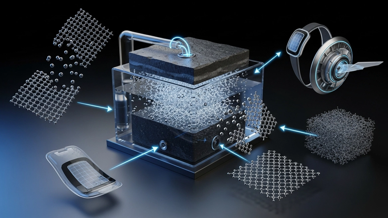
Section 6: Future Horizons & High-Value B2B Applications
The transformative potential of electrochemically exfoliated graphene (ECG) extends profoundly into next-generation energy storage and high-frequency electronic applications, driven by its tunable structural integrity and superior electrical characteristics. For advanced supercapacitors, ECG offers exceptional specific capacitance, often exceeding 200 F/g, coupled with unparalleled power densities and cycle stability over 100,000 cycles, attributable to its high specific surface area (up to 1800 m^2/g) and rapid ion transport kinetics within its mesoporous architecture. In lithium-ion and solid-state batteries, ECG-based anodes and conductive additives significantly enhance charge/discharge rates and volumetric energy density, mitigating issues like dendrite formation and improving overall cell longevity. For high-frequency electronics operating in the terahertz regime, the inherent high carrier mobility of ECG (often >10,000 cm^2/Vs) and its low intrinsic electrical resistivity are paramount. Post-exfoliation treatments, such as rapid thermal annealing employing focused 3000K thermal pulses for sub-millisecond durations, are critical for minimizing sheet resistance to values below 100 Ohm/sq at 90% transparency for transparent conductive films, while simultaneously healing lattice defects and optimizing grain boundaries, thereby ensuring robust performance in demanding RF and photonics applications.
Beyond energy and electronics, the exceptional properties of ECG position it as a critical enabler for advanced sensing, environmental remediation, and thermal management solutions. Its vast surface area and tunable electronic band structure facilitate the development of ultrasensitive chemical and biosensors, capable of detecting analytes at parts-per-billion concentrations for gases like NO2 or picomolar levels for specific biomarkers, exhibiting response times often in the milliseconds due to highly efficient surface adsorption and charge transfer mechanisms. In environmental applications, ECG's functionalizable surface allows for highly efficient adsorption and catalytic degradation of pollutants. Empirical data demonstrates that ECG can achieve up to 79% heavy metal adsorption efficiency for ions such as Pb(II) and Cd(II) from aqueous solutions, leveraging strong electrostatic interactions and chelation, making it a superior sorbent for water purification systems. Furthermore, its intrinsic thermal conductivity, which can approach 3000 W/mK for highly crystalline electrochemically derived flakes, renders ECG an indispensable material for thermal interface materials and heat spreaders in high-power density computing architectures, mitigating localized hot spots and extending component lifespan in server farms and advanced microprocessors where conventional cooling solutions are reaching their limits.
The integration of ECG into structural composites, EMI shielding, and future smart materials represents another high-value B2B frontier. With loadings as low as 0.5-1.0 wt%, ECG can confer significant enhancements to polymer matrices, increasing tensile strength by over 30% and fracture toughness by 50%, while simultaneously providing electrical conductivity for antistatic applications or structural health monitoring. The controlled surface functionalization achievable through electrochemical exfoliation allows for optimized interfacial bonding, crucial for maximizing load transfer and preventing aggregation within the composite. For electromagnetic interference (EMI) shielding, thin films or composites incorporating ECG offer broadband attenuation exceeding 60 dB across X-band frequencies (8-12 GHz), critical for protecting sensitive electronics in aerospace, defense, and telecommunications from disruptive electromagnetic radiation, all while maintaining lightweight profiles. Moreover, the inherent piezoresistive properties of ECG, with gauge factors exceeding 500, enable the development of highly sensitive strain sensors for flexible robotics and smart textiles. This capacity for multi-modal integration, from mechanical reinforcement to active sensing and actuation, underscores ECG's pivotal role in evolving material science towards truly adaptive and responsive systems, driven by scalable and cost-effective electrochemical production methods.
Evaluate Our Quality
Serious about B2B integration? Test our premium Pulsed Electrical Resistive Carbon Heating turbostratic graphene in your lab. 100g sample packs available now.