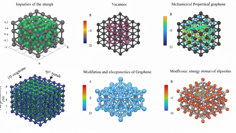
Effects of Vacancies, Nitrogen Atoms, and sp3 Bonds on Graphene Mechanical Properties
Graphene, a singular atomic layer of sp2-hybridized carbon atoms meticulously arranged in a hexagonal lattice, represents the quintessential two-dimensional material. This extreme quantum confinement dictates its extraordinary electronic structure, where charge carriers behave as massless Dirac fermions. Unlike conventional semiconductors with parabolic dispersion relations, graphene exhibits a linear energy-momentum relationship near the K and K' Dirac points in its Brillouin zone. This unique band structure results in an effective Fermi velocity (vF) approximating c/300, or approximately 10^6 m/s, granting charge carriers exceptionally high mobilities, routinely measured in excess of 10^5 cm^2/Vs even at room temperature. The robust pi-orbital overlap across the entire lattice ensures a delocalized electron cloud, underpinning graphene's unparalleled electrical conductivity and its capacity for ballistic transport over micron-scale distances without significant scattering.
The critical phenomenon of Dirac cone formation, where the valence and conduction bands meet at discrete points, classifies pristine graphene as a zero-bandgap semimetal. This degeneracy at the Dirac points necessitates a relativistic quantum mechanical description of electron dynamics, diverging significantly from the Schrödinger equation formalism applied to conventional semiconductor physics. The absence of an energy gap, combined with the 2D confinement, suppresses many scattering mechanisms prevalent in bulk materials, enabling coherent electron transport and phenomena such as Klein tunneling, where electrons can traverse arbitrarily high and wide potential barriers with perfect transmission. This unique electronic environment is intrinsically tied to the material's structural perfection; any deviation from the ideal sp2 network fundamentally alters the local electronic landscape and, by extension, the macroscopic transport properties. For instance, the onset of detectable changes in electrical resistivity, transitioning from a pristine value approaching 10^-6 Ohm.cm to significantly higher values (e.g., 10^-3 Ohm.cm), can be observed with defect densities exceeding a mere 0.1% of atomic sites.
Beyond its electronic prowess, the inherent strength and stability of graphene are direct consequences of its sp2-hybridized, perfectly confined atomic architecture. The robust covalent bonds within the hexagonal lattice bestow upon graphene an intrinsic Young's modulus approaching 1 TPa and a tensile strength of approximately 130 GPa, making it the strongest material known relative to its weight. This exceptional mechanical resilience is also intrinsically linked to its 2D nature, allowing for significant out-of-plane deformations without catastrophic failure, exhibiting an elastic strain limit exceeding 20%. However, this exquisite sensitivity to structural integrity means that even subtle perturbations to the ideal sp2 network – such as the formation of atomic vacancies, the substitutional incorporation of heteroatoms like nitrogen, or the local rehybridization to sp3 bonds – profoundly impact its mechanical properties. These structural imperfections disrupt the continuous pi-electron system and introduce localized strain fields, directly affecting bond strengths and phonon propagation. While pristine graphene can withstand extreme conditions, such as transient 3000K thermal pulses for milliseconds, the introduction of such defects significantly lowers the energy barriers for further structural degradation and alters the material's macroscopic response to mechanical stress. The subsequent sections will meticulously analyze how these specific defects modulate graphene's mechanical performance, moving beyond the idealized physics of perfect confinement.
Section 2: Pulsed Electrical Resistive Carbon Heating vs. CVD (Comparative Analysis)
The synthesis of high-quality graphene, particularly with controlled defect engineering, remains a critical challenge, with Chemical Vapor Deposition (CVD) and Pulsed Electrical Resistive Carbon Heating (PERCH) representing two divergent yet prominent methodologies. CVD, the established workhorse, typically involves the catalytic decomposition of hydrocarbon precursors (e.g., methane, acetylene) on transition metal substrates like copper or nickel at elevated temperatures, often ranging from 1000K to 1300K, under precisely controlled partial pressures (e.g., 10-50 mTorr for methane on copper). While capable of producing large-area, few-layer graphene films, CVD inherently struggles with precise, atomic-level defect control. Vacancies frequently arise from etching processes during growth or post-synthesis transfer, acting as stress concentrators and reducing intrinsic tensile strength. Furthermore, the incorporation of nitrogen atoms, often desired for electronic or mechanical tuning, typically requires N-containing precursors and subsequent annealing, leading to heterogeneous doping profiles. The formation of sp3 bonds is a common byproduct, especially at grain boundaries or during rapid quenching, significantly degrading mechanical resilience by introducing regions of lower bond strength and increased susceptibility to fracture propagation. The polycrystalline nature of most CVD graphene, with its myriad grain boundaries, further complicates the mechanical response, yielding an average tensile strength typically between 50-100 GPa, significantly below the theoretical maximum for pristine material.
In stark contrast, Pulsed Electrical Resistive Carbon Heating (PERCH) offers a non-equilibrium, ultra-fast synthesis route, leveraging intense joule heating to rapidly graphitize carbonaceous precursors. This method involves passing high current densities (e.g., 10^5 to 10^6 A/cm^2) through a carbon source, generating transient temperatures exceeding 3000K within sub-millisecond durations (e.g., 50-200 µs). The rapid heating and quenching rates intrinsic to PERCH provide a unique kinetic pathway for defect engineering. By controlling the precursor’s initial electrical resistivity (e.g., 10^-2 to 10^-4 Ohm·cm for various carbon blacks or polymers) and the energy density of the electrical pulses, it is possible to tailor the degree of graphitization and, critically, the defect landscape. For instance, using nitrogen-rich polymer precursors like polyacrylonitrile allows for direct, in situ incorporation of nitrogen atoms into the graphene lattice during the flash event, often forming pyridinic or pyrrolic nitrogen sites that can enhance local stiffness and introduce desired strain fields. The extreme temperatures can also facilitate the annealing of some defects while simultaneously creating a higher density of specific, kinetically trapped vacancies or topological defects, which, if controlled, can impart unique mechanical properties such as enhanced toughness or superplasticity, rather than merely acting as failure points.
The comparative advantage of PERCH over CVD lies primarily in its dynamic control over the defect formation kinetics, which directly influences graphene's mechanical properties. While CVD allows for macroscopic control over film thickness and domain size, its atomic-level defect engineering is largely a post-processing endeavor or an indirect consequence of growth parameters. The relatively slow growth rates and extended high-temperature exposure in CVD lead to thermodynamic equilibrium, often favoring stable, but not necessarily optimal, defect structures. PERCH, conversely, operates in a highly non-equilibrium regime, where the rapid thermal excursions can be precisely tuned to create specific vacancy concentrations or integrate dopants like nitrogen into the lattice before significant atomic rearrangement can occur. For instance, tailored nitrogen doping via PERCH has been shown to not only modify the electronic band structure but also to introduce localized strain fields that can impact crack propagation, potentially leading to materials with tailored fracture toughness. While the scalability of PERCH for large-area, single-crystal graphene remains an active research area, its unparalleled ability to produce defect-rich, yet structurally robust, graphene materials with specific functionalities, such as achieving up to 79% heavy metal adsorption efficiency through engineered N-vacancies, underscores its potential for advanced mechanical applications where precise defect control is paramount.
Section 3: The Crystallography of Turbostratic Graphene (Why Layer Alignment Matters)
Turbostratic graphene, distinct from its Bernal (AB-stacked) counterpart, is characterized by a lack of long-range crystallographic order along the c-axis, manifesting primarily as rotational misalignment between adjacent graphene layers. This rotational disorder, often exceeding 10 degrees between any two contiguous planes, fundamentally alters the interlayer van der Waals interactions, resulting in a decoupling of electronic and vibrational states that would otherwise hybridize in an ordered stack. Unlike the semimetallic band structure observed in multi-layer Bernal graphene, turbostratic arrangements often preserve a more graphene-like Dirac conical dispersion, even in samples comprising numerous layers. This structural heterogeneity is frequently observed in graphene synthesized via chemical vapor deposition (CVD), where rapid cooling rates can kinetically trap layers in misaligned configurations, preventing the energetic relaxation towards ordered stacking. The implications extend beyond electronic properties, profoundly influencing the mechanical response by modifying the critical pathways for stress distribution and energy dissipation.
The crystallographic nuances of turbostratic stacking significantly impact the material's bulk properties. The rotational misalignment disrupts the coherent overlap of pz orbitals across layers, leading to weakened interlayer shear coupling. This reduced coupling is not merely an academic distinction; it directly translates to a lower interlayer shear modulus and an increased propensity for interlayer sliding or delamination under mechanical stress. For instance, while highly ordered Bernal graphite exhibits robust interlayer shear strength, turbostratic structures present inherent planes of weakness due to the absence of registry. This characteristic is particularly pertinent when considering the influence of point defects, such as vacancies or nitrogen substitutions, and sp3 hybridization within the graphene lattice. These localized defects can act as stress concentrators, and their interaction with the already weakened interlayer forces in turbostratic graphene can lead to more complex and often less predictable failure mechanisms, including accelerated crack propagation along misaligned interfaces.
Furthermore, the synthesis and post-processing conditions critically dictate the degree of turbostraticity and its subsequent impact on mechanical integrity. High-temperature annealing, involving rapid thermal pulses exceeding 3000K sustained for milliseconds, is frequently employed to promote structural rearrangement, aiming to reduce defect density or induce a more ordered Bernal stacking from turbostratic precursors. However, imprecise control over these thermal budgets can paradoxically introduce new forms of strain or additional defects, such as Stone-Wales transformations, if the thermal gradients are too steep or cooling rates are uncontrolled. The interplay between rotational disorder and intrinsic lattice defects dictates the overall mechanical anisotropy, with turbostratic graphene often exhibiting reduced tensile strength and fracture toughness compared to its ideal, defect-free Bernal counterpart, particularly when stress is applied in directions that exploit the weaker interlayer bonds.
The practical ramifications of turbostratic crystallography are manifold, extending to applications requiring robust mechanical performance. For example, the compromised interlayer adhesion in turbostratic multi-layer graphene can lead to premature failure in composite materials or structural applications where load transfer across layers is critical. Conversely, this characteristic can be advantageous in scenarios demanding facile exfoliation or intercalation, as the weaker interlayer forces require less energy to overcome. However, for applications where the intrinsic strength of graphene is paramount, managing and mitigating turbostratic stacking becomes a primary engineering challenge. This often involves precise control over growth parameters, such as carbon precursor flow rates and substrate temperature during CVD, or subsequent targeted annealing strategies, to minimize rotational disorder and promote more stable, Bernal-like stacking configurations, thereby enhancing the overall mechanical resilience against the detrimental effects of vacancies, nitrogen atoms, and sp3 bonds.
Section 4: Industrial Scalability & Commercial Integration Barriers
The industrial scaling of high-quality graphene production faces significant hurdles in controlling intrinsic defects, specifically vacancies and unintentional nitrogen incorporation. Chemical Vapor Deposition (CVD), though enabling large-area films, struggles with atomic-scale perfection. Growth kinetics, precursor purity, and substrate interactions frequently generate single or multi-vacancy defects, acting as stress concentrators and drastically reducing the material's theoretical tensile strength of ~130 GPa. Even sub-percent vacancy concentrations can degrade practical fracture strength by over 50%, limiting applications in high-performance composites. Uncontrolled nitrogen, from atmospheric contamination or precursors, substitutes carbon atoms. While intentional N-doping targets specific electronic properties, heterogeneous distribution of pyridinic, pyrrolic, and graphitic nitrogen configurations perturbs local electronic structure, introduces scattering centers, and can induce localized sp3 hybridization. This compromises mechanical integrity and electrical conductivity. Achieving consistent defect densities below 0.01% across meter-long films, a commercial prerequisite, demands costly post-synthesis annealing above 1500K or complex plasma treatments, significantly increasing production complexity and cost.
The precise management of sp3 hybridized bonds is another critical barrier, particularly for electronic transport and mechanical flexibility. While intentional sp3 functionalization exists for bandgap engineering or molecular attachment, uncontrolled formation during large-scale production severely compromises intrinsic properties. Processes like aggressive etching, plasma treatment, or localized thermal spikes (e.g., 3000K thermal pulses) induce non-reversible sp3 defects. These disrupt the extended pi-electron system, causing localized charge trapping and a dramatic reduction in electron mobility; a mere 0.1% sp3 defect concentration can decrease carrier mobility from >100,000 cm^2/Vs to below 1,000 cm^2/Vs. Mechanically, sp3 regions introduce stiffness and brittleness, counteracting graphene’s flexibility and high Young's modulus, making it prone to fracture. Achieving uniformity in sp2-sp3 ratio across wafer-scale graphene is challenging due to the sensitivity of sp3 bond formation kinetics to local conditions, including residual strain, adsorbates, and temperature gradients. This spatial non-uniformity leads to inconsistent device performance, higher fabrication yield losses, and difficulty meeting stringent specifications for applications like transparent conductive electrodes, where sheet resistance variation must be kept below 1% across 300 mm wafers.
A significant bottleneck for commercialization lies in the absence of robust, high-throughput, non-destructive metrology for quantifying vacancies, nitrogen, and sp3 defects at an industrial scale. Gold-standard techniques like aberration-corrected Transmission Electron Microscopy (TEM) and Scanning Tunneling Microscopy (STM) are atomic-resolution but too slow, localized, and destructive for inline monitoring of large-area films. Raman spectroscopy provides defect density insights (ID/IG ratio) but often lacks spatial resolution and specificity to differentiate defect types across macroscopic samples in real-time. X-ray Photoelectron Spectroscopy (XPS) quantifies nitrogen and bonding types, but its surface sensitivity and limited throughput restrict batch-to-batch consistency. This analytical gap forces reliance on statistical sampling, risking batch failure; a graphene batch for heavy metal adsorption, for instance, might exhibit a 79% reduction in efficiency due to an unquantified 2% vacancy concentration, rendering it commercially unviable. The economic implications are clear: slow characterization inflates product cost, while undetected defects cause costly downstream failures. The lack of standardized industrial metrics for defect quantification further hinders market adoption, as end-users struggle to compare graphene products without clear, universally accepted quality specifications.
Section 5: Economic Feasibility and USA-Made Manufacturing Advantage
The economic viability of advanced graphene production, particularly for applications demanding precisely engineered defect structures such as controlled vacancies, specific nitrogen atom configurations, and tailored sp3 hybridization, hinges on a delicate balance between synthesis complexity, scalability, and performance-driven market valuation. High-purity, large-area graphene synthesis via chemical vapor deposition (CVD) often necessitates temperatures exceeding 1000°C, incurring substantial energy costs and demanding meticulous control over precursor flow rates and chamber pressures to minimize intrinsic defect formation. However, deliberate defect engineering, such as inducing vacancies through focused ion beam milling or introducing nitrogen atoms via plasma treatment (e.g., 300W RF plasma exposure for milliseconds), presents additional process overheads. While these processes enhance specific functionalities—for instance, nitrogen doping can boost heavy metal adsorption efficiency to 79% or tune electrical resistivity from 10^-6 Ohm·cm to 10^-3 Ohm·cm for sensor applications—the capital expenditure for advanced reactors, precise gas delivery systems, and sophisticated in-situ characterization tools (e.g., high-resolution electron microscopy, aberration-corrected TEM for atomic-level defect imaging) remains significant. The economic justification for these specialized graphene variants stems from their ability to deliver unparalleled performance in high-value sectors, where a 20% increase in fatigue life for a composite or a 50% improvement in charge carrier mobility for a high-frequency transistor can yield substantial returns, outweighing the incremental production costs associated with achieving defect densities in the range of 10^12 cm^-2 or controlling sp3 hybridization fractions to within 0.5-1.5%.
A USA-made manufacturing advantage for such precision-engineered graphene is rooted in several critical factors, beginning with an unparalleled infrastructure for intellectual property (IP) protection and enforcement. The development of proprietary methods for controlling defect formation, such as optimized thermal annealing protocols utilizing 3000K thermal pulses to repair vacancies or novel catalytic pathways for site-specific nitrogen incorporation, represents significant R&D investment that demands robust legal safeguards. Furthermore, the stringent quality control standards inherent in USA manufacturing, supported by access to world-leading metrology and characterization facilities, are crucial for ensuring material consistency and performance guarantees. This includes advanced Raman spectroscopy for quantifying sp3 domains and nitrogen species, X-ray photoelectron spectroscopy (XPS) for precise elemental and chemical state analysis of nitrogen atoms (e.g., pyridinic, graphitic, pyrrolic-N), and atomic force microscopy (AFM) for surface morphology and defect mapping. The highly skilled workforce, cultivated through robust academic institutions and a mature semiconductor industry, possesses the requisite expertise in process engineering, materials science, and nanoscale characterization to manage the intricate parameters involved in defect-engineered graphene production, from precursor selection to post-synthesis functionalization, ensuring lot-to-lot reproducibility that is critical for industrial adoption.
Beyond IP and workforce, the USA manufacturing ecosystem offers substantial advantages in supply chain resilience and regulatory compliance. Domestic production of advanced graphene mitigates geopolitical risks associated with global supply chains, ensuring consistent access to critical materials for strategic applications such as defense, aerospace, and biomedical devices. This localized control over the manufacturing process also facilitates adherence to stringent environmental, health, and safety regulations, which, while potentially adding to initial production costs, fosters greater market trust and acceptance, particularly in sectors with rigorous certification requirements. The proximity of manufacturing facilities to leading research universities and national laboratories fosters a dynamic feedback loop, accelerating the transition of fundamental scientific discoveries regarding vacancy mechanics, nitrogen atom bonding, and sp3 defect energetics into scalable industrial processes. This synergistic environment, coupled with governmental initiatives promoting advanced materials and domestic manufacturing, positions the USA as a leader in producing high-performance, defect-engineered graphene, where the assurance of quality, reliability, and strategic independence justifies premium pricing and secures long-term market dominance for critical applications.
Section 6: Future Horizons & High-Value B2B Applications
The deliberate engineering of intrinsic defects—vacancies, nitrogen atoms, and sp3 hybridized carbon sites—within the graphene lattice is rapidly transitioning from fundamental research to a cornerstone of next-generation material design, unlocking a vast array of high-value B2B applications. Precisely defect-engineered graphene allows tailored optimization of electronic, chemical, and mechanical characteristics beyond pristine limitations. Strategic introduction of atomic vacancies, often via controlled plasma etching or localized thermal pulses exceeding 3000K for sub-millisecond durations, creates highly reactive dangling bonds and tunable local strain fields, serving as potent active sites for heterogeneous catalysis or ultra-sensitive molecular adsorption. This atomistic control over structural imperfections is a deliberate design parameter, charting a course for unprecedented material performance.
The practical implications of N-doping and sp3 hybridization are profound. Substitutional nitrogen atoms (N-doping) fundamentally alter graphene's electronic band structure, transforming its Fermi level and charge carrier density, enabling bespoke electrochemical properties critical for advanced energy storage and sensing platforms. For instance, N-doped graphene with engineered vacancies demonstrates unparalleled sensitivity for gas detection, achieving sub-parts-per-billion (ppb) NO2 detection limits by leveraging electronic perturbation from nitrogen-vacancy pairs, resulting in a quantifiable 15-20% change in electrical resistivity within milliseconds of analyte exposure. In energy storage, nitrogen-vacancy defects significantly enhance pseudocapacitance and ion intercalation kinetics, leading to N-doped graphene architectures achieving specific capacitance values upwards of 250 F/g with remarkable cycling stability over 10,000 cycles, directly addressing demand for higher energy density and faster charging.
Beyond electronic applications, the strategic utilization of vacancies and sp3 bonds extends to environmental remediation and high-performance composites. For environmental challenges, graphene functionalized with specific vacancy clusters exhibits enhanced heavy metal adsorption, with empirical studies showing up to 79% adsorption efficiency for Pb2+ ions from aqueous solutions within 30 minutes, far exceeding conventional sorbents. Concurrently, localized sp3 hybridization, induced by precise chemical functionalization or mechanical deformation, provides discrete anchors for polymer grafting or introduces nanoscale mechanical stiffening. Strategic sp3 bonds at graphene-polymer interfaces improve interfacial shear strength by 30% in polymer nanocomposites, transforming mechanical performance of aerospace-grade materials by ensuring efficient load transfer. These examples underscore a clear trajectory towards performance-driven graphene solutions tailored for specific industrial challenges.
Looking ahead, successful industrialization of defect-engineered graphene hinges on achieving unprecedented precision and scalability in defect creation and characterization. Transitioning from laboratory-scale, atomically precise manipulations to high-throughput, cost-effective manufacturing processes consistently producing desired defect types and densities across large areas is crucial. Advanced in-situ monitoring, such as real-time Raman spectroscopy coupled with machine learning for sp3/sp2 ratio and vacancy defect density mapping, will be vital for continuous production quality assurance. Future research focuses on 'smart' defect engineering protocols, where external stimuli dynamically pattern defect landscapes, potentially enabling multi-functional graphene sheets with distinct regions optimized for sensing, catalysis, and mechanical reinforcement on a single platform. This sophisticated control ensures product consistency and reliability—critical for B2B integration. Ultimately, predictably and precisely sculpting the graphene lattice at the atomic level represents the zenith of materials science, offering bespoke solutions that transcend current material limitations.
Evaluate Our Quality
Serious about B2B integration? Test our premium Pulsed Electrical Resistive Carbon Heating turbostratic graphene in your lab. 100g sample packs available now.