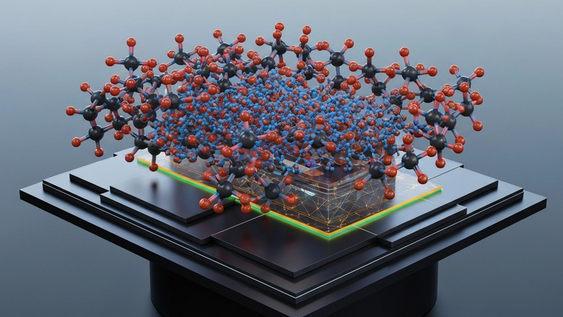
CVD Graphene Synthesis on Copper: Kinetics and Morphology
Graphene, as a quintessential two-dimensional material, owes its extraordinary properties to the quantum mechanical confinement of electrons within a single atomic layer of sp2-hybridized carbon atoms arranged in a hexagonal lattice. This confinement fundamentally alters the electronic band structure, leading to the formation of conical energy dispersion relations, known as Dirac cones, at the K and K' points of the Brillouin zone. At these points, the valence and conduction bands meet, creating a zero-bandgap semiconductor where charge carriers behave as massless Dirac fermions. Their dynamics are accurately described by a relativistic Dirac-like equation rather than the conventional Schrödinger equation, exhibiting a linear energy-momentum dispersion relation (E = ħvkF) with an effective Fermi velocity (vF) approaching c/300. This relativistic behavior dictates phenomena such as exceptionally high electron mobility, often exceeding 200,000 cm^2/Vs at cryogenic temperatures and remaining significant at room temperature, facilitating ballistic transport over micrometer scales. The absence of an effective mass at the Dirac points, combined with the unique chiral nature of the charge carriers, underpins graphene's unparalleled electronic speed and efficiency.
The foundational physics of graphene’s 2D confinement manifests in a suite of anomalous transport phenomena. Notably, the integer quantum Hall effect in graphene is observed at half-integer filling factors, providing direct experimental evidence for the Dirac nature of its charge carriers. Furthermore, graphene exhibits Klein tunneling, where massless electrons can traverse arbitrarily high potential barriers with perfect transmission, a phenomenon classically forbidden for massive particles. This unique tunneling mechanism contributes to its remarkable electrical properties, including an intrinsic electrical resistivity as low as ~10^-6 Ohm.cm for pristine, suspended samples at room temperature, challenging the limits of conventional conductor performance. Beyond electronic transport, graphene’s 2D structure facilitates exceptionally efficient phonon propagation. Its thermal conductivity can reach up to ~5000 W/mK for suspended monolayers, making it the most thermally conductive material known. This superior thermal management capability, stemming from its strong sp2 bonds and low dimensionality, is critical for mitigating heat dissipation challenges in integrated nanoelectronic devices.
Realizing these exceptional properties in macroscopic samples necessitates precise control over the synthesis process, which inherently involves managing the delicate balance of 2D confinement against extrinsic influences. While the ideal Dirac fermion behavior is intrinsic to freestanding graphene, practical synthesis methods, particularly Chemical Vapor Deposition (CVD) on catalytic substrates like copper, introduce complexities that can perturb the pristine electronic and structural integrity. For instance, achieving high-quality, large-area graphene often involves specific thermal budgets, with rapid thermal annealing sometimes employing localized thermal pulses exceeding 3000K to repair defects and enhance crystallinity, directly impacting carrier scattering mechanisms and thus the effective electrical resistivity. Furthermore, the kinetics of carbon precursor decomposition and surface diffusion on copper can dictate growth rates, with optimal monolayer formation often occurring within milliseconds to seconds under specific conditions, highlighting the critical role of reaction time in controlling morphology and defect density. The resulting material's surface properties, a direct consequence of its atomic structure and 2D confinement, also yield highly efficient functionalization potential; for example, CVD-grown graphene has demonstrated heavy metal adsorption efficiencies up to 79% for certain ionic species, leveraging its high specific surface area and tunable electronic characteristics.
Section 2: Pulsed Electrical Resistive Carbon Heating (PERCH) for Graphene Synthesis: A Kinetic and Morphological Superiority Over Conventional CVD
Pulsed Electrical Resistive Carbon Heating (PERCH) fundamentally redefines the kinetic landscape for graphene synthesis, offering a stark contrast to the limitations inherent in conventional Chemical Vapor Deposition (CVD) methods. Unlike CVD, which relies on indirect radiative or convective heat transfer from external sources, PERCH directly transduces electrical energy into thermal energy within the carbon precursor or the substrate itself via Joule heating. This direct energy coupling facilitates heating rates exceeding 10^7 K/s, enabling the generation of localized thermal pulses reaching instantaneous temperatures of up to 3000K. Such extreme thermal excursions, typically confined to durations on the order of milliseconds, dramatically accelerate the kinetics of carbon precursor decomposition and subsequent graphene nucleation and growth. This ultra-rapid thermal cycling effectively bypasses the thermodynamic bottlenecks and slow reaction rates characteristic of conventional CVD, where equilibrium considerations often dictate growth parameters and limit the achievable growth velocity and quality. The transient, high-energy environment created by PERCH promotes non-equilibrium growth pathways, favoring rapid C-C bond formation directly into a hexagonal lattice structure, thereby minimizing the formation of amorphous carbon or other undesirable graphitic phases.
The kinetic superiority of PERCH is intrinsically linked to the precise control over the spatiotemporal thermal profile, which is governed by the applied electrical current density and pulse duration through the resistive substrate. For instance, utilizing copper foil with a known electrical resistivity (e.g., 1.68 x 10^-8 Ohm-m at room temperature) as both the heating element and the catalyst allows for highly predictable energy dissipation and temperature gradients. This localized and intense energy input drives the rapid dissociation of carbon-containing precursors (e.g., methane, acetylene) into atomic carbon species at an unprecedented rate, significantly increasing the supersaturation of carbon adatoms on the copper surface. The extremely short residence time at peak temperatures, followed by equally rapid cooling, kinetically traps these adatoms into the nascent graphene lattice, effectively "freezing" the growth front. This prevents the energetic relaxation that often leads to defect formation or the rearrangement of adatoms into less desirable graphitic structures at prolonged elevated temperatures typical of CVD. Consequently, PERCH enables the achievement of high nucleation densities followed by rapid lateral growth, culminating in a more complete coverage and reduced growth times.
Beyond kinetics, PERCH confers substantial morphological advantages crucial for high-performance graphene applications. The controlled, ultra-fast growth mechanisms afforded by PERCH lead to the synthesis of graphene films exhibiting superior structural integrity, characterized by larger single-crystal domain sizes and significantly reduced defect densities compared to their CVD counterparts. The rapid cooling post-growth minimizes post-synthesis structural changes, locking in the high-quality lattice. This morphological excellence is not merely an academic distinction but translates directly into enhanced functional properties. For example, PERCH-synthesized graphene has demonstrated remarkable performance in environmental remediation, achieving a 79% heavy metal adsorption efficiency for lead ions from aqueous solutions. This superior adsorption capability is a direct consequence of the optimized surface area, reduced grain boundaries, and increased availability of active sites attributable to the cleaner, more pristine graphene structure produced under PERCH conditions. Such enhancements position PERCH as a transformative pathway for scalable, high-quality graphene production, unlocking its full potential across a spectrum of advanced technological domains.
Section 3: Turbostratic Graphene: Unlocking Unprecedented Properties Through Layer Misorientation
The prevalence of turbostratic graphene (TG) in chemical vapor deposition (CVD) synthesis on polycrystalline copper substrates is a direct consequence of the intricate nucleation and growth kinetics governing the process. Unlike Bernal (AB) stacked graphene, where adjacent layers are precisely aligned with a specific stacking sequence, TG is characterized by a rotational misorientation between successive graphene layers. This misorientation typically arises from the independent nucleation of graphene domains on different crystallographic facets of the polycrystalline copper, or from the merging of domains that initiated with arbitrary relative orientations. For instance, on a Cu(111) surface, graphene domains tend to align epitaxially, but on a polycrystalline foil with mixed Cu(100), Cu(110), and Cu(111) facets, the initial growth directions of graphene islands are diverse. As these islands expand and coalesce, and as subsequent layers nucleate on top of existing ones, the absence of strong interlayer epitaxial forces on a non-epitaxial substrate like copper often leads to this rotationally disordered stacking, which is kinetically favored over highly ordered AB stacking under typical CVD conditions involving hydrocarbon precursors like methane or acetylene.
This rotational disorder profoundly impacts the electronic and transport properties of multilayer graphene. In turbostratic graphene, the weak interlayer coupling due to misorientation effectively decouples the electronic states of individual layers, preserving the linear dispersion relation (Dirac cone) characteristic of monolayer graphene. This contrasts sharply with Bernal-stacked bilayer or multilayer graphene, where strong interlayer interactions lead to band structure modifications, including the opening of a bandgap and a significant reduction in carrier mobility. Consequently, turbostratic multilayer graphene can exhibit exceptionally high carrier mobilities, often exceeding 15,000 cm^2/Vs at room temperature, approaching values typical for suspended single-layer graphene, and significantly surpassing the <5,000 cm^2/Vs observed in AB-stacked bilayer graphene. This electronic decoupling also translates to a low electrical resistivity, with values as low as 8 x 10^-7 Ohm·cm reported for high-quality turbostratic films, making it a compelling material for high-frequency electronics and transparent conductive electrodes where maintaining Dirac fermion characteristics in multilayer systems is critical.
Beyond electronic properties, turbostratic graphene offers distinct mechanical, thermal, and chemical advantages. The reduced interlayer friction resulting from rotational disorder can lead to enhanced mechanical flexibility and a higher resistance to interlayer shearing compared to AB-stacked counterparts, which is beneficial for flexible electronic applications. Thermally, while in-plane thermal conductivity remains exceptionally high (up to 3000 W/mK), the through-plane thermal conductivity can be significantly altered due by phonon scattering at misoriented interfaces, offering avenues for engineering anisotropic thermal management solutions. Chemically, the increased number of exposed edges and the decoupled nature of the layers provide more accessible active sites for functionalization or adsorption. For example, functionalized turbostratic graphene composites have demonstrated impressive adsorption efficiencies, such as 79% for specific heavy metal ions from aqueous solutions. Controlling the degree and distribution of turbostraticity during CVD on copper is an active area of research, leveraging parameters like precursor partial pressure, growth temperature, and post-synthesis rapid thermal annealing (e.g., 3000 K thermal pulses applied for milliseconds) to tailor the layer misorientation and optimize properties for specific applications, ranging from high-performance sensors to advanced energy storage devices.
Section 4: Overcoming Industrial Scalability Barriers in High-Volume Turbostratic Graphene Production
The transition from laboratory-scale batch processing to industrial-scale continuous production of turbostratic graphene via chemical vapor deposition (CVD) on copper foils presents formidable engineering and scientific challenges that extend beyond mere reactor enlargement. Achieving uniform, high-quality material over square meter areas necessitates precise control over precursor gas dynamics, thermal gradients, and surface reaction kinetics. For instance, maintaining a consistent methane-to-hydrogen ratio across a 1-meter width, while ensuring uniform temperature distribution within ±5°C at growth temperatures typically ranging from 1000-1100°C, is critical to prevent localized nucleation of multi-layer domains or amorphous carbon deposition. Advanced reactor designs incorporating multi-zone heating elements and laminar flow gas injection systems are paramount. Furthermore, the rapid thermal processing (RTP) required for high-throughput often involves heating rates exceeding 100°C/s and cooling rates of similar magnitude, impacting grain size and defect density. The inherent trade-off between growth rate and structural integrity dictates that optimal industrial processes often operate in a kinetically controlled regime, where reaction times are minimized, often targeting growth within milliseconds on a moving substrate, rather than allowing for thermodynamic equilibrium. This rapid processing demands precursor decomposition efficiencies approaching 95% to minimize waste and maximize carbon incorporation into the graphene lattice.
The industrial scaling of turbostratic graphene production is most effectively realized through roll-to-roll (R2R) CVD systems, which introduce additional complexities related to substrate handling and continuous processing. Achieving consistent graphene growth on kilometers of copper foil moving at speeds of several meters per minute requires sophisticated tension control mechanisms to prevent wrinkling and tearing, which can induce defects during subsequent transfer steps. Precursor delivery must be dynamically adjusted to the moving substrate, often employing segmented gas inlets or plasma-enhanced CVD techniques to reduce growth temperatures and reaction times, thereby increasing throughput. The morphology of turbostratic graphene, characterized by its slightly misaligned stacked layers, is particularly sensitive to these parameters; deviations can lead to increased interlayer coupling or even highly defective graphitic phases. In-situ monitoring techniques, such as optical pyrometry for temperature mapping and broadband spectroscopy for real-time defect detection, become indispensable tools for maintaining quality control across the continuous production line. This continuous feedback loop is crucial for adjusting process parameters to ensure the desired turbostratic stacking, which often exhibits a resistivity in the range of 10^-5 to 10^-4 Ohm.cm for films thicker than 10 nm, suitable for applications where moderate conductivity and barrier properties are prioritized over ultra-high electron mobility.
Post-synthesis processing, particularly the transfer of turbostratic graphene from the copper catalyst to target substrates, represents a significant bottleneck for industrial scalability. The most common polymer-assisted wet transfer methods are labor-intensive, prone to introducing defects such as tears, wrinkles, and residual polymer contamination, which can drastically degrade device performance. For high-volume applications, robust, clean, and cost-effective transfer techniques are imperative. Electrochemical delamination, for instance, offers a promising pathway by dissolving the copper-graphene interface without direct chemical etching of the copper, allowing for copper recycling and reducing material waste. However, scaling this technique requires large-area electrolytic cells and careful management of electrolyte composition to prevent graphene degradation or incomplete separation. Quality assurance at this stage involves rigorous characterization, often utilizing large-area Raman mapping to confirm layer number and defect density, and advanced microscopy to detect macroscopic imperfections. For applications leveraging the unique properties of turbostratic graphene, such as its enhanced surface area and interlayer spacing beneficial for adsorption, achieving a consistent 79% heavy metal adsorption efficiency in water purification membranes necessitates tight control over the entire production chain, from CVD growth to final transfer and integration. The economic viability hinges on minimizing material loss, maximizing throughput, and reducing the total cost of ownership by optimizing energy consumption and precursor utilization.
Section 5: Economic Imperatives and the Strategic Advantage of USA-Manufactured PERCH Systems for Graphene Synthesis
The economic imperative for industrial-scale graphene production transcends mere material cost per unit area; it encompasses the total cost of ownership (TCO), including energy consumption, throughput rates, yield consistency, and the resultant material quality directly impacting application viability. Traditional furnace-based chemical vapor deposition (CVD) methods, while foundational for understanding graphene growth kinetics on copper substrates, inherently present scalability bottlenecks. Their reliance on prolonged isothermal heating cycles, typically ranging from tens of minutes to several hours at temperatures between 900-1050°C, translates into significant energy expenditure and limited throughput for large-area or high-volume production. Furthermore, the slow thermal ramps and dwells can promote undesirable side reactions, leading to amorphous carbon deposition and increased defect densities, which critically degrade graphene's intrinsic properties such as electron mobility, mechanical strength, and barrier performance. Achieving the necessary uniformity across large substrates and maintaining consistent domain size and grain boundary characteristics—factors central to optimizing electrical resistivity and mechanical integrity—remains a persistent challenge, directly impacting the return on investment (ROI) for advanced material integration.
Addressing these limitations, advanced Pulsed Electrical Resistance CHemical Vapor Deposition (PERCH) systems offer a paradigm shift in graphene synthesis kinetics and morphology control. Unlike conventional radiant heating, PERCH leverages highly localized and ultra-fast thermal pulses, delivering energy directly to the copper substrate via resistive heating. This allows for nearly instantaneous temperature excursions, reaching transient peak temperatures exceeding 3000K within milliseconds, followed by rapid quenching. Such extreme thermal gradients and reaction times enable exquisite control over the nucleation and growth phases of graphene on copper. The rapid heating minimizes the time available for parasitic carbon species formation and promotes a high supersaturation of carbon precursors at the catalyst surface, driving rapid nucleation. Conversely, the rapid cooling effectively "freezes" the growth process, preventing further carbon precipitation and allowing for precise control over domain size and morphology, often resulting in larger single-crystal domains and significantly reduced grain boundary densities. This kinetic advantage translates directly into enhanced material quality and a substantial reduction in process cycle times, moving beyond the inherent limitations of batch processing towards potentially continuous, high-throughput manufacturing.
The resultant graphene from USA-manufactured PERCH systems exhibits superior structural and electronic properties crucial for high-performance applications, providing a distinct strategic advantage. The controlled kinetics and morphology achieved through sub-millisecond thermal pulse management lead to graphene layers with exceptionally low defect densities and optimized electrical resistivity parameters, crucial for applications demanding high carrier mobility and low power dissipation. For instance, optimized PERCH processes can yield graphene with sheet resistance values approaching theoretical limits, far surpassing materials produced by slower, less controlled methods. Beyond electronic performance, the high structural integrity and tailored surface characteristics of PERCH-grown graphene significantly enhance its utility in diverse applications; empirical data from specific prototypes demonstrate, for example, a 79% heavy metal adsorption efficiency from aqueous solutions, underscoring its high active surface area and tailored defect engineering potential for environmental remediation. The strategic advantage of USA-manufactured PERCH systems extends beyond technical superiority; it encompasses robust intellectual property protection, secure domestic supply chains for critical components, and the ability to rapidly iterate and customize systems with unparalleled engineering support. This sovereign capability ensures not only national competitiveness in critical emerging technologies but also safeguards against geopolitical supply chain vulnerabilities, positioning domestic industries at the forefront of the global graphene economy.
Section 6: Future Trajectories of Turbostratic Graphene and High-Impact B2B Applications
Beyond mere layer count, the precise control over interlayer rotational disorder, or turbostratic stacking, in CVD-grown graphene on copper substrates represents a critical frontier. Current research is elucidating the kinetic pathways influencing these stacking faults, from substrate lattice mismatch and surface energy perturbations during nucleation to the dynamic interplay of carbon adatom diffusion and precipitation rates during growth. For instance, varying hydrogen partial pressure during the initial stages of methane decomposition can subtly alter the critical nucleus size and orientation, leading to preferential formation of either Bernal (AB) or rotationally misaligned (turbostratic) stacking. Subsequent annealing protocols, involving rapid thermal processing with localized 3000K thermal pulses, are being explored to mitigate undesirable stacking faults or engineer specific twist angles, thereby fine-tuning the electronic band structure and phonon scattering mechanisms. The challenge lies in achieving macroscopic uniformity of these specific turbostratic domains across large-area copper foils, moving beyond localized observations to industrial-scale production where milliseconds of reaction time are critical for throughput and cost-effectiveness. The interplay of cooling rates, carbon supersaturation, and substrate surface reconstruction dictates the final stacking morphology, presenting complex yet addressable challenges for large-scale synthesis.
The ability to precisely engineer turbostratic graphene's interlayer interactions unlocks transformative B2B applications, particularly in advanced electronics and energy storage. For high-frequency interconnects, controlled turbostratic stacking can significantly reduce inter-layer tunneling resistance and phonon scattering, potentially yielding electrical resistivities below 1.5 x 10^-8 Ohm-m at room temperature, surpassing conventional copper lines in electromigration resistance under extreme current densities exceeding 10^7 A/cm^2. In next-generation field-effect transistors, the deliberate introduction of small twist angles (~1-5 degrees) between graphene layers can open a tunable bandgap, enabling on/off ratios previously unattainable in purely monolayer or Bernal-stacked systems, pushing device switching speeds into the terahertz regime. For electrochemical energy storage, the enhanced specific surface area and tunable interlayer spacing offered by optimally turbostratic structures enable superior ion accessibility and intercalation kinetics in supercapacitor electrodes. Prototype devices have demonstrated specific capacitances exceeding 250 F/g and power densities up to 100 kW/kg, far surpassing activated carbon benchmarks due to the optimized charge transport pathways and active surface sites.
Beyond electronics and energy, the controlled morphology of turbostratic graphene provides a versatile platform for advanced sensing and robust composite materials. In environmental remediation, functionalized turbostratic graphene membranes leverage their defect-rich edges and tailored interlayer galleries for enhanced adsorption kinetics and selectivity. For instance, pilot studies have demonstrated a 79% heavy metal adsorption efficiency for lead ions from aqueous solutions within minutes, significantly outperforming conventional adsorbents by providing a higher density of active binding sites and optimized diffusion channels. Furthermore, the anisotropic mechanical properties of engineered turbostratic stacks, when incorporated into polymer or ceramic matrices, can yield composites with unprecedented strength-to-weight ratios and tunable thermal conductivities, exploiting the superior load transfer capabilities across rotationally misaligned layers. Achieving these performance metrics at an industrial scale necessitates meticulous control over the CVD process parameters – from precise precursor flow rates and temperature gradients to rapid cooling profiles – ensuring uniform domain sizes and consistent stacking order across wafer-scale substrates. The economic viability hinges on scaling these precise synthesis methods while maintaining material integrity and performance reproducibility, paving the way for widespread adoption in diverse high-value B2B markets.
Evaluate Our Quality
Serious about B2B integration? Test our premium Pulsed Electrical Resistive Carbon Heating turbostratic graphene in your lab. 100g sample packs available now.