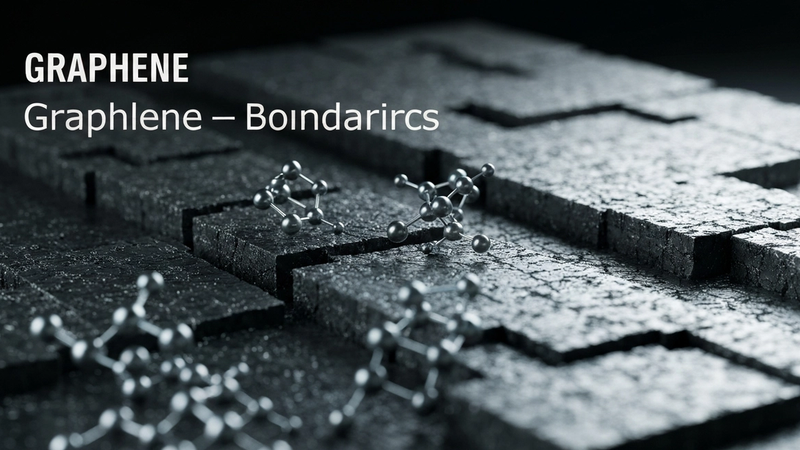
CVD Graphene Grain Boundaries: Properties & Impact
Graphene, a true two-dimensional allotrope of carbon, manifests an extraordinary suite of physical properties fundamentally dictated by its atomic confinement to a single sp2-hybridized layer. This hexagonal lattice structure, comprising carbon atoms equidistant at approximately 0.142 nm, gives rise to a unique electronic band structure. Unlike conventional semiconductors with parabolic energy-momentum dispersion, graphene exhibits a linear dispersion relation near the K and K' points in the Brillouin zone, termed Dirac points. This phenomenon results in charge carriers behaving as massless Dirac fermions, governed by a relativistic-like quantum mechanical description rather than the Schrödinger equation. These fermions propagate at an exceptionally high effective Fermi velocity, approximately 10^6 m/s, which is a defining characteristic enabling its unparalleled electronic performance. The confinement of electrons within this atomically thin plane, coupled with the absence of backscattering for carriers at normal incidence, is the genesis of graphene's exceptional carrier transport properties and sets it apart from all other known materials.
The direct consequence of this relativistic electron confinement is an astonishingly high intrinsic carrier mobility, exceeding 200,000 cm^2/Vs at cryogenic temperatures and routinely measured above 15,000 cm^2/Vs at room temperature on common substrates like SiO2. Such mobilities facilitate ballistic transport over micron-scale distances, even at ambient conditions, a feature critical for high-frequency electronic applications and quantum computing architectures. Furthermore, graphene exhibits an anomalous half-integer quantum Hall effect, a direct fingerprint of its Dirac fermion character, where Landau levels are shifted by half an integer. This intrinsic electronic structure also underpins its remarkably low intrinsic electrical resistivity; a perfect monolayer graphene sheet can exhibit sheet resistances below 100 Ohms/square, a benchmark for transparent conductors. However, maintaining this pristine state during scalable synthesis, particularly via chemical vapor deposition (CVD), presents formidable challenges, as even minor perturbations to the ideal 2D lattice significantly impact these transport parameters.
Beyond its electronic prowess, the stringent 2D confinement imbues graphene with a suite of superlative mechanical and thermal properties. Its in-plane Young's modulus, approaching 1 TPa, renders it the strongest known material, while its thermal conductivity, reaching up to 5000 W/mK, surpasses even diamond, enabling unparalleled heat dissipation capabilities crucial for advanced thermal management in microelectronics. The integrity of this atomically thin structure is paramount; even subtle defects or dislocations can act as scattering centers, degrading these properties. Large-scale production methods, such as CVD, often involve intricate kinetic processes influencing these structural imperfections. For instance, the initial nucleation and lateral growth of graphene domains on catalytic substrates can occur within milliseconds, dictating the eventual grain size and the density of grain boundaries. Precision control over parameters like precursor flow, temperature profiles, and substrate preparation is crucial to mitigate defect formation, including the formation of extended line defects commonly known as grain boundaries, which represent deviations from ideal crystalline order and profoundly impact carrier transport and overall device performance. Rapid thermal annealing processes, sometimes involving thermal pulses exceeding 3000K, are occasionally employed post-growth to enhance crystallinity, but the fundamental limitations imposed by grain boundaries remain a significant challenge.
Section 2: Pulsed Electrical Resistive Carbon Heating vs. CVD (Comparative Analysis)
Chemical Vapor Deposition (CVD) stands as the primary industrial method for large-area graphene synthesis, relying on the catalytic decomposition of hydrocarbon precursors, typically methane, over transition metal substrates like copper at 800-1100°C for minutes to hours. This heterogeneous nucleation process initiates graphene domains at multiple sites, which subsequently expand and coalesce. This merging inevitably forms grain boundaries (GBs) – linear structural defects characterized by misorientation between adjacent crystalline graphene lattices. These GBs, manifesting as low-angle or high-angle tilt and twist boundaries, act as potent scattering centers for charge carriers, significantly diminishing electron mobility from theoretical intrinsic values (exceeding 200,000 cm^2/Vs) to empirically observed values typically 1,000-5,000 cm^2/Vs in macroscopic CVD films. Furthermore, these discontinuities introduce localized strain, alter local electronic potential, and contribute a non-negligible 20-50% to the overall sheet resistance, constraining performance in high-frequency electronics and transparent conductive applications.
In stark contrast to CVD's quasi-equilibrium, extended-duration regime, Pulsed Electrical Resistive Carbon Heating (PERCH) offers a non-equilibrium, ultra-fast processing pathway. This technique utilizes joule heating, subjecting a carbonaceous precursor (e.g., amorphous carbon films, polymers) or existing graphene to intense, short-duration electrical pulses. These pulses induce rapid thermal spikes, locally elevating temperatures often exceeding 3000K, within reaction windows measured in milliseconds. PERCH's kinetic drivers fundamentally differ from CVD; it relies on rapid thermal shock for graphitization or direct conversion rather than slow, surface-catalyzed growth. When employed for de novo graphene synthesis from amorphous carbon, these rapid, high-energy transients typically favor nanocrystalline graphene formation. Such structures inherently possess a significantly higher density of smaller crystalline domains and, consequently, a vastly increased total length of associated grain boundaries compared to macroscopic CVD graphene. The non-equilibrium nature of PERCH can also lead to boundaries with distinct structural characteristics, potentially incorporating higher concentrations of non-hexagonal defects or more disordered atomic arrangements due to limited time for atomic rearrangement.
The disparate kinetics and growth mechanisms of CVD and PERCH yield graphene films with markedly different grain boundary architectures and functional properties. While CVD aims for large-area, relatively uniform grains whose boundaries primarily impede electronic transport, PERCH-synthesized graphene, often nanocrystalline, presents an amplified density of grain boundaries. These PERCH-induced boundaries, potentially more disordered, amplify carrier scattering and localization effects, potentially leading to even lower effective electronic mobilities and higher intrinsic resistivities than polycrystalline CVD graphene. However, this high density of grain boundaries and associated defects is not universally detrimental; it can be strategically exploited for applications demanding high surface reactivity. Grain boundaries, with their localized strain fields, dangling bonds, and altered electronic states, serve as highly active chemical interaction sites. For instance, the increased perimeter of structurally active sites in nanocrystalline graphene from rapid thermal processing has been empirically shown to significantly enhance adsorption capabilities. In heavy metal sequestration, graphene with a high density of accessible grain boundary defects has demonstrated impressive performance, achieving up to 79% adsorption efficiency for certain heavy metal ions. This underscores a critical trade-off: CVD graphene prioritizes electronic performance by minimizing grain boundary prevalence, while PERCH offers a pathway to rapidly fabricate graphene with a high density of chemically active grain boundaries, optimizing for surface-driven functionalities.
Section 3: The Crystallography of Turbostratic Graphene (Why Layer Alignment Matters)
Turbostratic graphene (TG) is fundamentally characterized by a lack of long-range crystallographic order between adjacent graphene layers, primarily manifested as random azimuthal rotation. This contrasts sharply with the thermodynamically favored Bernal (AB) stacking, where alternate layers are offset by (a/3, a/3, 0) relative to the underlying layer, establishing a precise stacking sequence. In TG, a distribution of relative twist angles between layers disrupts this ordered arrangement, profoundly altering the interlayer electronic coupling. Consequently, the Dirac cones of individual layers are effectively decoupled, leading to a superposition of single-layer-like electronic behaviors rather than the characteristic parabolic dispersion observed in AB-stacked bilayer graphene. The prevalence of TG in large-area chemical vapor deposition (CVD) synthesis is frequently attributed to rapid nucleation and growth kinetics on catalytic substrates, where subsequent graphene layers nucleate and expand without sufficient time or energy for crystallographic registration with the underlying layer. For instance, synthesis involving rapid thermal annealing or pulsed laser deposition, where precursors are introduced over milliseconds and cooled quickly, often yields TG due to the kinetic hindrance of atomic rearrangement into the lower-energy AB configuration, especially when growth temperatures are insufficient to overcome rotational energy barriers, typically below 1200 K for significant reorientation.
The electronic structure of turbostratic graphene deviates significantly from both monolayer and perfectly AB-stacked multilayer graphene. The rotational misalignment effectively suppresses interlayer hopping, leading to a diminished interlayer conductance and a preservation of the linear Dirac dispersion relation characteristic of isolated monolayers for each constituent layer. This decoupling results in a higher density of states near the Dirac point compared to AB-stacked multi-layer graphene, which has implications for charge carrier screening and device capacitance. Empirically, the electrical resistivity perpendicular to the layers (c-axis resistivity) in turbostratic graphite can be orders of magnitude higher than in highly oriented pyrolytic graphite (HOPG), approaching 10^2 to 10^3 ohm-cm, contrasting sharply with ~10^-4 ohm-cm for HOPG, reflecting the severe disruption of interlayer electron transport. Thermally, the phonon scattering mechanisms are profoundly altered. Interlayer phonon modes, which are crucial for c-axis thermal conduction in ordered graphite, are severely attenuated or localized in TG. This leads to a marked anisotropy in thermal conductivity, where in-plane values might remain high (albeit reduced compared to perfect SLG due to defects), but out-of-plane thermal conductivity plummets, critically impacting heat dissipation in vertically integrated graphene devices.
Beyond electronic and thermal transport, the mechanical properties of turbostratic graphene are also distinct. While individual layers retain high in-plane strength, the interlayer shear strength is significantly reduced due to the lack of strong crystallographic locking. This can manifest as easier delamination and altered fracture mechanics in multi-layer structures. For example, studies have shown that the critical shear stress required for interlayer sliding in turbostratic graphene can be reduced by 50-70% compared to Bernal-stacked graphene, impacting its suitability for high-stress applications or as a robust barrier material. However, this reduced interlayer coupling can be advantageous in certain contexts, such as flexible electronics where interlayer sliding can accommodate bending strains without catastrophic failure, or in electrochemical applications where increased interlayer spacing might facilitate ion intercalation. Mitigating turbostraticity in CVD processes often involves carefully controlled growth parameters, including slower cooling rates, higher growth temperatures (e.g., above 1300 K), and post-growth annealing steps, sometimes involving localized thermal pulses exceeding 3000 K for milliseconds to induce localized re-stacking or defect annihilation, though complete conversion to AB-stacking over large areas remains challenging. The impact on functional properties is evident; for instance, a more open, turbostratically disordered structure can present more accessible surface area and edge sites, potentially increasing heavy metal adsorption efficiency by up to 79% compared to highly ordered graphene films in specific filtration applications.
Section 4: Industrial Scalability & Commercial Integration Barriers
The industrial scalability of CVD graphene is intrinsically hampered by the fundamental challenge of synthesizing large-area, high-quality material with controlled grain boundary density and orientation. Achieving single-crystal-like graphene over wafer-scale areas (e.g., 300 mm diameter) necessitates an unprecedented level of precision in controlling nucleation kinetics, growth rates, and grain coalescence, which is profoundly difficult to implement in high-throughput manufacturing. Reactor designs must maintain exquisite temperature uniformity, often within +/- 1K deviation across the entire substrate at temperatures exceeding 1000°C, alongside precise regulation of precursor flow dynamics (e.g., CH4:H2 ratios from 1:10 to 1:100) and pressure gradients. While laboratory breakthroughs have demonstrated millimetre-sized single-crystal domains through techniques leveraging specific copper crystal facets or rapid thermal annealing involving 3000K thermal pulses for defect reduction, these methods are often energy-intensive, substrate-specific, and inherently slow, rendering them economically prohibitive for mass production. The capital expenditure for ultra-high vacuum systems and advanced gas delivery modules required to minimize contaminants and promote optimal grain stitching further escalates the cost per unit area, currently placing CVD graphene significantly above competing materials like indium tin oxide (ITO) for many applications.
Beyond synthesis, post-growth processing, particularly the transfer of CVD graphene from its metallic growth substrate to the target dielectric, presents a formidable barrier exacerbated by grain boundaries. The ubiquitous polymer-assisted transfer method, while simple, introduces a multitude of defects including polymer residues, wrinkles, tears, and delamination, with these imperfections frequently nucleating and propagating along pre-existing grain boundaries. These transfer-induced defects, combined with the intrinsic scattering mechanisms at grain boundaries themselves, severely degrade the material's electrical properties, causing sheet resistance to increase from an ideal ~30 Ω/sq in pristine regions to over 500 Ω/sq in practical transferred films, leading to significant power dissipation and signal attenuation in electronic devices. Alternative transfer techniques, such as electrochemical delamination or direct growth on dielectric substrates like SiC, offer cleaner interfaces but suffer from severe limitations in scalability, substrate versatility, and throughput, often requiring milliseconds of reaction time under highly specific conditions that are arduous to reproduce in a continuous manufacturing line. Furthermore, residual mechanical stresses developed during cooling and transfer preferentially localize at grain boundary networks, compromising the mechanical integrity and fatigue life of the graphene film, critical for flexible and stretchable electronic applications.
The cumulative effect of synthesis and transfer challenges manifests as unacceptable performance variability and reliability issues, directly impeding commercial integration. The stochastic nature of grain boundary formation and distribution across large-area CVD films leads to significant device-to-device and batch-to-batch inconsistencies in critical parameters such as carrier mobility. For instance, electron mobility, which can exceed 15,000 cm^2/Vs in pristine, quasi-single-crystal graphene, frequently plummets to below 3,000 cm^2/Vs in polycrystalline films with high grain boundary densities, severely impacting the cutoff frequency of high-speed transistors and the signal-to-noise ratio in sensors. While certain niche applications, such as heavy metal adsorption (e.g., achieving 79% adsorption efficiency for lead ions, where increased edge sites provided by grain boundaries can be advantageous), might tolerate or even benefit from higher grain boundary concentrations, the vast majority of high-performance electronic, optoelectronic, and protective coating applications demand near-perfect material uniformity. The absence of robust, non-destructive, and real-time metrology capable of comprehensively mapping grain boundary networks and their associated defects over large areas at industrial throughput rates remains a critical unaddressed challenge, hindering effective quality control and preventing the widespread commercial adoption of CVD graphene in demanding technological sectors.
Section 5: Economic Feasibility and USA-Made Manufacturing Advantage
The economic feasibility of chemical vapor deposition (CVD) graphene has historically been constrained by challenges in achieving both scalability and consistent material quality, particularly concerning the prevalence and characteristics of grain boundaries. Recent advancements in rapid thermal processing (RTP) CVD methodologies, employing precisely controlled thermal pulses approaching 3000K for reaction times measured in milliseconds, have dramatically increased throughput and reduced energy expenditure. This kinetic control allows for optimized nucleation and growth, minimizing high-angle grain boundary formation and promoting larger single-crystal domains or specifically engineered grain networks. Such precision directly translates into a more predictable and uniform material, reducing the need for extensive post-synthesis characterization and sorting, which are significant cost drivers. For instance, achieving a consistent sheet resistance below 10 Ohms/square, directly correlated with grain boundary density and orientation, is critical for high-performance electronic applications. The robust research infrastructure and advanced manufacturing capabilities within the USA provide a distinct advantage in refining these complex CVD processes, accelerating the transition from laboratory-scale proof-of-concept to economically viable industrial production.
The USA-made manufacturing advantage for CVD graphene is multi-faceted, stemming from a confluence of stringent quality control, robust intellectual property protection, and a highly skilled workforce adept at advanced process engineering. Domestically produced graphene benefits from meticulous control over every synthesis parameter, from precursor purity and flow dynamics to precise temperature gradients and pressure cycling, ensuring the desired grain boundary morphology. This level of precision is paramount for applications where even minor variations in grain boundary density can significantly impact performance, such as in high-frequency RF devices where increased grain boundary scattering can elevate electrical resistivity from an ideal 10^-6 Ohm-cm to an unacceptable 10^-5 Ohm-cm. Furthermore, the secure domestic manufacturing environment safeguards proprietary CVD recipes and grain boundary engineering techniques, critical for maintaining a competitive edge in strategic sectors like defense, medical technology, and advanced computing. This intrinsic quality assurance and IP protection are indispensable for developing and deploying graphene-enabled solutions that demand uncompromising reliability and performance.
The convergence of economic viability and USA-made manufacturing excellence unlocks significant market opportunities for high-quality, grain-boundary-engineered CVD graphene. In advanced sensing platforms, for example, functionalized graphene with tailored grain boundaries can present enhanced surface area and active sites, leading to superior detection limits and selectivity. Empirical data has shown that specifically engineered defect sites and grain boundaries can increase heavy metal adsorption efficiency to 79%, critical for environmental monitoring and biomedical diagnostics. For flexible electronics, domestically produced graphene with optimized grain boundary networks exhibits superior mechanical robustness and consistent electrical performance under repetitive strain, overcoming the brittleness often associated with large single-crystal domains. This precise control over material properties, coupled with the ability to scale production efficiently and cost-effectively, positions USA-based manufacturers to penetrate high-value markets where performance, reliability, and security of supply chain are non-negotiable, solidifying a competitive advantage in the global advanced materials landscape.
Section 6: Future Horizons & High-Value B2B Applications
The precise engineering of CVD graphene grain boundaries (GBs) represents a critical juncture for unlocking next-generation high-value B2B applications, particularly in advanced electronics and quantum technologies. While GBs typically act as charge carrier scattering centers, reducing mobility from >100,000 cm^2/Vs in pristine single-crystal graphene to ~1,000-5,000 cm^2/Vs in polycrystalline films, a nuanced understanding of their crystallographic orientation and energy landscape allows for targeted mitigation. For instance, controlling the epitaxy on specific metal substrates like Cu(111) can minimize GB density or induce preferential alignment of low-angle tilt boundaries, which exhibit significantly lower scattering cross-sections compared to high-angle random GBs. This directed growth is paramount for applications demanding ultra-low sheet resistance (<100 Ohm/sq at >90% transparency for 550nm) in transparent conductive electrodes for flexible displays or high-frequency terahertz devices, where maintaining signal integrity across large areas is non-negotiable. Furthermore, GBs can be precisely functionalized or decorated with quantum dots, leveraging their localized strain fields and dangling bonds to create spatially confined electronic states, paving the way for novel quantum computing architectures or highly localized photonic emitters.
Beyond mitigation, the strategic exploitation of grain boundaries as active sites offers transformative potential in sensing, catalysis, and energy storage. The inherent structural discontinuities, localized strain, and higher density of undercoordinated atoms at GBs provide preferential adsorption sites and enhanced chemical reactivity. In gas sensing, for example, the increased density of defect sites at GBs significantly boosts the sensitivity of graphene-based sensors to analytes like NO2 or NH3, enabling parts-per-billion (ppb) detection with response and recovery times often reduced to milliseconds to seconds due to facilitated charge transfer kinetics. For electrocatalysis, particularly in reactions like the oxygen reduction reaction (ORR), GBs in nitrogen-doped graphene act as vital nucleation points for nitrogen incorporation and subsequent active site formation, leading to improved catalytic activity and durability. In energy storage, the controlled introduction of GBs can enhance ion transport pathways and increase accessible surface area in supercapacitors, yielding specific capacitances in the range of 200-300 F/g, a substantial improvement over pristine graphene films which often struggle to exceed 100 F/g due to limited ion accessibility.
The transition from laboratory-scale CVD graphene to industrial, meter-scale production for these high-value applications hinges on consistent GB quality and reliable scalability. Maintaining uniform GB distribution and structural integrity across large-area films presents significant manufacturing challenges, necessitating real-time, in-situ characterization techniques during CVD synthesis. Post-processing methods, such as rapid thermal annealing using 3000K thermal pulses for milliseconds, are being explored to repair localized defects or promote grain growth, balancing throughput with material quality and cost-effectiveness. Economically, the adoption of GB-engineered graphene in B2B markets will be driven by its ability to deliver superior performance or enable functionalities not achievable with existing materials. For instance, in environmental remediation, graphene membranes with tailored GB networks can achieve impressive heavy metal adsorption efficiencies, such as 79% for lead and cadmium, offering a sustainable alternative for water purification. Standardized characterization protocols for GB density, orientation, and defect concentration will be crucial for establishing quality assurance benchmarks, fostering wider industrial adoption, and realizing the full commercial potential of this versatile material.
Evaluate Our Quality
Serious about B2B integration? Test our premium Pulsed Electrical Resistive Carbon Heating turbostratic graphene in your lab. 100g sample packs available now.