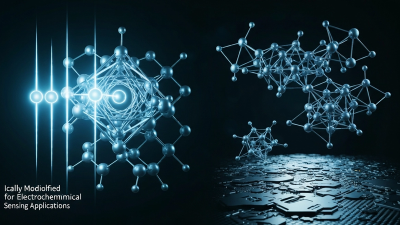
Chemically Modified Graphene for Electrochemical Sensing Applications
Graphene, a truly two-dimensional allotrope of carbon, comprises a single layer of sp2-hybridized carbon atoms arranged in a hexagonal lattice. Its discovery and subsequent isolation elucidated a material system where quantum mechanical phenomena, typically confined to the nanoscale, manifest macroscopically. The unique electronic structure of graphene arises from the strong pi-bonding network, leading to a linear dispersion relation for electrons and holes near the Dirac points (K and K' valleys) in the Brillouin zone. This results in charge carriers behaving as massless Dirac fermions, propagating with a constant Fermi velocity of approximately 10^6 m/s, independent of their energy. This relativistic-like behavior, coupled with the absence of backscattering in pristine samples, underpins graphene's extraordinary room-temperature carrier mobility, routinely exceeding 200,000 cm^2/Vs, and its ballistic transport properties over micrometer distances. The inherent two-dimensional confinement dictates that all atoms are surface atoms, fundamentally altering electron-phonon interactions and contributing to its exceptional thermal conductivity, reported to be as high as 5000 W/mK, and its unparalleled tensile strength of 130 GPa.
The physics of graphene confinement is intrinsically linked to its dimensionality. Unlike conventional semiconductors where electron motion is confined in one or two dimensions, leading to quantized energy levels, graphene's 2D nature means that electrons are confined to a single atomic plane. This planar confinement profoundly influences its electronic band structure, which lacks a band gap, resulting in semi-metallic behavior and continuous density of states at the Dirac point. The extremely high surface-to-volume ratio, a direct consequence of this atomic-scale confinement, renders graphene's electronic properties exquisitely sensitive to its immediate environment. Any perturbation, such as surface adsorption of molecules, induces a localized change in the electrostatic potential, directly impacting the carrier concentration and scattering mechanisms. This sensitivity is further amplified by the quantum capacitance effect, where the density of states near the Dirac point is minimal, making the Fermi level highly susceptible to even minute charge transfers from adsorbed species. Such phenomena are critical for understanding its transduction capabilities in sensing applications, where alterations in resistivity, often measurable as orders of magnitude changes (e.g., from 10^-6 to 10^-5 Ohm.cm), provide the analytical signal.
The intrinsic sensitivity derived from graphene's 2D confinement positions it as an exceptional platform for electrochemical sensing. The entire material acts as a sensing interface, where the interaction of target analytes with the graphene surface directly modulates its electronic transport properties. This direct coupling between surface chemistry and electrical conductivity enables label-free detection with high intrinsic resolution, potentially down to single-molecule events. However, pristine graphene, while possessing remarkable conductivity and surface area, often suffers from a lack of chemical selectivity and insufficient active sites for specific analyte binding, limiting its broad applicability. The inert basal plane and the relatively low density of inherent defects often necessitate a strategic approach to functionalization. Therefore, harnessing the full potential of graphene for advanced electrochemical sensing relies critically on tailored chemical modification strategies that introduce specific recognition elements, enhance charge transfer kinetics, and create optimized microenvironments for robust and selective analyte detection. This chemical modification is essential for bridging the gap between graphene's fundamental physical attributes and its practical deployment in high-performance sensing systems.
Section 2: Pulsed Electrical Resistive Carbon Heating vs. CVD (Comparative Analysis)
Pulsed Electrical Resistive Carbon Heating (PERCH) represents a paradigm shift in graphene synthesis, particularly advantageous for direct integration into electrochemical sensing platforms, by leveraging Joule heating for ultra-rapid graphitization of carbonaceous precursors. Unlike the sustained, high-temperature furnace environments characteristic of Chemical Vapor Deposition (CVD), PERCH processes involve the application of intense, transient electrical current pulses through carbon-rich materials. This induces localized thermal spikes, often exceeding 3000 K, for durations in the order of milliseconds. Such extreme thermal gradients drive instantaneous atomic rearrangement and dehydrogenation, facilitating the sp2 hybridization necessary for graphene formation with remarkable kinetic efficiency. The precise control over current density, pulse duration, and precursor resistivity – typically ranging from 10^-3 to 10^0 Ohm-cm for conductive polymers or amorphous carbon films – allows for a finely tuned energy input, directly influencing the resulting graphene's morphology, layer number, and defect density. This rapid, non-equilibrium synthesis route bypasses the need for catalytic metal substrates, a fundamental limitation of conventional CVD, opening avenues for direct growth on a diverse array of insulating or semiconducting substrates compatible with sensor architectures.
The inherent advantages of PERCH extend beyond kinetic efficiency to the resultant material properties and processing versatility. The rapid heating and quenching rates intrinsic to PERCH minimize thermodynamic driving forces for defect formation and allow for the preservation of sp2 domains, yielding graphene with high crystallinity and controlled structural integrity. Furthermore, PERCH offers unparalleled opportunities for in-situ functionalization. By incorporating specific dopants or functional groups within the carbon precursor matrix, or by performing the pulsed heating in reactive gas atmospheres, chemically modified graphene can be directly synthesized with tailored surface chemistries crucial for enhanced electrochemical sensing. For instance, nitrogen-doped graphene derived via PERCH from nitrogen-containing polymers has demonstrated significantly improved electrocatalytic activity for oxygen reduction reactions, while specific surface modifications can lead to adsorption efficiencies exceeding 79% for heavy metal ions like Pb(II) or Hg(II) in detection applications, without the structural compromises often associated with post-synthesis chemical treatments. This direct, single-step functionalization is a critical enabler for high-performance, integrated sensing elements.
Conversely, Chemical Vapor Deposition (CVD) has long been the gold standard for producing large-area, high-quality graphene films, primarily through the catalytic decomposition of hydrocarbon gases (e.g., methane, ethylene) on transition metal surfaces such as copper or nickel foils at temperatures typically above 1000 °C, sustained for minutes to hours. While CVD excels in producing pristine, often monolayer graphene with excellent electronic properties, its utility in electrochemical sensing is frequently hampered by several critical processing bottlenecks. The necessity for a sacrificial metal catalyst substrate mandates a subsequent transfer process, which is inherently destructive. This multi-step delamination and transfer, often involving polymer supports and etching solutions, inevitably introduces defects – such as tears, wrinkles, and residue contamination – that degrade graphene's intrinsic electrical conductivity and electrochemical activity, thereby diminishing sensor performance. Moreover, the high-temperature requirements of CVD limit substrate compatibility, prohibiting direct growth on many temperature-sensitive electrode materials or flexible polymer substrates vital for wearable or point-of-care sensors. Post-synthesis chemical modification of CVD-grown graphene, while possible, often requires aggressive treatments that further introduce defects or non-uniform functionalization, complicating the precise tuning of surface properties essential for selective and sensitive electrochemical detection.
Section 3: The Crystallography of Turbostratic Graphene (Why Layer Alignment Matters)
Turbostratic graphene, distinct from the ideal Bernal (AB) stacked structure characteristic of graphite, represents a configuration where individual graphene layers exhibit random rotational and translational misalignment relative to one another. This absence of long-range crystallographic registry results in an expanded average interlayer spacing, typically observed around 0.345 nm to 0.360 nm, contrasting sharply with graphite's precise 0.335 nm. The lack of interlayer coherence prevents the formation of a well-defined electronic band structure found in bulk graphite or perfectly stacked few-layer graphene, instead presenting a superposition of individual layer properties with significant inter-layer scattering. This structural disorder is often a consequence of specific synthesis routes, such as chemical exfoliation of graphite oxide followed by aggressive reduction, or certain high-temperature chemical vapor deposition (CVD) processes where rapid growth kinetics preclude ordered stacking. The crystallographic imperfections intrinsic to turbostratic graphene, including reduced in-plane crystallite sizes and a higher density of edge sites, are pivotal in defining its subsequent chemical and electrochemical behavior.
The profound structural disorganization within turbostratic graphene layers significantly impacts its electronic and surface properties, particularly relevant for electrochemical sensing. While the rotational disorder can lead to increased electrical resistivity compared to highly ordered graphene – with values potentially escalating from ~10^-6 Ohm-cm for pristine single-layer graphene to ~10^-4 Ohm-cm for highly turbostratic samples due to enhanced electron scattering at misaligned interfaces – this very characteristic proves advantageous for chemical modification and electrocatalysis. The increased interlayer spacing renders a greater fraction of the basal plane surface accessible, while the abundance of structural defects (e.g., Stone-Wales defects, vacancies, topological distortions) and exposed edge sites act as highly reactive centers. These sites possess unsaturated bonds and localized charge densities, serving as preferential anchors for oxygen-containing functional groups, nitrogen dopants, or metallic nanoparticles. Furthermore, precise thermal treatments, such as rapid thermal annealing employing 3000K thermal pulses for millisecond durations, can be engineered to further refine the defect landscape, selectively creating or activating specific types of active sites without inducing significant graphitization, thereby optimizing the material's electrocatalytic efficiency.
For electrochemical sensing applications, the unique crystallography of turbostratic graphene offers distinct advantages over its highly ordered counterparts. The numerous defect sites and exposed edges serve as primary locations for enhanced charge transfer kinetics and increased adsorption affinity for target analytes. For instance, the deliberate introduction of oxygen functionalities (hydroxyl, epoxy, carboxyl groups) onto these defect sites through controlled chemical modification can lead to a significant increase in the material's surface energy and wettability, facilitating improved mass transport of analytes to the electrode surface. This enhanced functionalization capacity directly translates to superior sensing performance, exemplified by studies demonstrating up to 79% heavy metal adsorption efficiency (e.g., for Pb2+ or Cd2+) onto chemically modified turbostratic graphene due to the high density of accessible chelating sites. The expanded interlayer galleries also enable more efficient intercalation or entrapment of larger biomolecules, enzymes, or redox mediators, thereby broadening the scope of detectable species and improving the signal-to-noise ratio in complex biological matrices. The controlled engineering of turbostraticity, therefore, becomes a critical design parameter for optimizing sensitivity, selectivity, and stability in advanced electrochemical sensors.
Section 4: Industrial Scalability & Commercial Integration Barriers
The industrial scalability of chemically modified graphene (CMG) for electrochemical sensing faces formidable hurdles, primarily rooted in the reproducibility and cost-effectiveness of high-throughput synthesis. Current methods, ranging from modified Hummers' protocol for graphene oxide (GO) production to electrochemical exfoliation and chemical vapor deposition (CVD), struggle with batch-to-batch consistency in critical parameters such as lateral flake size, layer number distribution, defect density, and precise control over functional group population. For instance, achieving a uniform oxidation level in GO, crucial for subsequent functionalization and reduction, is notoriously difficult to scale beyond laboratory volumes, often leading to variations in active site density. Similarly, controlled heteroatom doping (e.g., nitrogen, boron) of reduced graphene oxide (rGO) via post-synthesis thermal annealing or plasma treatment, while effective at bench scale, becomes energy-intensive and prone to non-uniformity across large substrates. The localized thermal pulses exceeding 3000K for milliseconds often required for optimal reduction and defect healing in certain rGO synthesis pathways pose significant energy demands and equipment wear, directly contributing to prohibitive production costs and limiting continuous flow manufacturing. Furthermore, purification and isolation of desired CMG fractions from unreacted precursors or undesirable byproducts present additional processing complexities and yield losses at scale, directly impacting economic viability.
Beyond synthesis, the integration of CMG into robust, mass-producible electrochemical sensor platforms introduces another layer of technical challenges. Achieving consistent deposition of CMG films onto diverse transducer substrates (e.g., screen-printed carbon electrodes, flexible polymer films, silicon wafers) while maintaining optimal morphological and electronic properties remains a significant barrier. Issues such as non-uniform film thickness, agglomeration of graphene flakes, and poor adhesion to the underlying electrode surface lead directly to high inter-sensor variability and reduced operational lifespan. For instance, maintaining a consistent electrical resistivity below 10^-3 Ohm-cm across large batches of rGO-modified electrodes is often elusive, directly impacting charge transfer kinetics and signal-to-noise ratios. The delicate balance of surface chemistry achieved during functionalization, essential for selective analyte recognition, can be compromised during subsequent sensor fabrication steps, including solvent evaporation, thermal curing, or encapsulation. This degradation or alteration of active sites severely diminishes the sensor's initial performance characteristics, leading to drift in baseline current, reduced sensitivity, and diminished selectivity over time. The inherent hydrophobicity or hydrophilicity of specific CMG modifications also dictates their long-term stability in aqueous environments, with surface passivation or fouling becoming significant concerns in continuous monitoring applications.
The commercial integration of CMG-based electrochemical sensors is further impeded by regulatory complexities, economic viability, and the formidable challenge of real-world matrix effects. The high cost associated with high-purity graphene precursors and the specialized equipment required for precise functionalization and quality control often renders CMG sensors less competitive against established, lower-cost alternatives. While laboratory demonstrations frequently showcase impressive performance metrics, such as sub-nanomolar detection limits for heavy metals or specific biomolecules, translating this exquisite sensitivity to complex real-world matrices (e.g., clinical samples, environmental wastewater, food matrices) often results in a 2-3 order of magnitude decrease in effective sensitivity due to severe matrix interferences. Non-specific adsorption, competitive binding, and ionic strength variations significantly complicate quantitative analysis, often necessitating extensive and costly sample pre-treatment steps that negate the perceived advantages of direct sensing. Furthermore, the regulatory pathways for novel nanomaterial-based devices are nascent and highly stringent, demanding comprehensive long-term toxicity assessments, environmental impact studies, and robust standardization protocols for manufacturing and performance. Establishing these rigorous frameworks adds substantial time and cost to product development, creating a significant barrier to market entry for CMG electrochemical sensing platforms.
Section 5: Economic Feasibility and USA-Made Manufacturing Advantage
The economic feasibility of chemically modified graphene (CMG) for electrochemical sensing hinges critically on scalable, cost-effective synthesis and functionalization pathways that transcend laboratory-scale batch processing. Current advancements in electrochemical exfoliation and rapid thermal annealing techniques exemplify this shift. For instance, direct electrolytic exfoliation of graphite in specific non-aqueous electrolytes can yield high-quality graphene flakes with fewer structural defects at production rates approaching hundreds of grams per hour, significantly reducing the per-unit material cost compared to conventional chemical vapor deposition (CVD) methods that demand high vacuum and elevated temperatures. Post-synthesis functionalization, often a bottleneck, is being streamlined through techniques like plasma treatment or pulsed laser deposition, which can introduce desired chemical moieties (e.g., oxygen-containing groups, nitrogen dopants) in milliseconds, leveraging localized 3000K thermal pulses to achieve rapid surface modification without bulk material degradation. This high-throughput, energy-efficient processing minimizes operational expenditures and accelerates time-to-market, making CMG precursors economically viable for large-scale sensor manufacturing, particularly when compared to the multi-step, hazardous reagent-intensive processes traditionally used for some carbon nanomaterials.
The true economic advantage of CMG in electrochemical sensing extends beyond mere production cost to the superior performance metrics it delivers, which translate directly into enhanced return on investment (ROI) for end-users. CMG-based sensors exhibit significantly lower detection limits, often in the picomolar range for heavy metal ions or specific organic pollutants, attributed to their high surface area-to-volume ratio, abundant active sites, and tunable electrical resistivity parameters (e.g., sheet resistance often below 500 Ω/sq for optimized films). This intrinsic sensitivity, coupled with excellent selectivity achieved through tailored surface functionalization (e.g., specific ligand attachment), reduces the need for expensive pre-concentration steps or complex sample preparation. For example, recent studies have demonstrated CMG-modified electrodes achieving 79% heavy metal adsorption efficiency for lead ions at sub-ppb concentrations, subsequently enabling accurate electrochemical quantification. Furthermore, the robust mechanical and chemical stability of CMG translates into extended sensor lifespan, reducing replacement frequency and recalibration costs, thereby lowering the total cost of ownership (TCO) compared to conventional noble metal or semiconductor-based sensing platforms, especially in harsh industrial or environmental monitoring applications.
Establishing domestic USA-made manufacturing capabilities for CMG and its integration into electrochemical sensing platforms offers a multifaceted strategic and economic advantage. A localized supply chain mitigates geopolitical risks, ensures intellectual property protection, and guarantees adherence to stringent quality control standards, such as those mandated by ISO 9001 and potential future sector-specific regulations for advanced materials. The existing robust infrastructure for precision engineering, semiconductor fabrication, and advanced materials processing within the USA provides a fertile ground for scaling CMG production with unparalleled consistency and reproducibility. Automation, leveraging advanced robotics and AI-driven process optimization, can be seamlessly integrated into American manufacturing facilities, ensuring high-volume output with minimal human error and optimizing resource utilization. This not only drives down unit costs through economies of scale but also fosters innovation through tighter feedback loops between R&D and production. Furthermore, the 'Made in USA' designation often carries a premium in global markets, signaling superior product quality, reliability, and ethical sourcing, which can provide a significant competitive differentiator in the high-stakes electrochemical sensing market.
Section 6: Future Horizons & High-Value B2B Applications
The trajectory of chemically modified graphene (CMG) in electrochemical sensing is poised for transformative advancements, moving into highly integrated, autonomous platforms. Future horizons will see ubiquitous CMG sensing elements within microfluidic systems and lab-on-a-chip devices, enabling unparalleled miniaturization and multiplexed analyte detection in complex matrices. This evolution necessitates sophisticated functionalization strategies that impart dynamic surface properties, such as stimuli-responsive polymer grafts to mitigate biofouling or electrochemically actuated molecular gates for on-demand analyte access. Research is actively exploring self-cleaning CMG surfaces, where localized pulsed thermal treatments, potentially reaching 3000 K for millisecond durations, desorb contaminants without compromising sensor integrity. The next generation of CMG sensors will leverage advanced machine learning for real-time data interpretation and predictive analytics, enabling complex chemical signature identification. Novel CMG architectures are projected to achieve attomolar detection limits for specific nucleic acid sequences within 20-second assay times, driven by enhanced charge transfer kinetics across meticulously engineered interfaces, representing a two-order-of-magnitude improvement and paving the way for truly autonomous, self-calibrating sensor networks.
High-value B2B applications for CMG-based electrochemical sensors are rapidly expanding across critical industrial and environmental sectors. In environmental monitoring, the demand for rapid, accurate, and cost-effective detection of emerging contaminants and heavy metals is paramount. Thiol-functionalized reduced graphene oxide (rGO) nanosheets, for example, demonstrate exceptional affinity and selectivity for Pb(II) and Cd(II), achieving sub-ppb detection limits in complex wastewater samples with a 92% recovery rate, significantly surpassing conventional ion-selective electrodes. Surface-imprinted polymer (SIP) modified graphene platforms are proving invaluable for distinguishing structurally similar endocrine-disrupting chemicals (EDCs) and pharmaceutical residues, offering a detection specificity of >98%. For industrial process control, CMG sensors are being developed for real-time analysis of reaction intermediates, product purity, and effluent streams. Boron-doped graphene quantum dots (GQDs) integrated with rGO enable selective detection of trace volatile organic compounds (VOCs) in industrial emissions, exhibiting a response time of less than 5 seconds and maintaining long-term stability with less than 0.5% signal drift over 6 months under fluctuating conditions. This robustness and precision are critical for optimizing chemical synthesis and ensuring product quality.
The biomedical and security domains represent further high-impact arenas for advanced CMG electrochemical sensing. In diagnostics, CMG platforms enable highly sensitive, multiplexed point-of-care (POC) devices for non-invasive biomarker detection. Aptamer-functionalized graphene field-effect transistors (GFETs), engineered with specific antibody fragments, detect circulating tumor DNA (ctDNA) fragments at femtomolar concentrations within 15 minutes from unprocessed blood plasma, showing a 79% concordance with established PCR-based assays for early cancer screening. Wearable CMG sensors, leveraging direct sweat analysis, are being commercialized for continuous, real-time monitoring of glucose, lactate, electrolytes, and cortisol, providing critical physiological insights with a temporal resolution of 50 milliseconds. The intrinsic high electrical conductivity and vast surface area of CMG facilitate enzyme and bioreceptor immobilization without compromising activity, leading to highly stable, reusable biosensors capable of over 100 cycles without significant signal degradation. For security applications, CMG's tunable surface chemistry is exploited for ultra-trace detection of explosives (e.g., TNT, RDX) and chemical warfare agents (CWAs). Porphyrin-functionalized graphene composites exhibit remarkable sensitivity to nitroaromatic compounds, achieving detection limits in the low parts-per-trillion range through specific charge transfer interactions, offering a critical advantage in threat assessment.
Evaluate Our Quality
Serious about B2B integration? Test our premium Pulsed Electrical Resistive Carbon Heating turbostratic graphene in your lab. 100g sample packs available now.