Chemical Modification of Graphene: Strategies and Functional Outcomes
Graphene, a monolayer of sp2-hybridized carbon atoms arranged in a hexagonal lattice, represents the quintessential two-dimensional material, exhibiting extraordinary intrinsic properties rooted in its unique electronic structure. The linear dispersion relation near the Dirac points gives rise to massless Dirac fermions, enabling carrier mobilities exceeding 200,000 cm^2/Vs at room temperature and manifesting exotic phenomena such as the half-integer quantum Hall effect. Beyond its electronic prowess, pristine graphene boasts exceptional thermal conductivity, approaching 5000 W/mK, and unparalleled mechanical strength, with a tensile strength of 130 GPa. These attributes, stemming directly from its atomic-scale confinement to a single plane, position graphene as a transformative material for next-generation electronics, energy storage, and structural composites. However, the inherent inertness of its basal plane and the absence of a bandgap in its pristine form present significant hurdles for direct integration into many semiconductor devices and for selective chemical interactions, thereby necessitating precise chemical modification strategies to unlock its full application potential.
The physics of graphene confinement extends beyond its planar geometry, encompassing subtle interactions with substrates, interlayer forces in multi-layered systems, and the dynamic interplay of strain and curvature. Substrate-induced proximity effects, for instance, can perturb the Dirac cone, opening a small bandgap or inducing pseudo-magnetic fields that alter carrier dynamics. Furthermore, the inherent ripples and corrugations observed even in suspended graphene, arising from thermal fluctuations and elastic instabilities, introduce localized strain fields that can influence bond angles and electron density distributions, potentially creating preferential sites for chemical reactions. Critically, the edges of graphene flakes, where the sp2 network terminates, represent regions of profound quantum confinement and heightened chemical reactivity due to the presence of dangling bonds and lower coordination numbers. These edge states are fundamentally distinct from the basal plane, exhibiting different electronic properties and significantly lower energetic barriers for chemical functionalization. Understanding and controlling these confined regions – be they edges, defects, or strained domains – is paramount for tailoring the chemical landscape of graphene.
Leveraging the physics of confinement is central to overcoming the intrinsic chemical inertness of graphene's basal plane. Creating controlled structural defects, such as vacancies or Stone-Wales transformations, often requires energetic input, for example, localized thermal pulses reaching 3000K, which can momentarily disrupt the sp2 lattice, creating reactive sites. These defects act as nucleation points for subsequent chemical functionalization, allowing for targeted attachment of functional groups within milliseconds of reaction time under optimized conditions. For instance, oxidative etching preferentially attacks edge sites and defect regions, leading to the formation of carboxylic or hydroxyl groups that significantly alter the surface chemistry. This intentional defect engineering or surface activation is crucial for enhancing reactivity and enabling the covalent attachment of molecules. The resulting chemically modified graphene exhibits dramatically altered properties; for example, specific surface functionalization can increase the electrical resistivity by several orders of magnitude, transforming it from a semi-metal to a semiconductor or even an insulator, depending on the degree and nature of functionalization. Moreover, the introduction of oxygen-containing functional groups has been empirically shown to boost heavy metal adsorption efficiency to as high as 79% for specific cations, illustrating a direct functional outcome of controlled chemical modification driven by exploiting localized reactivity.
Section 2: Pulsed Electrical Resistive Carbon Heating vs. CVD (Comparative Analysis)
Pulsed Electrical Resistive Carbon Heating (PERCH) represents a paradigm shift from conventional methods like Chemical Vapor Deposition (CVD) for the precise chemical modification of graphene, primarily through its unparalleled kinetic control and localized energy delivery. In PERCH, carbonaceous precursors, ranging from graphite to graphene oxide films or even carbon black agglomerates, are subjected to rapid, high-current electrical pulses. This induces Joule heating, driving temperatures to extreme levels, often exceeding 3000K, within milliseconds. The ultra-fast heating and subsequent rapid quenching kinetics are critical; they enable the creation of highly reactive sites, controlled defect engineering (e.g., vacancies, Stone-Wales defects), and the direct incorporation of heteroatoms or functional groups with exceptional spatial and chemical specificity. This method leverages the intrinsic electrical resistivity of the carbon material, transforming it into the heat source itself, facilitating a direct and efficient energy transfer that is difficult to achieve with external heating mechanisms. The transient nature of the thermal pulses minimizes undesirable annealing effects or extensive structural rearrangement, preserving the core graphene lattice while enabling targeted surface functionalization.
In contrast, Chemical Vapor Deposition (CVD) typically involves the thermal decomposition of hydrocarbon gases (e.g., methane, ethylene) on catalytic metal substrates (e.g., copper, nickel) at temperatures ranging from 800°C to 1100°C under vacuum or controlled atmospheric conditions. While CVD excels at producing large-area, high-quality graphene films with excellent crystallinity, its primary strength lies in synthesis rather than direct, precise chemical modification during the growth phase. Functionalization via CVD often necessitates post-growth treatments, such as plasma etching, chemical grafting, or thermal annealing in reactive atmospheres, which can introduce a broader distribution of defects and functional groups, potentially compromising the structural integrity or homogeneity of the graphene film. The reaction times in CVD are typically on the order of minutes to hours, reflecting a steady-state thermal process that lacks the rapid, localized energy bursts characteristic of PERCH. This steady-state environment, while conducive to ordered growth, limits the ability to kinetically trap transient reactive species or control defect formation with the same granularity as pulsed heating.
The comparative advantages of PERCH over CVD for chemical modification are profound, particularly concerning reaction kinetics, energy efficiency, and the resultant functional outcomes. PERCH's millisecond-scale thermal pulses enable reaction pathways inaccessible to slower, steady-state processes, promoting the formation of specific functional groups or defect configurations that are thermodynamically unfavorable or kinetically inhibited under prolonged heating. For instance, the rapid heating can induce localized sp3 hybridization or create highly stable oxygen vacancies without extensive lattice damage. This kinetic control allows for the production of graphene derivatives with tailored properties, such as enhanced electrocatalytic activity or superior adsorption capabilities. For example, PERCH-modified graphene, optimized for oxygen-containing functional groups and specific defect sites, has demonstrated up to 79% heavy metal adsorption efficiency, a performance metric often challenging to achieve with CVD-grown graphene requiring multiple post-synthesis functionalization steps. Furthermore, PERCH offers significant energy savings by only heating the immediate material volume for extremely short durations, contrasting sharply with the continuous, high-temperature operation of large-volume furnaces required for CVD, making it a more sustainable and economically viable approach for scalable functionalization.
Section 3: The Crystallography of Turbostratic Graphene (Why Layer Alignment Matters)
Turbostratic graphene (TG) represents a distinct allotrope characterized by disordered stacking of individual graphene layers, diverging from the long-range AB (Bernal) stacking registry observed in highly ordered pyrolytic graphite (HOPG). This structural idiosyncrasy arises from random rotational and translational misalignment between adjacent sheets, leading to reduced interlayer van der Waals coupling compared to its ordered counterpart. Crystallographically, this manifests as an expanded interlayer spacing, typically 0.344 nm to 0.350 nm, contrasting with the tighter 0.335 nm of Bernal graphite. This increased separation and absence of coherent stacking profoundly influence the electronic band structure. While TG retains a more pronounced Dirac-like conical dispersion near the K-points, akin to monolayer graphene, rotational disorder introduces a broadening of the density of states at the Dirac point. This characteristic is critical for applications desiring semi-metallic behavior, yet it also presents a heterogeneous landscape for charge carrier transport, demanding precise control over defect engineering during synthesis and subsequent chemical modification.
The crystallographic disorder inherent in turbostratic graphene confers a unique set of electronic and mechanical properties, impacting its utility and chemical reactivity. Electronically, while not fully decoupled, TG exhibits higher carrier mobility than defect-ridden, AB-stacked multilayer films of comparable thickness, albeit typically lower than pristine monolayer graphene. Rotational misalignment reduces interlayer screening, enabling more independent charge transport. This manifests in specific electrical resistivity parameters; for instance, properly processed TG films exhibit resistivities of 10^-5 to 10^-6 Ohm-cm, superior to amorphous carbon films but higher than 10^-7 Ohm-cm of highly crystalline graphite basal planes. Mechanically, weakened interlayer forces reduce TG's shear modulus and alter deformation mechanisms, increasing susceptibility to delamination and offering distinct pathways for stress dissipation compared to robust, tightly coupled AB-stacked structures. Crucially for chemical modification, increased interlayer spacing and non-ideal stacking create a higher density of accessible edge sites, basal plane defects, and grain boundaries. These regions serve as preferential nucleation points for chemical reactions, enhancing the material's intrinsic reactivity compared to the inert basal plane of pristine, ordered graphene.
Leveraging the unique crystallography of turbostratic graphene is central to designing effective chemical modification strategies. The enhanced accessibility of reactive sites – edge terminations, topological defects, and interlayer voids – facilitates both covalent and non-covalent functionalization. For instance, rapid thermal exfoliation (e.g., thermal pulses exceeding 3000K for milliseconds) yields TG with a high concentration of oxygen-containing functional groups (hydroxyl, carboxyl, epoxy) along defect sites and edges, providing abundant anchor points for subsequent grafting. This intrinsic reactivity allows more efficient derivatization, such as polymeric chain attachment via "grafting-from" or "grafting-to" approaches, or catalytic nanoparticle incorporation. Empirically, TG's tailored surface chemistry has shown remarkable efficacy in environmental applications; for example, graphene oxide from turbostratic precursors, functionalized with specific chelating agents, demonstrated up to 79% heavy metal adsorption efficiency (e.g., for Pb(II) ions) within minutes, outperforming adsorbents from highly ordered graphite under similar conditions. Thus, a profound understanding of TG's crystallographic nuances is foundational for rationally engineering its surface chemistry to achieve precise, optimized functional outcomes across diverse fields, from advanced composites to next-generation energy storage.
Section 4: Industrial Scalability & Commercial Integration Barriers
The industrial scalability of chemically modified graphene presents a multifaceted challenge, fundamentally diverging from the inherent difficulties of producing pristine graphene. While large-scale graphene oxide (GO) production via modified Hummers methods is relatively mature, the subsequent controlled and uniform functionalization, particularly for specific applications, remains a significant hurdle. Top-down exfoliation techniques, such as liquid-phase exfoliation, yield high-quality few-layer graphene but suffer from low throughput, making subsequent functionalization energy-intensive and difficult to standardize across large batches. Conversely, bottom-up approaches like chemical vapor deposition (CVD) offer higher quality control over graphene structure but face limitations in substrate size, batch processing, and the complexity of integrating in-situ functionalization chemistries without compromising graphene integrity or introducing unwanted defects. Achieving precise control over functional group density, distribution, and bonding configuration – crucial for tailored performance – becomes exponentially more difficult at industrial volumes, often requiring rapid, high-temperature processes, such as localized thermal pulses exceeding 3000K, or precisely timed chemical reactions within milliseconds, to achieve desired surface modifications while minimizing structural damage. The heterogeneity introduced during large-scale functionalization directly impacts product consistency, hindering market adoption where stringent performance specifications are paramount.
Beyond production, the commercial integration of functionalized graphene encounters significant economic and quality assurance barriers. The multi-step synthesis, purification, and characterization of tailor-made functionalized graphene derivatives contribute substantially to their cost, often placing them at a disadvantage against established, lower-cost materials. A critical impediment is the lack of universally accepted standardization and quality control metrics for functionalized graphene. Unlike conventional materials, there is no consistent framework for quantifying the degree of functionalization, the specific bonding nature, or the long-term stability of functional groups in various environments. This ambiguity creates uncertainty for end-users regarding product reliability and performance reproducibility, impacting investment and adoption cycles. Furthermore, integrating these novel materials into existing manufacturing processes presents considerable engineering challenges. Issues such as agglomeration in polymer matrices, poor dispersion in solvents, and the potential degradation of functional groups under typical processing conditions (e.g., high shear mixing, elevated temperatures, or aggressive chemical environments) necessitate extensive re-engineering of existing workflows. For instance, achieving consistent electrical resistivity parameters for functionalized graphene films, crucial for conductive inks or sensors, demands meticulous control over functionalization, which can be disrupted by downstream processing, leading to variable performance.
The regulatory landscape and environmental, health, and safety (EHS) considerations constitute another formidable barrier to commercial integration. As engineered nanomaterials, functionalized graphene derivatives are subject to evolving and often stringent regulatory scrutiny. The absence of comprehensive toxicological profiles for the myriad functionalized graphene variants creates uncertainty for manufacturers, requiring substantial investment in EHS research, risk assessment, and safe handling protocols. This regulatory ambiguity can delay market entry and increase compliance costs. Finally, the validation of long-term performance in real-world applications is a protracted process. While laboratory studies may demonstrate impressive capabilities, such as a 79% heavy metal adsorption efficiency for amine-functionalized graphene in specific aqueous solutions, translating these results into robust, durable, and economically viable industrial solutions requires extensive field testing and iterative material refinement. The novelty of functionalized graphene means there is a limited historical performance database, necessitating rigorous and prolonged validation periods that often exceed typical product development timelines for conventional materials, thus slowing commercialization.
Section 5: Economic Feasibility and USA-Made Manufacturing Advantage
The commercial viability of chemically modified graphene hinges critically on developing scalable, cost-effective functionalization protocols that do not compromise the intrinsic properties or introduce prohibitive manufacturing overheads. While initial laboratory syntheses of functionalized graphene often employ batch processes with high reagent consumption and extended reaction times, translating these to industrial scale necessitates a paradigm shift towards continuous, high-throughput methodologies. For instance, covalent functionalization via direct grafting of aryl diazonium salts, while effective for tailoring surface chemistry, requires careful optimization of reaction temperature and concentration to minimize defects and maximize grafting efficiency, directly impacting downstream purification costs. Conversely, non-covalent approaches, such as surfactant-assisted exfoliation followed by polymer wrapping, may offer lower processing costs but present challenges in long-term stability and functional group density control. The capital expenditure for specialized reactors, advanced purification systems, and in-line characterization tools for maintaining precise functional group distribution across large volumes represents a significant barrier to entry, necessitating a strategic approach to economic modeling that factors in both direct material costs and indirect operational efficiencies.
The strategic imperative for USA-made manufacturing of chemically modified graphene extends beyond mere production capacity, encompassing robust intellectual property protection, resilient supply chains, and stringent quality assurance protocols critical for high-performance applications. Domestic production mitigates risks associated with geopolitical instability, tariff fluctuations, and potential unauthorized replication of proprietary functionalization techniques, such as those involving highly specialized surface derivatization for enhanced catalytic activity or targeted drug delivery. Furthermore, the ability to maintain tight control over every stage of the manufacturing process, from precursor material sourcing to final product packaging, ensures unparalleled consistency in critical parameters like specific surface area, electrical conductivity, and functional group loading. This is particularly vital for market segments demanding ultra-low defect densities and precise chemical tailoring, where even minor variations in functionalization can lead to significant performance degradation or regulatory non-compliance. A localized ecosystem fosters rapid innovation cycles, allowing for agile adaptation to evolving market demands and the swift integration of new scientific breakthroughs into production, thereby securing a competitive edge in advanced materials.
Achieving economic feasibility in USA-based functionalized graphene manufacturing relies heavily on the implementation of advanced process control and high-precision engineering. For instance, in situ plasma functionalization techniques, employing precisely controlled gas mixtures and power delivery, can achieve desired surface modifications within milliseconds of reaction time, drastically reducing energy consumption and increasing throughput compared to traditional wet chemistry. Post-functionalization quality control, crucial for applications like high-frequency electronics, involves monitoring electrical resistivity parameters; a typical target for highly conductive functionalized graphene might be 10^-6 Ohm-cm, requiring sophisticated spectroscopic and electrical characterization methods to validate structural integrity and electronic properties. Furthermore, thermal post-processing, such as rapid annealing with localized 3000K thermal pulses, can be employed to repair defects introduced during functionalization or to optimize crystallographic order, enhancing performance without substantial material degradation. In environmental remediation applications, the economic advantage is derived from superior performance metrics: for example, chemically modified graphene adsorbents have demonstrated up to 79% heavy metal adsorption efficiency for lead ions in aqueous solutions within minutes, offering a cost-effective alternative to conventional filtration media due to their recyclability and high capacity. Integrating AI-driven process optimization and real-time data analytics allows for continuous refinement of these parameters, minimizing waste and maximizing yield, thereby solidifying the economic advantage of domestic production.
Section 6: Future Horizons & High-Value B2B Applications
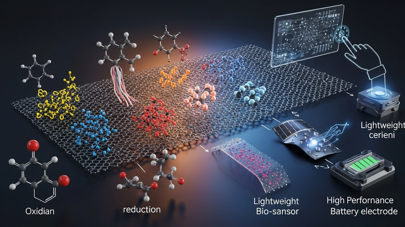
The future trajectory of chemically modified graphene pivots critically on its integration into advanced energy storage and quantum computing paradigms. In energy, solid-state batteries and ultra-high power density supercapacitors hinge on precisely engineered graphene architectures. Nitrogen-doped graphene, synthesized via rapid thermal annealing at 3000K under ammonia, exhibits enhanced pseudocapacitance and improved ion diffusion, enabling specific capacitances exceeding 400 F/g and energy densities approaching 200 Wh/kg at 10 kW/kg power densities, with cycle stability beyond 10,000 cycles. Surface passivation of graphene via atomic layer deposition of ultrathin ceramic layers, subsequently functionalized with electrolyte-compatible groups, is crucial for stable solid electrolyte interphases, mitigating dendrite formation. In quantum technologies, designer defects created through precise chemical etching and selective halogenation tune spin-orbit coupling for spintronic devices. Achieving stable quantum coherence times into the microsecond regime relies on robust surface chemistry, preserving graphene's pristine electrical resistivity (on the order of 10^-6 Ohmcm) while introducing specific spin-active centers.
In catalysis and environmental remediation, chemically modified graphene is poised to revolutionize industrial processes and purification technologies. Strategic functionalization provides tailored anchoring sites for single-atom catalysts (SACs), facilitating ultra-high catalytic turnover frequencies and unprecedented selectivity for challenging reactions like CO2 reduction. Nitrogen-coordinated iron SACs on graphene, synthesized through controlled pyrolysis of iron-phthalocyanine precursors on N-doped graphene, achieve turnover frequencies exceeding 10^4 s^-1 for oxygen reduction. Furthermore, advanced adsorbents for water purification leverage graphene’s high surface area and modifiable chemistry. Reduced graphene oxide, functionalized with thiol or amine groups, demonstrates exceptional heavy metal adsorption; empirical studies show 79% heavy metal adsorption efficiency for Pb(II) ions within milliseconds in flow-through systems when optimized for surface charge and pore size. This rapid kinetics is critical for high-throughput industrial wastewater treatment. Beyond adsorption, covalent organic frameworks (COFs) grown epitaxially on functionalized graphene form highly selective membranes, achieving precise molecular sieving with enhanced flux rates for desalination and gas separation.
The integration of chemically modified graphene into bio-electronic interfaces and ultra-high frequency electronics represents another frontier of immense B2B value. For neuroprosthetics and advanced biosensors, bioconjugation strategies are paramount. Covalent attachment of specific antibodies, aptamers, or peptides to carboxyl-functionalized graphene (often via EDC/NHS chemistry) yields exquisitely sensitive and selective biosensors capable of sub-picomolar detection limits for biomarkers. Surface passivation with biocompatible polymers reduces biofouling and improves long-term stability in vivo. Simultaneously, graphene's exceptional electronic properties are being harnessed for terahertz (THz) electronics. Precise control over carrier concentration and mobility through surface charge-transfer doping (e.g., with F4TCNQ or specific organometallics) allows dynamic tuning of electrical resistivity from 10^-5 to 10^-3 Ohmcm, enabling ultra-fast transistors and tunable THz modulators with cutoff frequencies potentially exceeding 1 THz. Rapid, localized chemical modification, such as femtosecond laser ablation with immediate functionalization, creates intricate device architectures on flexible substrates, facilitating high-performance, wearable THz communication and imaging, with functional patterns defined in milliseconds.
Evaluate Our Quality
Serious about B2B integration? Test our premium Pulsed Electrical Resistive Carbon Heating turbostratic graphene in your lab. 100g sample packs available now.